Article

A Reconfigurable SRAM CRP PUF with High Reliability and Randomness

1
School of Electrical Engineering, Chungbuk National University, Cheongju 28644, Republic of Korea
2
Department of Electronic Engineering, Seoul National University of Science and Technology, Seoul 01811, Republic of Korea
*
Author to whom correspondence should be addressed.
Electronics 2024, 13(2), 309; https://doi.org/10.3390/electronics13020309
Submission received: 24 November 2023 / Revised: 22 December 2023 / Accepted: 8 January 2024 / Published: 10 January 2024
(This article belongs to the Section Circuit and Signal Processing)

Abstract

:
This paper presents a novel reconfigurable SRAM CRP PUF that can achieve high reliability and randomness. In conventional reconfigurable SRAM CRP PUFs, imprecise timing control can produce a biased response output, which is typically attributed to mismatches in the connection of input control signals to the two inverter arrays in the layout floorplan. We propose a timing control scheme along with the addition of an adjunct NMOS transistor to address this issue. This eliminates the connection mismatches for the challenge and word-line inputs to the two inverter arrays. Furthermore, we employ symmetric layout techniques to achieve the randomness of response output. The symmetric arrangement of the two inverter arrays maximizes the inherent random output characteristics derived from process variation. The pre-charge input signal is symmetrically connected to each array to prevent delay mismatches. A 16 × 9-bit reconfigurable PUF array is fabricated by using a 180 nm CMOS process, with a PUF cell area of 1.2 × 10 4 F 2 /bit. The experimental results demonstrate an inter Hamming distance of 0.4949 across 40 chips and an intra Hamming distance of 0.0167 for a single chip in 5000 trials. The measured worst bit error rate (BER) is 4.86% at the nominal point (1.8 V, 25 °C). The proposed prototype exhibits good reliability and randomness, as well as a small silicon area when compared to the conventional SRAM CRP PUFs.

1. Introduction

The rapid development of the internet of things (IoT) has ushered in an era of unprecedented connectivity and innovation, with IoT devices permeating virtually every aspect of our lives, owing to their efficiency, convenience, and insight. However, this connectivity necessitates enhanced security to address potential vulnerabilities such as unauthorized access, data breaches, and cyberattacks [1]. Existing security measures face various drawbacks, including resource constraints on IoT devices, cryptographic complexity, and evolving adversarial tactics [2,3]. Alternative security paradigms suitable for the IoT’s unique attributes must be explored to address these challenges. Physically unclonable functions (PUFs) present considerable potential due to their uniqueness, lightweight nature, and minimal resource requirements [4]. PUFs leverage inherent variations in electronic devices during manufacturing, providing distinct and unpredictable outputs for each device. This makes them ideal for secure cryptographic key generation and robust authentication [5,6]. By harnessing physical variations’ inherent randomness and uniqueness, PUFs present a dependable and tamper-resistant solution, as they can safeguard sensitive information and ensure digital system integrity. Unlike conventional cryptographic methods that depend on key storage, PUFs do not require the storage of sensitive data, enhancing their resilience to attacks [7].
PUFs can be categorized into non-silicon and silicon-based types [8]. Non-silicon PUFs present various physical properties of materials, such as optical [9], polymer-based [10], magnetic [11], carbon-based [12], and photonic crystal [13], and so on. They exploit specific material properties to generate unique challenge-response pairs. Conversely, silicon-based PUFs depend on inherent variations from manufacturing processes and environmental factors in silicon semiconductor devices. Silicon PUFs present various advantages, particularly their seamless integration into existing semiconductor technology, making them ideal for resource-constrained IoT environments.
Silicon-based PUFs can be classified into two main categories based on their strength level corresponding to the number of Challenge–Response Pairs (CRPs): strong PUFs and weak PUFs. Weak PUFs produce a limited number of CRPs. These PUFs are ideally used in chip identification and cryptographic key generation [14]. Conversely, strong PUFs generate an extensive array of CRPs [15]. The availability of multiple CRPs enables the use of different challenges in multiple sessions without exhausting the pool of unique responses. Strong PUFs present excellent device identification and authentication protocols, ensuring a higher level of security against sophisticated attacks [16].
Extensive research has been conducted to develop strong PUF owing to their exceptional advantages [17,18,19,20,21]. For instance, a bistable ring (BR) comprising an even number of inverters is transformed into a strong BR PUF [17]. Ref. [18] presents a novel method for enhancing the CRP set of conventional ring oscillator-based PUFs. The reconfigurability presented in [19] exponentially increases the number of CRPs, presenting a strong Arbiter PUF (APUF) based on a typical 1T-1R RRAM array architecture. Furthermore, Ref. [20] presents a strong PUF generated from an existing weak switched-capacitor (SC)-based PUF. Ref. [21] presented a strong PUF using diode-clamped inverters operating in the subthreshold region. However, the large area requirement and power consumption of these devices considerably limit their implementation in IoT devices.
Ref. [22] presented a pioneering approach to a strong PUF design, featuring a reconfigurable SRAM-based architecture with multiple CRPs. This PUF presented high power efficiency and compact area, while maintaining good CRP density. These characteristics make it particularly suitable for the authentication of IoT devices. However, this design exhibits a correlation between the response outputs, even with different challenge inputs. This potential correlation is attributed to the inevitable mismatch in parasitic composition along the input signal paths to the two inverter arrays in the layout design. This mismatch results in the PUF cell becoming independent of the challenge input and producing a fixed response output. This paper proposes an operation timing control scheme to eliminate the mismatch of challenge and word-line inputs in order to solve this problem. The proposed timing scheme requires a modification of the structure by adding adjunct NMOS to eliminate the influence of the challenge input on the SRAM operation in generating a random response output. Subsequently, a symmetrical inverter array arrangement technique is used to maximize the effects of process variation. Simultaneously, the pre-charge input signal is also symmetrically connected to the two inverter arrays to minimize the delay mismatch.
The remainder of this paper is organized as follows. Section 2 describes the structure and operation of the conventional SRAM CRP PUF in [22], along with an analysis of the existing issues. Section 3 introduces the proposed SRAM CRP PUF, incorporating a symmetrical layout design technique, and presents the simulation results that demonstrate its effectiveness. Section 4 discusses the implementation of the SRAM CRP PUF system. Section 5 details the measurement results of our PUF using prototypes deployed on a 180 nm CMOS process, presenting a comparison with the existing state-of-the-art PUFs. Lastly, Section 6 concludes our work.

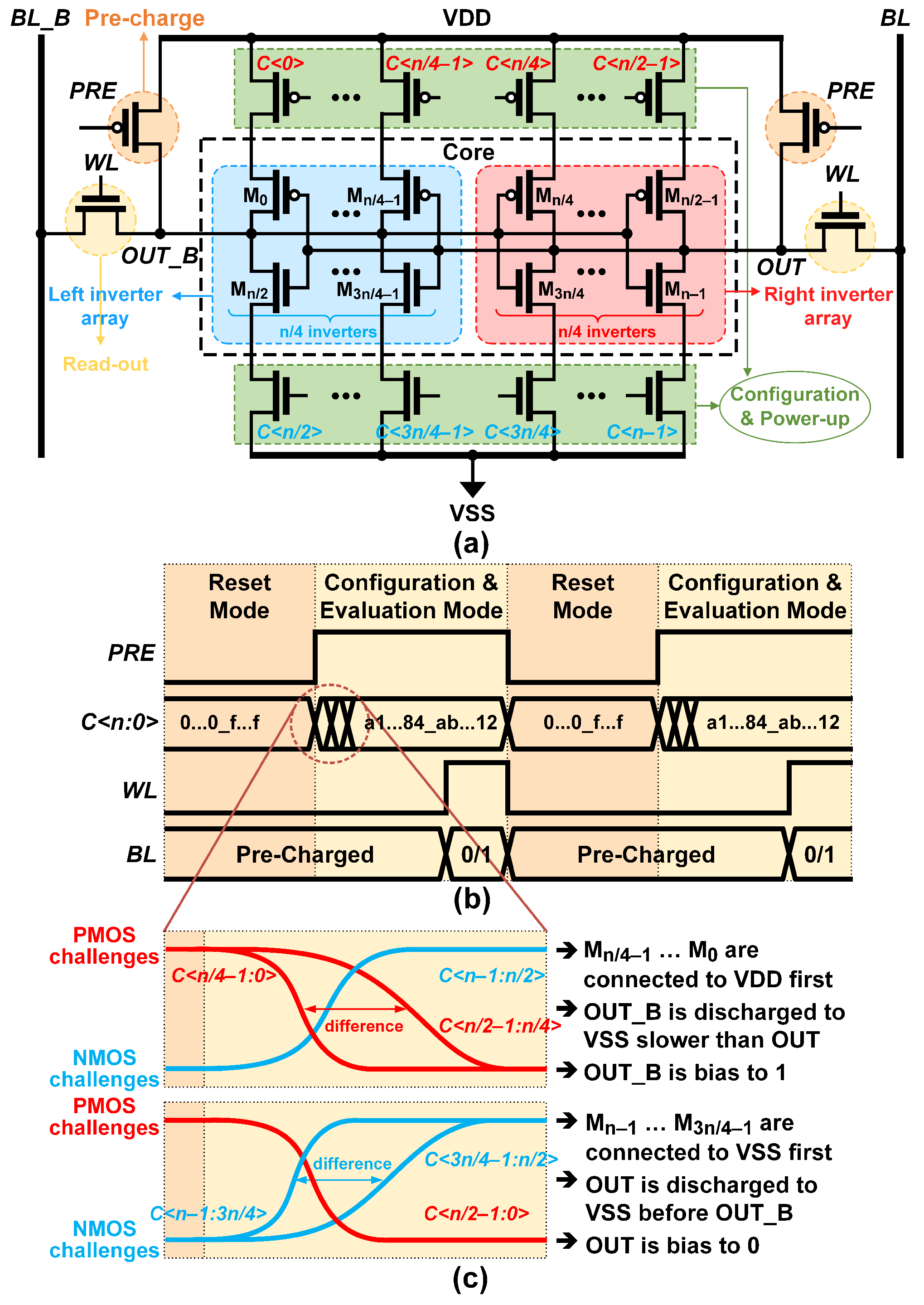
2. Conventional SRAM CRP PUF

2.1. Structure and Operation Principle

Figure 1a depicts the conventional structure of the PUF cell as described in [22]. Here, an n-bit challenge input signal, C<n−1:0>, is used to generate two opposing response outputs, BL and BL_B. Other signals such as PRE and WL ensure that the circuit is controlled corresponding to each operation mode. This structure is based on the 6T SRAM structure with two outputs, OUT and OUT_B. The core of this structure primarily comprises two inverter arrays positioned on the left and right sides. These two inverter arrays are interconnected to form a feedback loop, where the output of the left array connects to the input of the right array, and vice versa. Each array comprises n/4 identical inverters arranged in parallel. Each individual inverter within this array comprises a series of VDD pull-up transistors and a VSS pull-down transistor, which are activated by the challenge input. Thus, a 2-bit challenge input is applied to configure each inverter, an n/2-bit challenge input is applied to configure each inverter array, and an n-bit challenge input, C<n−1:0>, is applied to configure the PUF cell structure.
Each inverter array must be precisely configured to achieve a balance in the relative strengths of the VDD pull-ups and VSS pull-downs. Essentially, the number of ‘0’ bits in C<n/4−1:0> and C<n/2−1:n/4> must be identical to ensure a balanced connection to VDD between the two arrays. Similarly, the number of ‘1’ bits in C<3n/4−1:n/2> and C<n−1:3n/4> must be identical to maintain balanced connections to the VSS between the two arrays. This configuration ensures that the response generated by the PUF cell depends on the physical mismatch inherent to individual transistors, rather than a predetermined voltage generated from the imbalance strengths of the two arrays.
Figure 1b depicts the timing diagram for the PUF cell, which comprises two operating modes: “Pre-charge” and “Configuration & Evaluation”. In the “Pre-charge” mode, the PUF cell outputs are reset to the initial value, VDD, before the PUF cell state is set to generate new output values in the “Configuration & Evaluation” mode. During the “Pre-charge” mode, each inverter’s output voltages, OUT and OUT_B, are charged to VDD when an active low signal is applied to the PRE transistors. The bit-lines, BL and BL_B, are also set to VDD. Simultaneously, the NMOS challenges, C<n−1:n/2>, and PMOS challenges, C<n/2−1:0>, are set to low and high logic levels, respectively, to disconnect both the inverter arrays from the power supply. Following the “Pre-charge” mode, the PRE is high and the “Configuration & Evaluation” mode begins by applying an n-bit challenge input to configure the PUF cell while concurrently powering it up. Subsequently, the two cross-coupled inverter arrays compete with each other to determine the output logic level. The outputs are read to bit-lines when the word-line signal, WL, goes high.

2.2. Existing Issue

In this structure, achieving a response output from the inherent random process variations depends on balancing the two cross-coupled inverter arrays within the SRAM structure. However, obtaining this balance in the layout design is challenging due to inevitable mismatches [23], particularly in the signal lines connecting the arrays, potentially producing a biased output.
The challenge input signal serves dual roles, controlling the SRAM power-up and configuring the PUF cell. When a specific challenge input is applied, the specified challenge transistors are turned on to establish connections from the two arrays to the VDD and VSS. Power-up requires activating at least one bit among the n-bit challenges, while the configuration requires the activation of all the n-bit challenges. Disparities in parasitic components can cause the PUF cell to power up and decide its output value before all the challenge transistors are configured, causing incorrect operation during the “Configuration & Evaluation”.
The worst-case scenario involves activating the left PMOS challenge transistors before the right ones, and simultaneously activating all the NMOS challenge transistors, as shown in the upper part of Figure 1c. Since there is no timing difference among the NMOS transistors’ activations, the two outputs of the PUF cell are solely influenced by the activation times of the PMOS challenge transistors. The voltages, OUT_B and OUT, begin to drop from VDD simultaneously due to the current discharged to VSS when the NMOS challenge transistors are turned on. The voltage, OUT_B, decreases more slowly than the voltage, OUT, with the charge current to VDD since the left PMOS transistors are activated earlier. The instantaneous voltage difference between OUT_B and OUT is amplified by the positive feedback loop in the SRAM structure, and eventually, OUT_B is pulled up to VDD or deviates to 1. Conversely, if the right NMOS challenge transistors are turned on earlier than the left ones, all the PMOS transistors are turned on simultaneously, as shown in the lower part of Figure 1c. The two outputs of the PUF cell are only affected by the turn-on difference of the NMOS challenge transistors. The voltage, OUT, will be discharged to VSS before the voltage, OUT_B. Similarly, under the effect of a positive feedback loop, OUT is pulled down to VSS or biased towards zero. Thus, the PUF cell output depends on which challenge bit initiates the power-up earlier, rather than depending on the entire n-bit challenge input. Consequently, the PUF cell output becomes independent of the challenge input and produces a fixed response output. This can lead to a potential correlation between the response outputs corresponding to the different challenge inputs.
Similar to the challenge input, for the input signal PRE, asymmetrical connections to the two inverters result in one inverter being turned on earlier when PRE is set to a low level in the “Evaluation” mode. If any pre-charge transistor of the inverter array is turned off earlier, its output voltage will start to decrease from VDD before the other output. The positive feedback loop amplifies the instantaneous voltage difference between the two outputs, ultimately driving the output voltage of the inverter array, whose pre-charge transistor is turned off earlier, to zero. This also specifies a predetermined response output value even with distinct challenge inputs.
Meanwhile, reading the output voltage occurs when the input signal, WL, is high, activating the WL transistors to connect the two inverter outputs to the two bit-line outputs and altering the capacitance load value at the two inverter outputs. Turning on WL too early during a conflict between two inverter arrays in the “Evaluation” mode can affect the response output, and the mismatch between the two load capacitors can bias the response output to a predetermined value.

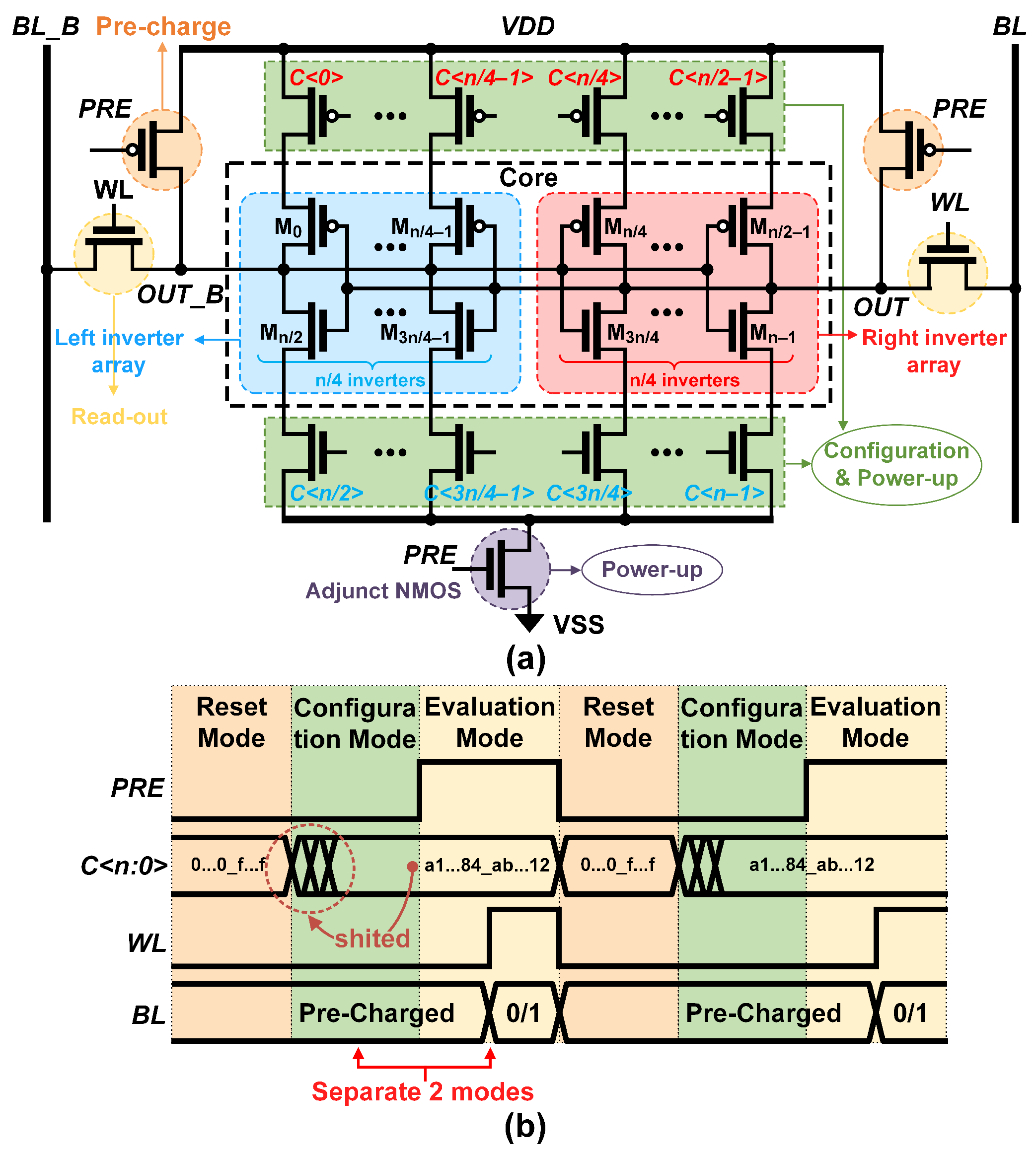
3. Proposed SRAM CRP PUF

3.1. Proposed Precise Timing Scheme for Ideal Random Response

Figure 2 depicts the proposed PUF cell structure and its timing diagram. The main objective is to eliminate the mismatch effect of the challenge input by exterminating its power-up function. Two revisions are introduced for this purpose. Firstly, a timing diagram revision is presented, as shown in Figure 2b, where the “Configuration & Evaluation” mode is divided into two separate modes. In the “Configuration” mode, the challenge input is set up to configure the PUF cell before the PRE signal becomes high. Subsequently, the two cross-coupled inverter arrays power up to compete with each other, determining the output logic level in the “Evaluation” mode. However, this revision results in the PUF outputs dropping during the challenge input setup due to the discharge current to the VSS through the NMOS challenge transistors. Thus, the PUF cell remains powered on in the “Configuration” mode even when the PRE signal is low. Consequently, a second revision is proposed. An adjunct NMOS transistor is added into the PUF cell structure, operating as power-up transistor, as shown in Figure 2a. This transistor is controlled by the PRE signal to disconnect the PUF cell from the VSS during the “Pre-charge” and “Configuration” modes; it then powers it up in the “Evaluation” mode. An appropriate sizing selection must be considered to provide an adequate current-carrying capability for this transistor. The size of this transistor must be sufficiently large to carry the maximum current when all the NMOS challenge transistors are turned on. Thus, the size of the PUF cell is increased compared to the conventional structure.
Additionally, the input signal, WL, is set to a high level after a sufficient time has elapsed since the start of the “Evaluation” mode to avoid capacitance load changes at the two inverter array outputs during their conflict. This ensures that the two outputs of the SRAM core exhibit fully diverse values before the data are read out to the bit-line.

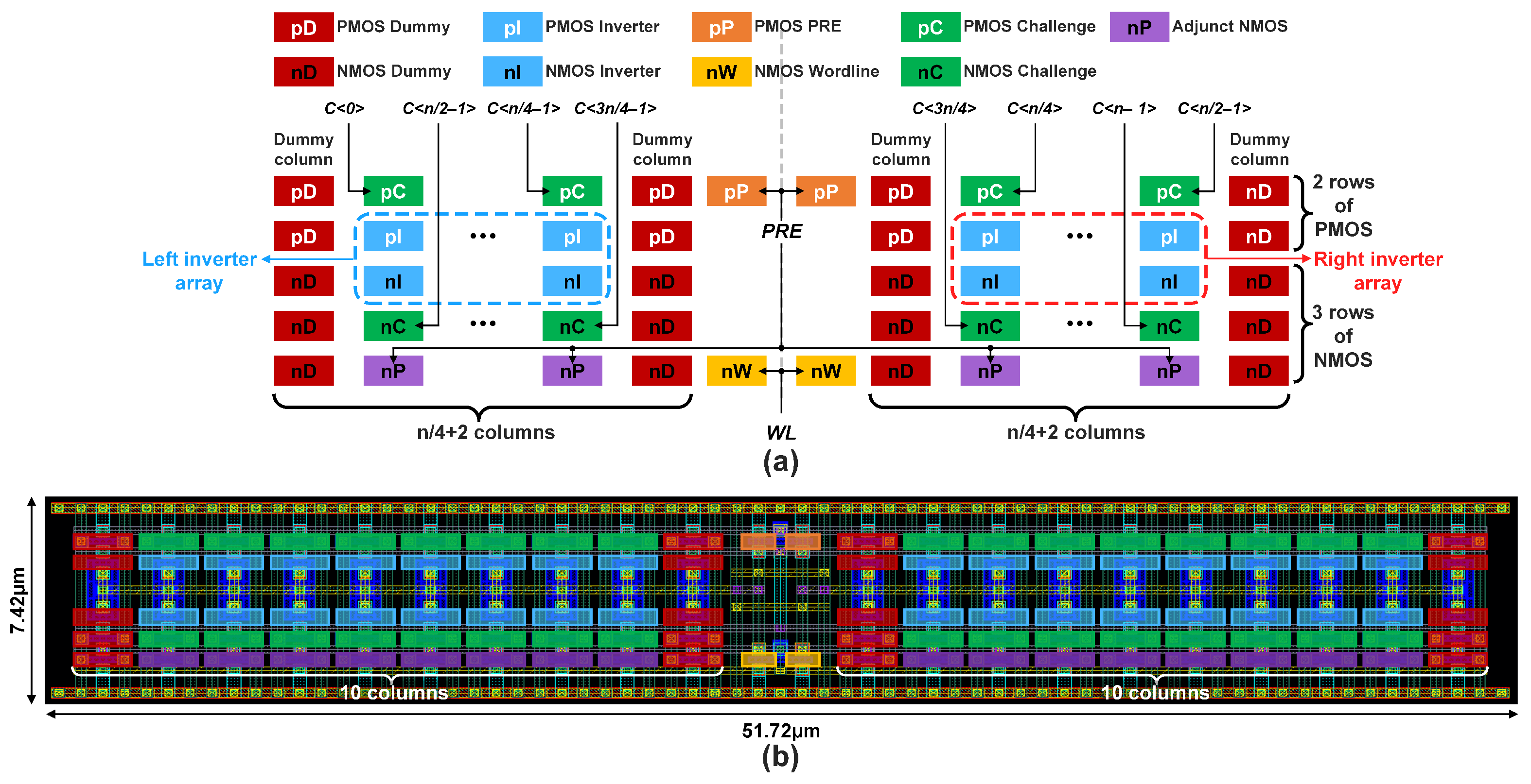
3.2. Symmetrical Layout Design Technique

In the realm of PUFs, two distinct forms of variation play a crucial role: systematic variation and random variation [24]. Systematic variation is predictable, and is caused by controlled manufacturing or environmental factors, while random variation is attributed to uncontrollable elements such as semiconductor manufacturing variations. Unlike systematic variations, random variations lack clear patterns due to their inherent unpredictability, contributing to the PUF security through entropy. To optimize randomness and reliability, the proposed PUF cell must utilize a regular layout, minimizing the systematic variations while maximizing the inherent device characteristics for enhanced local random variation. The symmetric layout of matched devices can help minimize systematic variations, and the use of small-sized devices will maximize variations in device characteristics, thereby enhancing the randomness and reliability of PUF [25].
Figure 3 depicts the layout implementation, illustrating the PUF cell floor plan, where the symmetric placement of both the inverter arrays is crucial for dominant random output characteristics inherited from process variation. This symmetrical arrangement minimizes the systematic variation [26]. Transistors within each inverter array are symmetrically placed based on the vertical boundary (dashed line). The transistors are placed as close together as possible to minimize the effects of gradients. The first n/4+2 and last n/4+2 transistor columns constitute the parallel-coupled inverters (blue color), the challenge transistors (green color), the adjunct NMOS transistors (purple color), and “dummy” transistors (red color) for the left and right sides, respectively. To ensure uniformity during silicon etching, two “dummy” columns are added, ensuring identical geometries for the transistors. Each column comprises five transistors that are stacked vertically, with two PMOS transistors at the top and three NMOS transistors at the bottom. The two middle columns are utilized for pre-charge transistors (orange color) at the top and word-line transistors (yellow color) at the bottom. The central space is designated for cross-wiring the outputs of the two inverter arrays.
Among the input lines connected to the left and right inverter transistors, the input signal, PRE, must be symmetrically connected to each array to simultaneously activate both inverters during the “Evaluation” mode. The input connection line of the PRE transistor must be connected symmetrically along the vertical boundary line to avoid delay mismatch. Meanwhile, the input signals, C<n−1:0> and WL, are conveniently connected to each array without the strict requirement of symmetry, because the proposed timing sets the challenge input in the “Configuration” mode, which does not impact PUF operation in “Evaluation” mode. The world-line is activated after a sufficient wait time in the proposed timing scheme, ensuring the two PUF outputs are fully polarized to opposite values.
The layout design for the PUF cell requires an area of 7.42 μ m × 51.72 μ m, utilizing the 180 nm CMOS process shown in Figure 3b. The transistors are set to the minimum size, W/L = 220 nm/180 nm, to maximize the random variation (local mismatch) [27]. With a bit-width of n = 32 for the input challenge signal, the design incorporates a total of 104 transistors. The actual layout organizes transistors according to a floorplan, utilizing assigned colors to represent distinct functions.

3.3. Simulation Results Comparison

To evaluate the effectiveness of the proposed approach when compared to the conventional SRAM CRP PUF, we conducted simulations to analyze the impact of switching delay differences on the PUF cell output. The randomness of the PUF output is achieved using Monte Carlo simulation on the Cadence Virtuoso tool. The characteristics of each transistor, including parameters such as channel length, channel width, oxide layer thickness, etc., were modeled with random variations reflective of the manufacturing process, generating 1000 data points. Output responses were then gathered by applying a predefined set of 10 specific challenge inputs to a PUF cell.
Figure 4 presents the simulation results. In a conventional SRAM CRP PUF, the ‘1’ ratio at the PUF cell output has a mean of 65.32% and a standard deviation of 0.4962% for post-simulation with the presence of delay mismatches in the layout design. For the proposed SRAM CRP PUF cell, the average value is 46.06% and the standard deviation is 1.0113%. The largest deviation from the ideal value is 4.8%, presenting a decrease of approximately 3.4 times when compared to the simulation result of the conventional structure of 16.4%. This simulation outcome clearly demonstrates that the proposed approach improves the randomness of the PUF output.
The output randomness can be considered further based on predicting the output according to the threshold voltage mismatch from [28], which can be expressed as follows:
M F = W F . Δ P ( 1 W F ) . Δ N
where M F is the mismatch metric used to predict the output value OUT; W F is the weight factor applied to each mismatch component, accounting for the intrinsic differences between PMOS and NMOS transistors; Δ P is the threshold voltage mismatch between PMOS transistors of the left and right inverter arrays; Δ N is the threshold voltage mismatch between NMOS transistors of the left and right inverter arrays in Figure 1a.
In the absence of a delay mismatch, the predicted output is a random value (‘1’ or ‘0’) due to its dependence only on the threshold voltage mismatches Δ P and Δ N . If Δ P Δ N , then M F > 0 , indicating the predicted output is ‘1’. Conversely, if Δ P Δ N , thus M F < 0 , hence the predicted output is ‘0’. However, the presence of delay mismatch in the layout design, as presented in Section 2.2, results in the output depending not only on the threshold voltage mismatch but also on the delay mismatch of the control signal lines. Consequently, the PUF output will be biased more towards ‘1’ or ‘0’ and the ratio of ‘1’ or ‘0’ at the output will deviate from the ideal value of 50%. By using the proposed method, the dependence of the output on the control signal lines is eliminated, and the output randomness can be maintained in Equation (1).

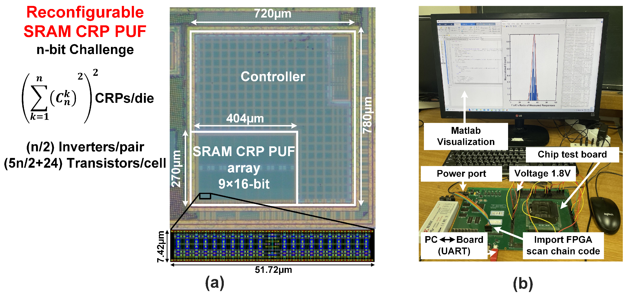
4. Implementation of SRAM CRP PUF System

Figure 5 depicts the mixed-signal system architecture, an Application-Specific Integrated Circuit (ASIC) consisting of two blocks: a digital controller and an analog SRAM CRP PUF array (9 × 16-bit). The digital controller was designed using the Synopsys tool, while the analog SRAM CRP PUF array and the integration of these two blocks were implemented using the Cadence Virtuoso tool. The controller generates signals to control the operation of each PUF cell with the state control unit block designed to follow the proposed timing revision. The counter block is used to select each row in the PUF array and count the clock cycle to generate the corresponding control signals, EN_BL, PRE<8:0>, EN<8:0>, C<n−1:0>, and WL<8:0>. The 9 × 16-bit SRAM CRP PUF array is divided into two parts: the upper part and the lower part. Each part comprises 9 rows and 8 columns of PUF cells, resulting in a 72-bit response. In each column, two tristate buffers are connected to the two outputs of each PUF cell to read the response output. The 1-bit response is obtained from one output among two tristate buffers. The 16-bit response per row is the final response output, PUF_OUT<15:0>.

5. Measurement Result

5.1. Evaluation Setup
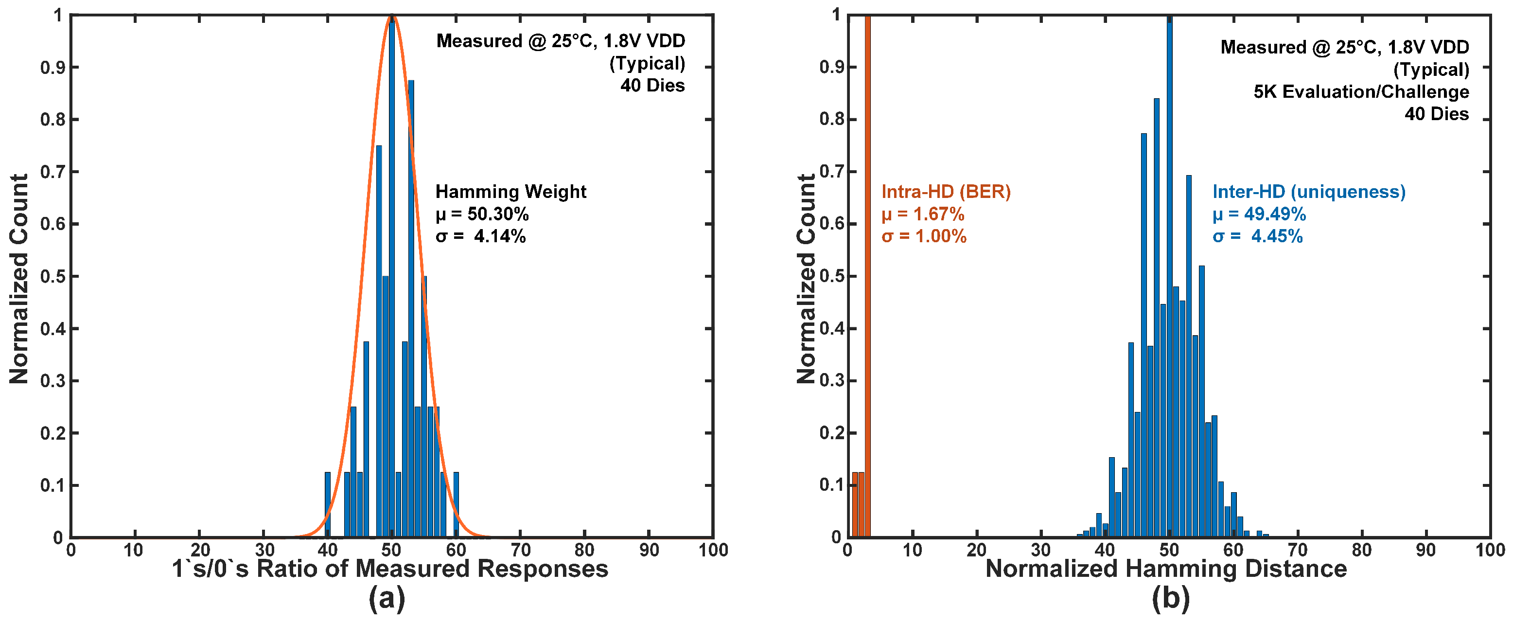
The proposed PUF was implemented by using a 180 nm CMOS process. The die microphotograph is shown in Figure 6a. The PUF has an area of 720 μ m × 780 μ m with the core PUF occupying 404 μ m × 270 μ m. Figure 6b depicts the measurement setup to verify the performance of the PUF, where a chip test board with a Xilinx FPGA and a memory scan chain for massively iterative testing are used to establish the experimental environment. The PUF operates at a frequency of 20 MHz under the conditions of a supply voltage of 1.8 V and a temperature of 25 °C. In this paper, the PUF’s performance is analyzed through various metrics, including the Hamming weight, inter and intra Hamming distance, and auto-correlation function (ACF). Lastly, the chip performance is compared with the state-of-the-art PUF structures.

5.2. Hamming Weight

The Hamming weight illustrates the distribution of ‘1’s and ‘0’s in the PUF response [29]. Figure 7a presents the Hamming weight distribution across 40 PUF instances with a specific challenge. The results demonstrate a mean of 50.30% with a standard deviation of 4.14%, indicating that it closely approaches the ideal value of 50%. This measurement result is much better than the simulation value due to the integration of more process variations from an array of 144 PUF cells, whereas the simulation only considers a single PUF cell. Additionally, this measurement result is the best value that we achieved with various challenge inputs.

5.3. Inter and Intra Hamming Distance

Both inter and intra Hamming distance analyses were performed to comprehensively evaluate the uniqueness and stability of the PUF [30]. The inter-HD quantifies the Hamming distance between responses obtained from 40 different PUF instances. Conversely, the intra-HD measures the Hamming distance between responses acquired from the same PUF cell across 5000 trials. Figure 7b depicts the histogram, which shows that the measured inter-HD is 0.4949 with a standard deviation of 0.0445. This inter-HD value indicates a high level of distinctiveness among the PUF cells. Additionally, the measured intra-HD is 0.0167 with a standard deviation of 0.01, indicating consistently reliable responses from the same PUF cell over time. These results highlight the robustness of the PUF, making it a dependable and stable hardware security component for various applications.

5.4. Auto-Correlation Function

The ACF analysis is crucial for assessing the correlation between the PUF responses at different bit positions [31]. The spatial autocorrelation of the 120,000-bit response is measured to be within ±0.00557 at a 95% confidence interval (CI), as shown in Figure 8c. The ACF has a waveform and exceeds the CI in the worst case of delay mismatch, as shown in Figure 8a. When compared to [22], the ACF of the proposed structure is more concentrated in the CI, especially at low lags. This demonstrates that the proposed structure provides independent and unique responses.

5.5. Performance Comparison

Table 1 presents the comparison results with state-of-the-art strong PUFs. This design achieves a small area of 1.2 × 10 4 F 2 /bit and power consumption of 7 pJ/bit. For a fair evaluation, the table includes normalized core area and power consumption metrics. The normalized area is calculated by linearly normalizing to the challenge bit width. The normalized power consumption is calculated by dividing by the minimum gate length of the CMOS process raised to the power of three and the challenge bit width. In Table 1, our proposed PUF consumes 4 times more power than [22] and 3.7 times more power than [32]. However, when considering the same operating frequency of 20 MHz, the proposed PUF’s power consumption compared to [22] is nearly equivalent. Ref. [33] uses transistors operating in the subthreshold region, so it consumes 2.06 times less power than the proposed structure. Additionally, the power consumption of the proposed structure is also 2.05 times better than [33]. The area per bit is significantly smaller than [33,34], less than half the size of [22] but larger than [32], as more transistors were used. This design achieves the lowest worst-case BER of 4.86%. The Inter-HD value of 0.4949 is close to the ideal value of 0.5 when compared to most other PUFs except [33,34] and the intra-HD is the most comparable with those of other PUFs. Overall, the proposed PUF exhibits a good balance between the inter-HD value, intra-HD value, and area efficiency. A direct comparison with conventional reconfigurable SRAM CRP PUF demonstrates that our design presents the reliability and randomness, since it incorporates a larger number of transistors. Furthermore, our design achieves a smaller area per bit when compared to the conventional method by adopting a symmetric layout technique.

6. Conclusions

In this paper, we proposed a novel reconfigurable SRAM CRP PUF that achieves high reliability and randomness. We propose an operation timing control scheme, incorporating an adjunct NMOS transistor, to eliminate the challenge and word-line input mismatch. Additionally, we introduce symmetric layout techniques to achieve ideal random response bits. The symmetric arrangement of the two inverter arrays maximizes the inherent random output characteristic inherited from process variation, and the pre-charge input signal must be connected symmetrically to each array to avoid a delay mismatch. The proposed PUF is fabricated through a 180 nm CMOS process, and achieves a compact cell area of 1.2 × 10 4 F 2 /bit. Across 40 chips, the inter-HD measured at 0.4949, with an intra-HD of 0.0167 in a single chip across 5000 trials. Notably, the worst-case BER stands at only 4.86%. The proposed PUF exhibits good reliability and randomness characteristics, along with a compact silicon area, when compared to other state-of-the-art designs. Future efforts should explore pre-processing and post-processing techniques to enhance the reliability of the method.

Author Contributions

Conceptualization, J.-P.H.; methodology, J.-P.H.; software, V.K.P.; validation, V.K.P.; formal analysis, V.K.P.; investigation, V.K.P.; resources, V.K.P. and J.-P.H.; data curation, V.K.P. and J.-P.H.; writing—original draft preparation, V.K.P.; writing—review and editing, V.K.P., C.T.N., J.-W.N. and J.-P.H.; visualization, V.K.P., C.T.N. and J.-W.N.; supervision, J.-P.H.; project administration, J.-P.H.; funding acquisition, J.-P.H. All authors have read and agreed to the published version of the manuscript.

Funding

This research was supported by Basic Science Research Program through the National Research Foundation of Korea (NRF) funded by the Ministry of Education (No. 2020R1A6A1A12047945). This research was also supported by Mid-Career Researcher Program through the National Research Foundation of Korea (NRF) funded by the MSIT (Ministry of Science and ICT) (NRF-2021R1A2C2005258).

Data Availability Statement

The data presented in this study are available on request from the corresponding author.

Acknowledgments

The chip fabrication and EDA tool were supported by the IC Design Education Center (IDEC), Republic of Korea.

Conflicts of Interest

The authors declare no conflicts of interest.

References

  1. Yang, Y.; Wu, L.; Yin, G.; Li, L.; Zhao, H. A survey on security and privacy issues in Internet-of-Things. IEEE Internet Things J. 2017, 4, 1250–1258. [Google Scholar] [CrossRef]
  2. Williams, P.; Dutta, I.K.; Daoud, H.; Bayoumi, M. A survey on security in Internet of Things with a focus on the impact of emerging technologies. Internet Things 2022, 19, 100564. [Google Scholar] [CrossRef]
  3. Ngo, C.T.; Eshraghian, J.K.; Hong, J.P. An Area-Optimized and Power-Efficient CBC-PRESENT and HMAC-PHOTON. Electronics 2022, 11, 2380. [Google Scholar] [CrossRef]
  4. Manifavas, C.; Hatzivasilis, G.; Fysarakis, K.; Rantos, K. Lightweight cryptography for embedded systems–A comparative analysis. In International Workshop on Data Privacy Management; Springer: Berlin/Heidelberg, Germany, 2013; pp. 333–349. [Google Scholar]
  5. Herder, C.; Yu, M.D.; Koushanfar, F.; Devadas, S. Physical Unclonable Functions and Applications: A Tutorial. Proc. IEEE 2014, 102, 1126–1141. [Google Scholar] [CrossRef]
  6. Choi, K.U.; Baek, S.; Heo, J.; Hong, J.P. A 100% stable sense-amplifier-based physically unclonable function with individually embedded non-volatile memory. IEEE Access 2019, 8, 21857–21865. [Google Scholar] [CrossRef]
  7. Shamsoshoara, A.; Korenda, A.; Afghah, F.; Zeadally, S. A survey on physical unclonable function (PUF)-based security solutions for Internet of Things. Comput. Netw. 2020, 183, 107593. [Google Scholar] [CrossRef]
  8. Hu, Y.W.; Zhang, T.P.; Wang, C.F.; Liu, K.K.; Sun, Y.; Li, L.; Lv, C.F.; Liang, Y.C.; Jiao, F.H.; Zhao, W.B.; et al. Flexible and biocompatible physical unclonable function anti-counterfeiting label. Adv. Funct. Mater. 2021, 31, 2102108. [Google Scholar] [CrossRef]
  9. Kursawe, K.; Sadeghi, A.R.; Schellekens, D.; Skoric, B.; Tuyls, P. Reconfigurable physical unclonable functions-enabling technology for tamper-resistant storage. In Proceedings of the 2009 IEEE International Workshop on Hardware-Oriented Security and Trust, San Francisco, CA, USA, 27 July 2009; IEEE: Piscataway, NJ, USA, 2009; pp. 22–29. [Google Scholar]
  10. Esidir, A.; Kiremitler, N.B.; Kalay, M.; Basturk, A.; Onses, M.S. Unclonable Features via Electrospraying of Bulk Polymers. ACS Appl. Polym. Mater. 2022, 4, 5952–5964. [Google Scholar] [CrossRef]
  11. Ibrahim, O.A.; Sciancalepore, S.; Di Pietro, R. MAG-PUF: Magnetic Physical Unclonable Functions for Device Authentication in the IoT. In Proceedings of the International Conference on Security and Privacy in Communication Systems, Virtual Event, 17–19 October 2022; Springer: Berlin/Heidelberg, Germany, 2022; pp. 130–149. [Google Scholar]
  12. Konigsmark, S.C.; Hwang, L.K.; Chen, D.; Wong, M.D. CNPUF: A carbon nanotube-based physically unclonable function for secure low-energy hardware design. In Proceedings of the 2014 19th Asia and South Pacific Design Automation Conference (ASP-DAC), Singapore, 20–23 January 2014; IEEE: Piscataway, NJ, USA, 2014; pp. 73–78. [Google Scholar]
  13. Lu, X.; Hong, L.; Sengupta, K. 15.9 An integrated optical physically unclonable function using process-sensitive sub-wavelength photonic crystals in 65nm CMOS. In Proceedings of the 2017 IEEE International Solid-State Circuits Conference (ISSCC), San Francisco, CA, USA, 5–9 February 2017; IEEE: Piscataway, NJ, USA, 2017; pp. 272–273. [Google Scholar]
  14. Taneja, S.; Alvarez, A.B.; Alioto, M. Fully synthesizable PUF featuring hysteresis and temperature compensation for 3.2% native BER and 1.02 fJ/b in 40 nm. IEEE J. Solid-State Circuits 2018, 53, 2828–2839. [Google Scholar] [CrossRef]
  15. McGrath, T.; Bagci, I.E.; Wang, Z.M.; Roedig, U.; Young, R.J. A PUF taxonomy. Appl. Phys. Rev. 2019, 6, 11303. [Google Scholar] [CrossRef]
  16. Che, W.; Saqib, F.; Plusquellic, J. PUF-based authentication. In Proceedings of the 2015 IEEE/ACM International Conference on Computer-Aided Design (ICCAD), Austin, TX, USA, 2–6 November 2015; IEEE: Piscataway, NJ, USA, 2015; pp. 337–344. [Google Scholar]
  17. Chen, Q.; Csaba, G.; Lugli, P.; Schlichtmann, U.; Rührmair, U. The bistable ring PUF: A new architecture for strong physical unclonable functions. In Proceedings of the 2011 IEEE International Symposium on Hardware-Oriented Security and Trust, San Diego, CA, USA, 5–6 June 2011; IEEE: Piscataway, NJ, USA, 2011; pp. 134–141. [Google Scholar]
  18. Delavar, M.; Mirzakuchaki, S.; Mohajeri, J. A ring oscillator-based PUF with enhanced challenge-response pairs. Can. J. Electr. Comput. Eng. 2016, 39, 174–180. [Google Scholar] [CrossRef]
  19. Govindaraj, R.; Ghosh, S.; Katkoori, S. Design, analysis and application of embedded resistive RAM based strong arbiter PUF. IEEE Trans. Dependable Secur. Comput. 2018, 17, 1232–1242. [Google Scholar] [CrossRef]
  20. He, Z.; Wan, M.; Deng, J.; Bai, C.; Dai, K. A reliable strong PUF based on switched-capacitor circuit. IEEE Trans. Very Large Scale Integr. (VLSI) Syst. 2018, 26, 1073–1083. [Google Scholar] [CrossRef]
  21. Cao, Y.; Liu, C.Q.; Chang, C.H. A low power diode-clamped inverter-based strong physical unclonable function for robust and lightweight authentication. IEEE Trans. Circuits Syst. I Regul. Pap. 2018, 65, 3864–3873. [Google Scholar] [CrossRef]
  22. Baek, S.; Yu, G.H.; Kim, J.; Ngo, C.T.; Eshraghian, J.K.; Hong, J.P. A reconfigurable SRAM-based CMOS PUF with challenge to response pairs. IEEE Access 2021, 9, 79947–79960. [Google Scholar] [CrossRef]
  23. Nam, J.W.; Kim, J.; Hong, J.P. Stochastic Cell-and Bit-Discard Technique to Improve Randomness of a TRNG. Electronics 2022, 11, 1735. [Google Scholar] [CrossRef]
  24. Agarwal, K.; Nassif, S. Characterizing process variation in nanometer CMOS. In Proceedings of the 44th Annual Design Automation Conference, San Diego, CA, USA, 4–8 June 2007; pp. 396–399. [Google Scholar]
  25. Bhargava, M.; Mai, K. An efficient reliable PUF-based cryptographic key generator in 65 nm CMOS. In Proceedings of the 2014 Design, Automation & Test in Europe Conference & Exhibition (DATE), Dresden, Germany, 24–28 March 2014; IEEE: Piscataway, NJ, USA, 2014; pp. 1–6. [Google Scholar]
  26. Hastings, A. The Art of Analog Layout; Prentice-Hall Inc.: Upper Saddle River, NJ, USA, 2001. [Google Scholar]
  27. Drennan, P.G.; McAndrew, C.C. Understanding MOSFET mismatch for analog design. IEEE J. Solid-State Circuits 2003, 38, 450–456. [Google Scholar] [CrossRef]
  28. Alheyasat, A.; Torrens, G.; Bota, S.A.; Alorda, B. Estimation during design phases of suitable SRAM cells for PUF applications using separatrix and mismatch metrics. Electronics 2021, 10, 1479. [Google Scholar] [CrossRef]
  29. Schrijen, G.J.; Van Der Leest, V. Comparative analysis of SRAM memories used as PUF primitives. In Proceedings of the 2012 Design, Automation & Test in Europe Conference & Exhibition (DATE), Dresden, Germany, 12–16 March 2012; IEEE: Piscataway, NJ, USA, 2012; pp. 1319–1324. [Google Scholar]
  30. Barbareschi, M.; Battista, E.; Mazzeo, A.; Mazzocca, N. Testing 90 nm microcontroller SRAM PUF quality. In Proceedings of the 2015 10th International Conference on Design & Technology of Integrated Systems in Nanoscale Era (DTIS), Napoli, Italy, 21–23 April 2015; IEEE: Piscataway, NJ, USA, 2015; pp. 1–6. [Google Scholar]
  31. Böhm, C.; Hofer, M.; Pribyl, W. A microcontroller SRAM-PUF. In Proceedings of the 2011 5th International Conference on Network and System Security, Milan, Italy, 6–8 September 2011; IEEE: Piscataway, NJ, USA, 2011; pp. 269–273. [Google Scholar]
  32. Nam, J.W.; Ahn, J.H.; Hong, J.P. Compact SRAM-based PUF chip employing body voltage control technique. IEEE Access 2022, 10, 22311–22319. [Google Scholar] [CrossRef]
  33. Venkatesh, A.; Venkatasubramaniyan, A.B.; Xi, X.; Sanyal, A. 0.3 pJ/bit machine learning resistant strong PUF using subthreshold voltage divider array. IEEE Trans. Circuits Syst. II Express Briefs 2019, 67, 1394–1398. [Google Scholar] [CrossRef]
  34. Zhuang, H.; Xi, X.; Sun, N.; Orshansky, M. A strong subthreshold current array PUF resilient to machine learning attacks. IEEE Trans. Circuits Syst. I Regul. Pap. 2019, 67, 135–144. [Google Scholar] [CrossRef]
Figure 1. (a) Unit cell schematic of conventional SRAM CRP PUF, (b) its operational timing diagram, and (c) Switching delay difference of challenge.
Electronics 13 00309 g001
Figure 2. (a) Unit cell schematic of the proposed SRAM CRP PUF and (b) its operational timing diagram.
Electronics 13 00309 g002
Figure 3. (a) Layout floor plan and (b) Layout design with 32-bit challenge input.
Electronics 13 00309 g003
Figure 4. Simulation results of the conventional and proposed SRAM CRP PUF.
Electronics 13 00309 g004
Figure 5. SRAM CRP PUF system architecture.
Electronics 13 00309 g005
Figure 6. (a) Die microphotograph of the proposed SRAM CRP PUF and (b) Overall chip measurement environment.
Electronics 13 00309 g006
Figure 7. (a) Measured Hamming weight distribution and (b) measured Inter/Intra-PUF Hamming distance distribution.
Electronics 13 00309 g007
Figure 8. ACF measured with 120,000-bit of (a) Worst case of delay mismatch (b) conventional SRAM CRP PUF and (c) Proposed SRAM CRP PUF.
Electronics 13 00309 g008
Table 1. Comparison with state-of-the-art strong PUFs.
This Work[22][32][33][34]
Technology (nm)180656565130
Bit-Width of Challenge (bit)3232326065
Type of PUFReconf. SRAMReconf. SRAMSRAMVoltage ArraySCA
Possible CRPs1.6 × 10 8 1.6 × 10 8 1.6 × 10 8 1.15 × 10 18 3.7 × 10 19
Worst-case BER4.86%13.7%20.8%10.9%9%
Area/bit (F 2 /bit)1.2 × 10 4 2.1 × 10 4 0.9 × 10 4 66.3 × 10 4 55.0 × 10 4
Normalized Area *11.750.7529.4727.08
Energy/bit (pJ/b)70.0820.090.311
Normalized Energy **10.250.270.4852.05
Inter-HD0.49490.48930.48890.50260.499
Intra-HD0.01670.0240.03110.04660.058
* Normalized with challenge bit-width; ** Normalized with CMOS technology and challenge bit-width.
Disclaimer/Publisher’s Note: The statements, opinions and data contained in all publications are solely those of the individual author(s) and contributor(s) and not of MDPI and/or the editor(s). MDPI and/or the editor(s) disclaim responsibility for any injury to people or property resulting from any ideas, methods, instructions or products referred to in the content.

