1. Introduction
A successful energy transition requires new strategies and careful planning to integrate all new technologies and devices for the production and storage of electrical energy. This is what some authors call “smart electrification” [
1]. In this regard, electric vehicles (EVs) play a relevant role. When electric vehicles are parked and plugged-in, they can supply power to the grid or the owner’s home to meet demand peaks in what are known as vehicle-to-grid (V2G) or vehicle-to-home (V2H) strategies. Additionally, the energy stored in their batteries can help to regulate both the voltage and frequency on the grid. To achieve these capabilities, it is necessary that the converters that connect the grid with the EVs allow the bidirectional flow of energy [
2].
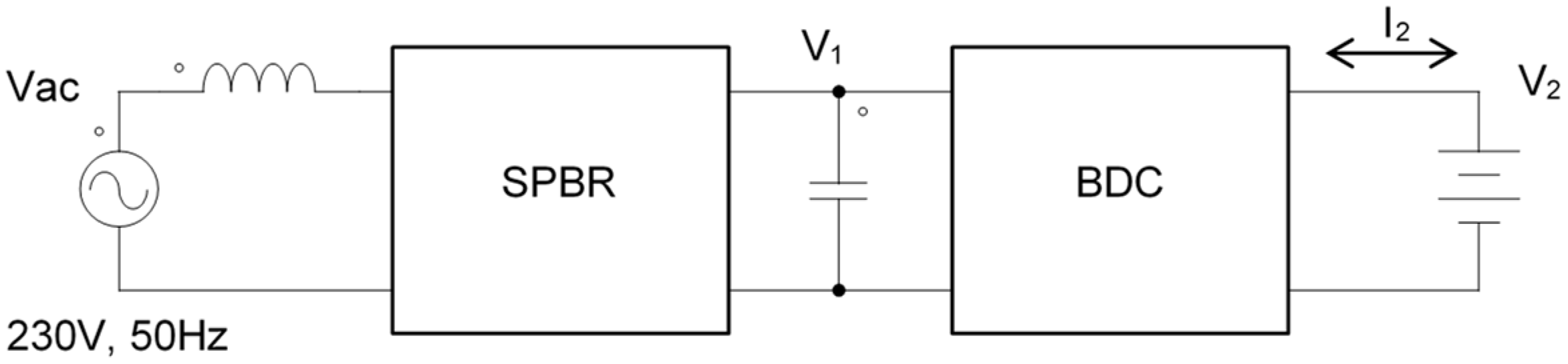
Figure 1 shows a diagram that describes the mentioned solution for the case of a single-phase 230 V AC mains supply. The SPBR (single phase bidirectional rectifier) block is connected to the power grid through an inductance. The BDC (bidirectional DC–DC converter) block connects the EV battery to the DC link capacitor. The electronic control of the complete converter allows us to regulate the amplitude and direction of the current
I2 for the given values of the SPBR output voltage
V1 and nominal battery voltage
V2. In a conventional battery charging process, the current
I2 flows from the network to the battery. When the battery energy is used to supply power to the grid, the direction of
I2 is the opposite [
3]. It is also possible to integrate renewable energy systems and bidirectional EV chargers to facilitate smart electrification and reduce net operating costs by providing grid support and using the EV battery as a power reserve [
4].
The typical topology for the SPBR block consists of a conventional transistorized single-phase full bridge boost rectifier with a pulse width modulation controlled by the input current and output voltage operating at a unity power factor and with power reversal capability [
5,
6]. For three-phase mains, the preferred solution adopted is based on full bridges of three transistor legs [
7,
8].
The most immediate solution for the BDC consists of a simple bidirectional DC/DC converter [
9], but for safety reasons, this converter must have galvanic isolation; these are the isolated bidirectional DC–DC converters (IBDC). The most accepted solution is a converter that uses two full bridges of transistors (dual active bridges—DABs) [
10] or two half-bridges (dual active half-fridges—DAHBs) [
11] connected so that the output of one is the input of the other. For large power levels, this topology can be optimized by using multiphase DABs [
12]. One way to improve efficiency and electromagnetic interference (EMI) emission is the use of resonant DABs [
13] or by means of broadband devices such as silicon carbide (SiC) [
14] and gallium nitride (GaN) [
15].
In DABs, the control and direction of the flow of the transferred power is carried out by shifting the operation of each of the bridges through different control techniques: single phase shift SPS [
16], extended phase shift EPS [
17], dual phase shift DPS [
18] and triple phase shift TPS [
19]. All of them are modifications of the SPS method to improve the transmission power capacity and the efficiency of the converter maintaining the zero voltage switch (ZVS) condition and minimizing the circulating current.
To achieve further improvements, hybrid control techniques are used where the DAB is controlled by phase shifting and variable frequency modulations, in sequential or independent mode, to extend the operating range of the converter while maintaining ZVS conditions [
20,
21] or introducing a circulating current suppression control (CCSC) that affects the DAB power transfer [
22]. Ref. [
23] proposes the use of a variable frequency control strategy plus an additional control loop to find the point of maximum efficiency for medium frequency (25 kHz). Other authors use variable frequency in a series resonant dual active bridge (SR-DAB) [
24] or combining it with triple phase shift (VF-TPS) [
25]. In order to further develop the study of these hybrid control techniques, this paper describes a variable frequency non-resonant isolated bidirectional DAB DC–DC converter (VF-IBDC) based on SiC MOSFET transistors operating at high frequency that combines SPS and VF modulations simultaneously so that the switching processes are carried out at zero voltage and also at zero current switching (ZCS) conditions in a wide operating range. In this way, high efficiency peaks, close to 99%, can be obtained with moderate EMI.
The paper is structured as follows:
Section 2 focuses on the configuration of the proposed IBDC converter. In
Section 3, an analysis of the conventional SPS-IBDC converter is conducted, followed by the analysis and design considerations for the proposed modulation in
Section 4.
Section 5 presents the comparative analysis of power losses and efficiency of the converters. In
Section 6, the proposed VF-IBDC control method is introduced. The validation of results using experimental data is presented in
Section 7. Finally, the conclusions are drawn.
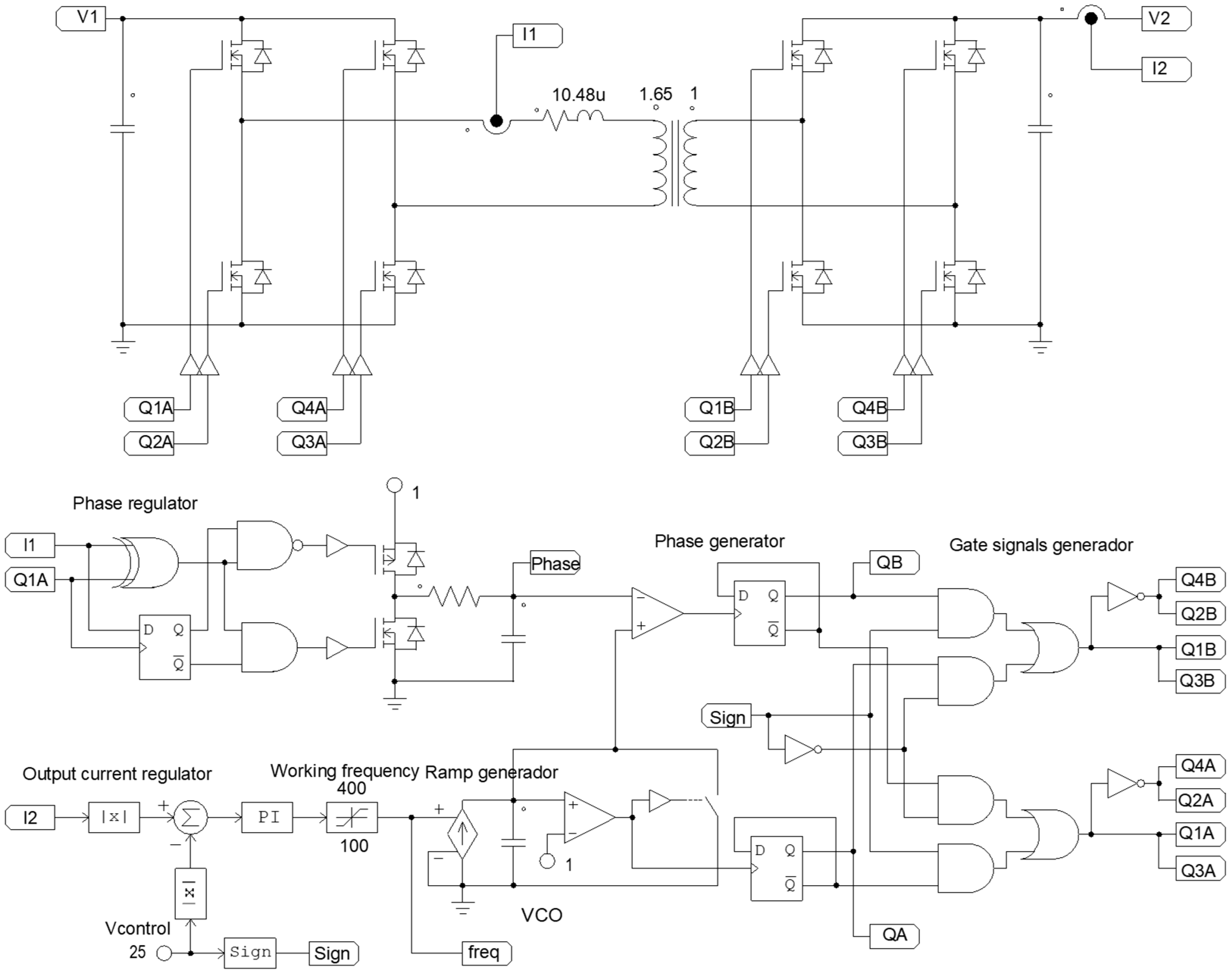
2. IBDC Configuration
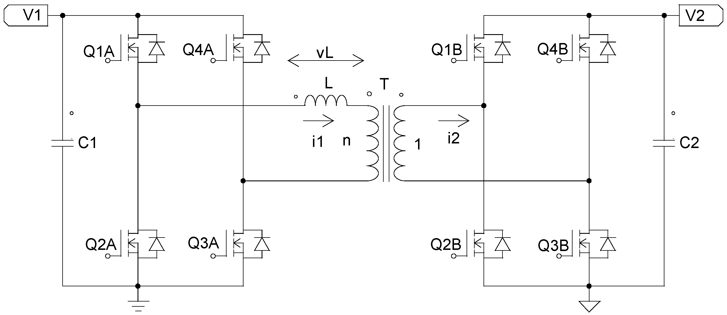
Figure 2 shows the simplified schematic of the DAB-IBDC converter which consists of two full bridges with active switches in the primary and the secondary sides, connected via the high-frequency transformer T that provides the required galvanic isolation and voltage matching between two voltage levels
V1 and
V2. The inductor L, which also includes the leakage inductance of the transformer, serves as the instantaneous energy storage device. The duty ratio of the switching signal is 50%, but there is a phase shift
ϕ between primary and secondary bridges that defines the amplitude and direction of the power flow. C1 is the DC link capacitor connected to the output voltage
V1 of the SPBR and C2 is the output capacitor of the DAB-IBDC. In this point of voltage
V2, the EV battery is connected. In charge mode, the power flows from C1 to C2. When the battery supplies power to the grid (discharge mode), the power flows in the opposite direction. All transistors are SiC MOSFET.
The design has been made for a fast bidirectional charging application of lithium-ion EV batteries using a typical conventional charging process [
26].
Table 1 shows several values that serve as specifications for the converter design. When the converter delivers maximum power in the first phase of the charging process, the output current must be regulated independently of the existing battery voltage.
3. Analysis of the SPS-IBDC
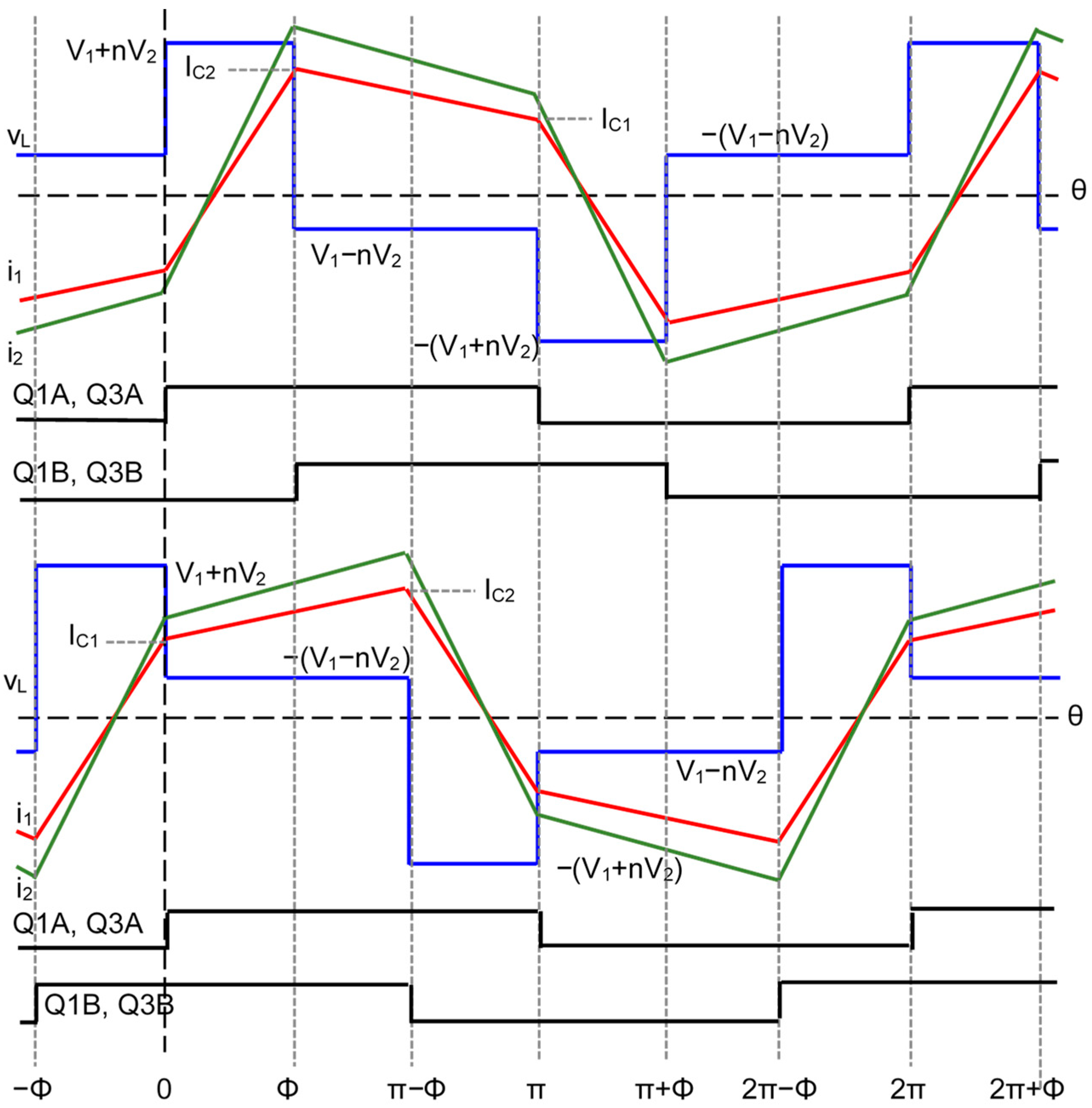
Figure 3 shows the main simplified waveforms of the SPS-IBDC in charge mode (top) and discharge mode (bottom). The black waveforms are the switching signals of transistor Q1A and Q3A in the primary bridge, and Q1B and Q3B in the secondary bridge. The switching signals of Q2A and Q4A, and Q2B and Q4B are delayed by 180°. All of these signals are shown as square signals (with duty cycle D = 0.5) because dead time was not considered to simplify the graph. The blue waveforms represent the voltage across the inductance L, the red waveforms show the output current of the primary bridge, and the green waveforms are the input current of the secondary bridge. Note that the sign of
ϕ determines the mode of operation so that if
ϕ is positive, the converter acts in charge mode, and if
ϕ is negative, it acts in discharge mode.
To extract properties and be able to design the circuit, it is necessary to carry out a complete analysis to obtain the equations that describe the behavior of its voltages and currents. The aim is to obtain a single set of equations that can describe the circuit in charging or discharging operating mode at the same time. The observation of the similarities and differences of the voltage waveforms in the inductance allows us to define two new parameters,
δ and
V2*, given by
After this, the voltage
vL(
θ) of the inductance and the output current of the primary bridge
i1(
θ) for any operating cycle can be determined by means of next piecewise equations:
with
ω = 2
πf where
f is the switching frequency. Integrating the square of (3) and (4), it is possible to calculate the corresponding root mean square (rms) values:
and the values of the switching currents can be obtained:
The value of the active power transferred between the primary and the secondary bridges can be obtained by calculating the average value of the instantaneous product of the voltage and the current in the transformer given by:
When the phase shift
ϕ is 90°, the maximum value of the power is transferred, which is
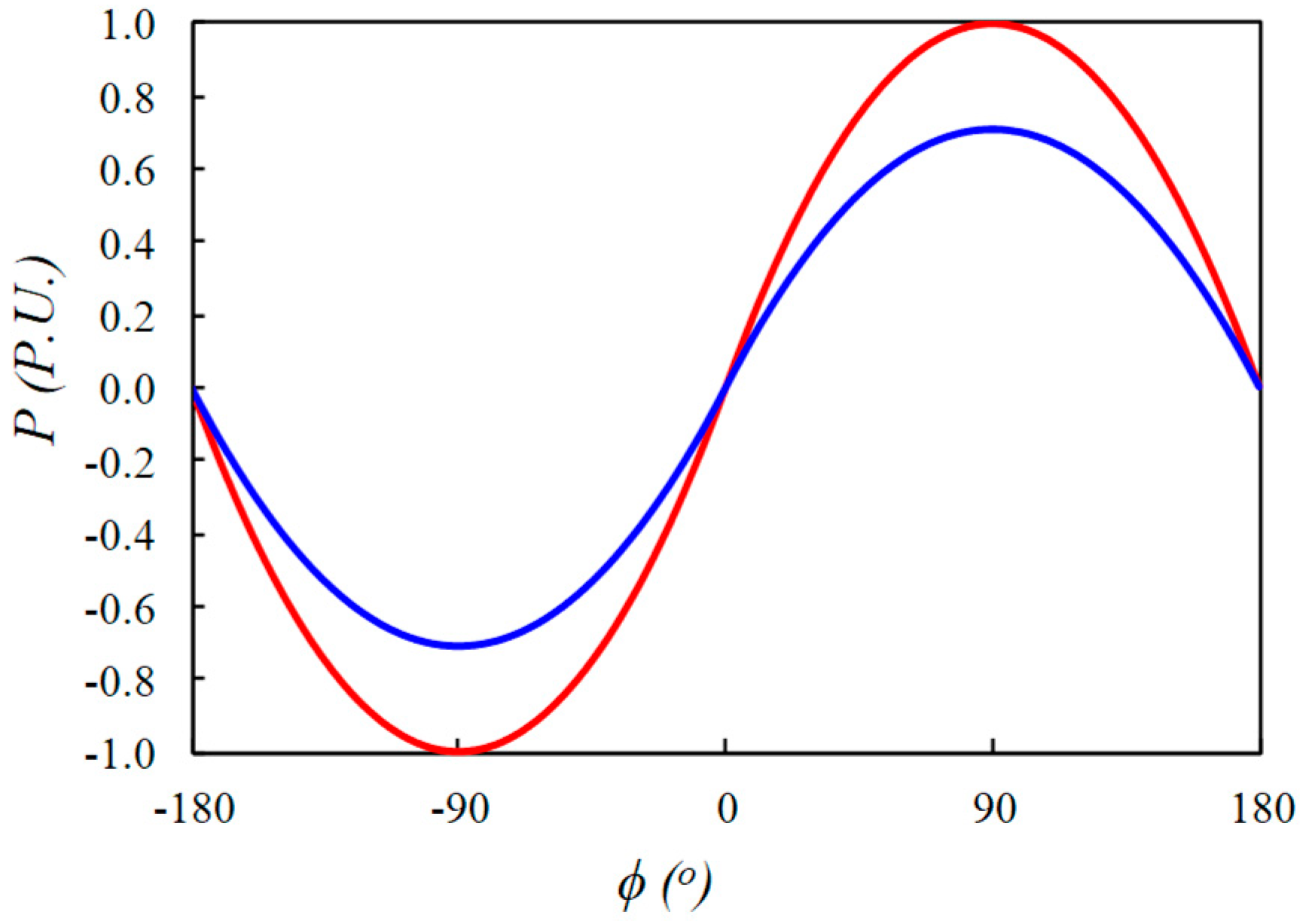
Figure 4 shows the evolution of the transferred power in units normalized to the maximum power value given in (10) as a function of the phase
ϕ for the minimum and maximum values of the voltage
V2 of the battery. The power transferred during the charging or discharging process at maximum output current (positive or negative) should remain between the two curves.
From (10), the equation that allows the design of the inductance
L can be obtained,
To improve the efficiency and reduce the EMI of the converter, it is necessary that the switching of the transistors be carried out in ZVS mode. This is only possible when (4) is positive, which determines a minimum value for the phase given by
therefore, the range where ZVS is possible is
Substituting (12) into (9), we got
then, the power range in ZVS mode is determined by
4. Analysis of the VF-IBDC
In the previous section, conditions were found to keep the primary (or secondary) bridge working in ZVS mode, and it is only possible to obtain ZCS switching for the
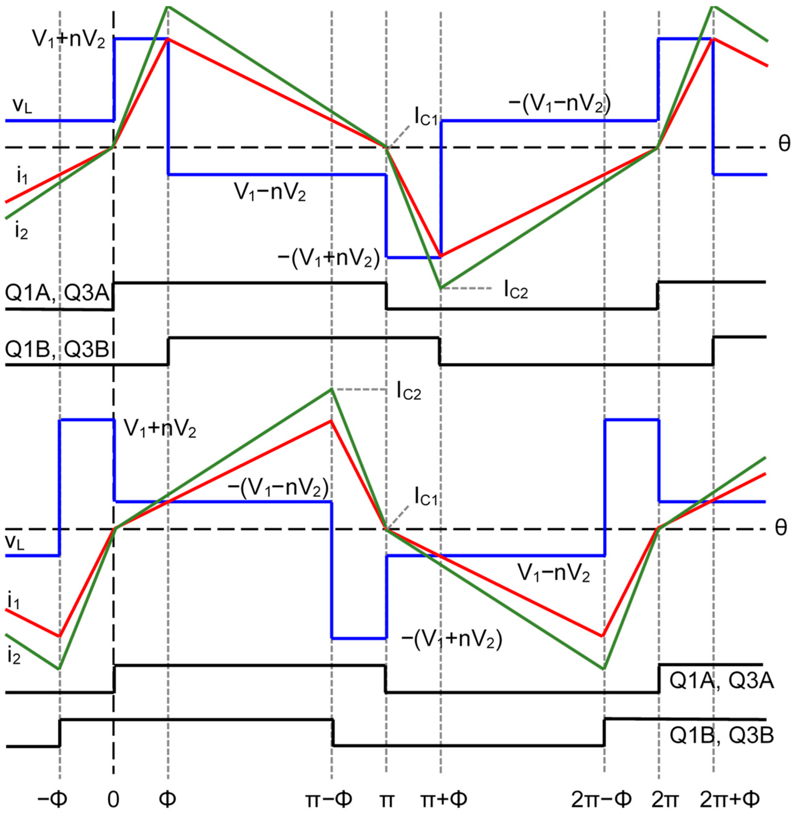
δmin phase where the waveforms become those shown in
Figure 5.
The signals in
Figure 5 are the same as those in
Figure 3, also showing the waveforms in charge mode (top) and discharge mode (bottom). Note that both turn-on and turn-off switching are carried out near the zero crossing of the current. This is an ideal situation where switching losses are minimal. To extend this condition with other power values, we should modify the switching frequency while maintaining the ZVS-ZCS condition with the appropriate adjustment of the phase so that δ meets (12). Therefore, the power is determined by (14) varying the phase shift and the switching frequency simultaneously. This is the concept of hybrid control that we present in the first section of this paper.
To carry out the converter design, the allowed frequency variation range must initially be set. Extending the frequency to very high values would increase the switching losses of the semiconductors and cause excessive conductor losses due to the skin effect, while frequencies that are too low would raise the flux density of the transformer and inductor core, increasing its losses or even causing magnetic saturation. In the present design, the allowed range goes from 100 kHz to 400 kHz for the highest possible range of transferred power.
If the output current
I2 is maintained at its maximum value for any value of battery voltage between
V2min and
V2max, the following design equation can be obtained to determine the value of the ratio transformer
n:
where
k = f1/
f2. Since (14) shows that power is inversely proportional to frequency, values for
f1 and
f2 are chosen in the lower part of the determined range. Given
f1 = 100 kHz and
f2 = 200 kHz,
n = 1.65 is obtained.
Now, (11) is not valid and the value of L is obtained by isolating it from (14),
Taking into account the values in
Table 1 and the value of
n in (16), a value of
L = 10.48 µH is obtained.
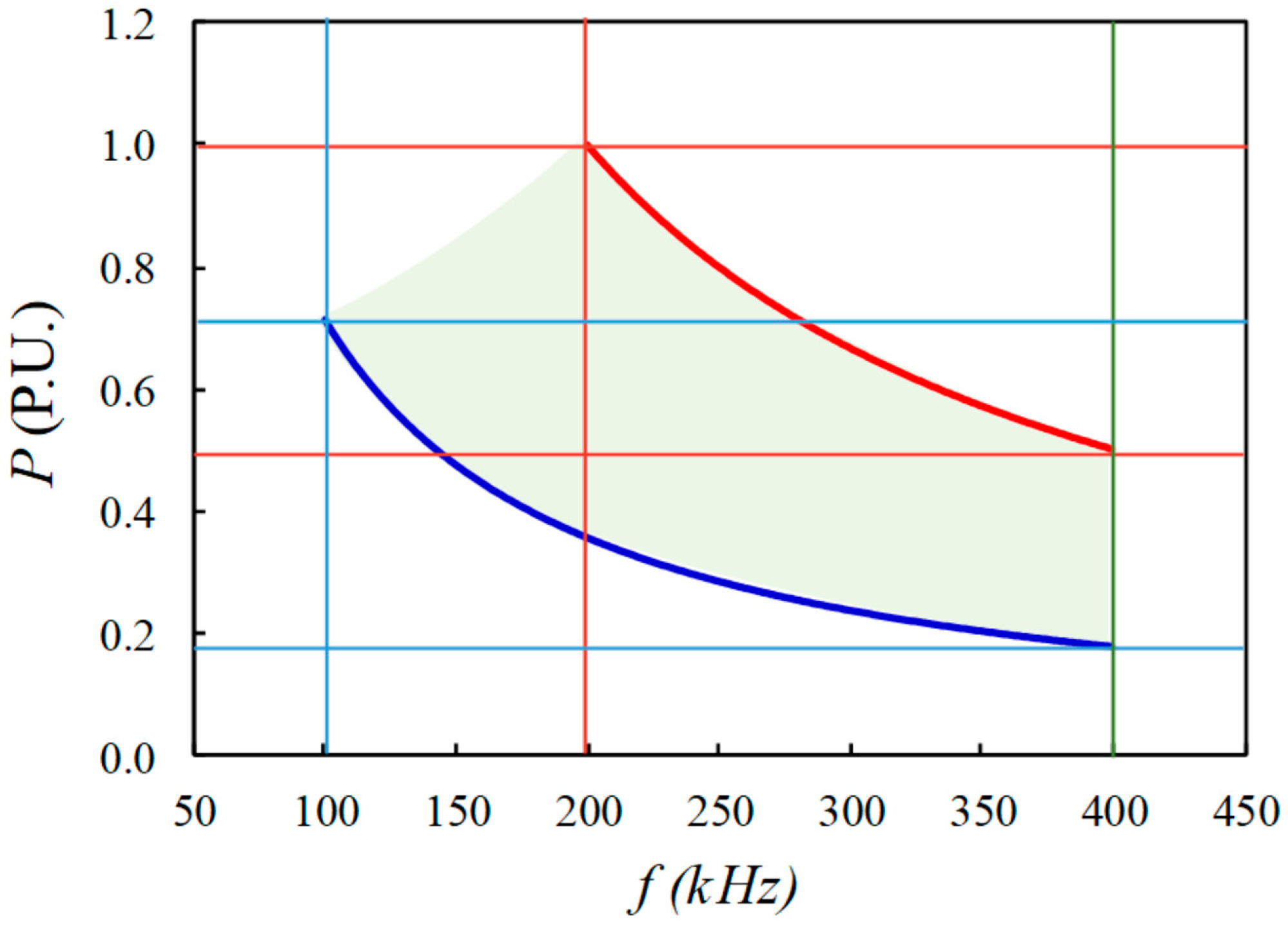
Figure 6 shows the evolution of the absolute value of transferred power in normalized units in function of the switching frequency for the minimum and maximum values of the voltage
V2 of the battery. The power transferred at maximum output current in ZVS and ZCS condition should remain between the two curves.
5. Comparative Analysis of Power Losses and Efficiency
A power loss analysis of the SPS-IBDC and VF-IBDC has been carried out considering the contribution of conduction and switching losses of the transistors, and the power losses of the core and the windings of the inductor and the transformer. In this study, residual losses in other non-active components (capacitors, cables, etc.) have not been considered. The analysis of
Psw focuses solely on the turn-off losses of the inverter bridge transistors as the turn-on switching losses are negligible due to the ZVS condition [
27].
In the practical implementation of the converter, the primary and secondary bridge switches have been configured differently. The primary bridge is made up of four switches with a single transistor; however, as the secondary bridge has more losses, each of its switches has two transistors in parallel. The transistor chosen is the SiC MOSFET C3M0016120K of VDS = 1200 V and RDson = 16 mΩ.
The losses in the diodes have been neglected since the conduction of the reverse current is also carried out through the transistor channel except during dead times. Thus, conduction losses for each transistor can be calculated only using (18).
where
PCD1 represents the conduction power losses of the primary bridge and
PCD2 represents the conduction power losses of secondary bridge.
The switching power losses of each transistor of the primary and secondary bridges can be calculated using the graphs of the turn-off switching energy
Eoff provided by the manufacturer using the following polynomial function.
where
a,
b and
c take the following values:
The switching turn-off losses of each transistor can be calculated with
On the other hand, the core losses of the inductor can be obtained using next equation:
where
PDI is the core loss density of the inductor given by the manufacturer for the operating frequency and magnetic flux density, and
VII is its volume. The inductor core is composed of two pieces of KOOL MU 6527 U core from Magnetics.
Analogously, the losses of the transformer core can be obtained by
where
PDT is the core loss density of the transformer, and
VTI is its volume. The transformer core is made with two pieces of the uncoated ferrite core U 126/91/20 from Magnetics. In both cases, the designs have been made with a flux density that guarantees non-saturation of the magnetic material. Specifically, the maximum flux density in the inductor core is 190 mT, and it is 100 mT in the transformer core.
In order to calculate the copper losses
PIC of the inductor, it is necessary to know the effective resistance of the winding
RI taking into account the conductivity, the total length and the skin effect using
For the two windings of the transformer, the power loss
PTC is given by
where
RT1 and
RT2 are the effective resistance of the primary and secondary transformer windings, respectively.
Therefore, the total power loss of the converter is
and the efficiency of the inverter can be calculated using
Table 2 shows the calculated results of the power loss analysis for the VF-IBDC converter specified in
Table 1 operating at maximum output current.
Figure 7 shows the evolution of the power losses and the efficiency of the VF-IBDC converter for different values of the output power expressed in normalized units referring to the value of the maximum output power. When the battery has its minimum voltage value (285 V), the loss and efficiency curves are shown in blue, while for the maximum voltage value (400 V), the curves are red. As the maximum charging current is the same in both cases (25 A), the maximum power obtained is reduced from 10,000 W to 7125 W when the battery voltage goes from 400 V to 285 V.
Table 3 shows the calculated results of the power loss analysis for the SPS-IBDC working in the same conditions maintaining the transformer configurations and changing the value of
L = 15.88 µH in order to obtain the maximum power determined in (11).
To complete the comparative loss analysis,
Figure 8 shows the power losses and efficiency of the SPS-IBDC converter versus output power.
Comparing
Table 2 and
Table 3, it is observed that the VF-IBDC presents an efficiency improvement of 6 percentage points at minimum battery voltage and maximum charging current. Looking at
Figure 7 and
Figure 8, a general improvement in efficiency is also observed at high output power values.
7. Experimental Results
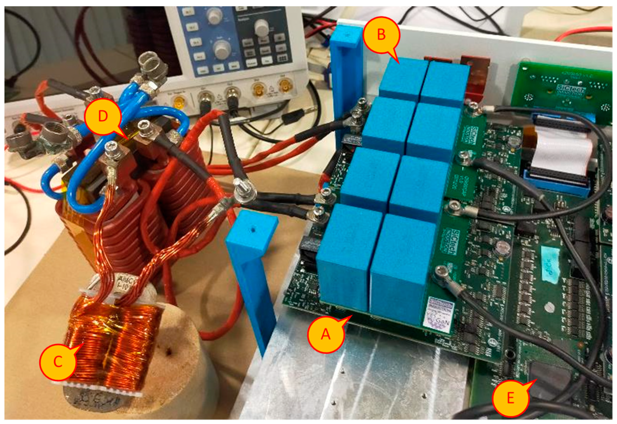
This section shows the experimental results obtained by testing a 10 kW VF-IBDC converter operating according to the specifications shown in
Table 1. The values of the components of the circuit are those obtained in previous sections. For the experimental verification, a test bed was constructed, consisting of the following elements:
- A.
A primary bridge with four C3M0016120K SiC MOSFETs mounted on a water cooling heatsink.
- B.
A secondary bridge with eight C3M0016120K SiC MOSFETs mounted on a water cooling heatsink.
- C.
An inductor L of 10.5 µH (including transformer leakage inductance).
- D.
A transformer T with n = 10:6.
- E.
An integrated digital electronic control on an FPGA-based system.
A and B are fully functional full bridge modules that include sensors, transistor trigger circuits and a power supply with galvanic isolation and high common-mode transient immunity (CMTI). V1 and V2 have been realized through IT6012C-800-50 bidirectional laboratory power supplies.
Figure 10 shows a picture of the test bed used to obtain the following experimental results.
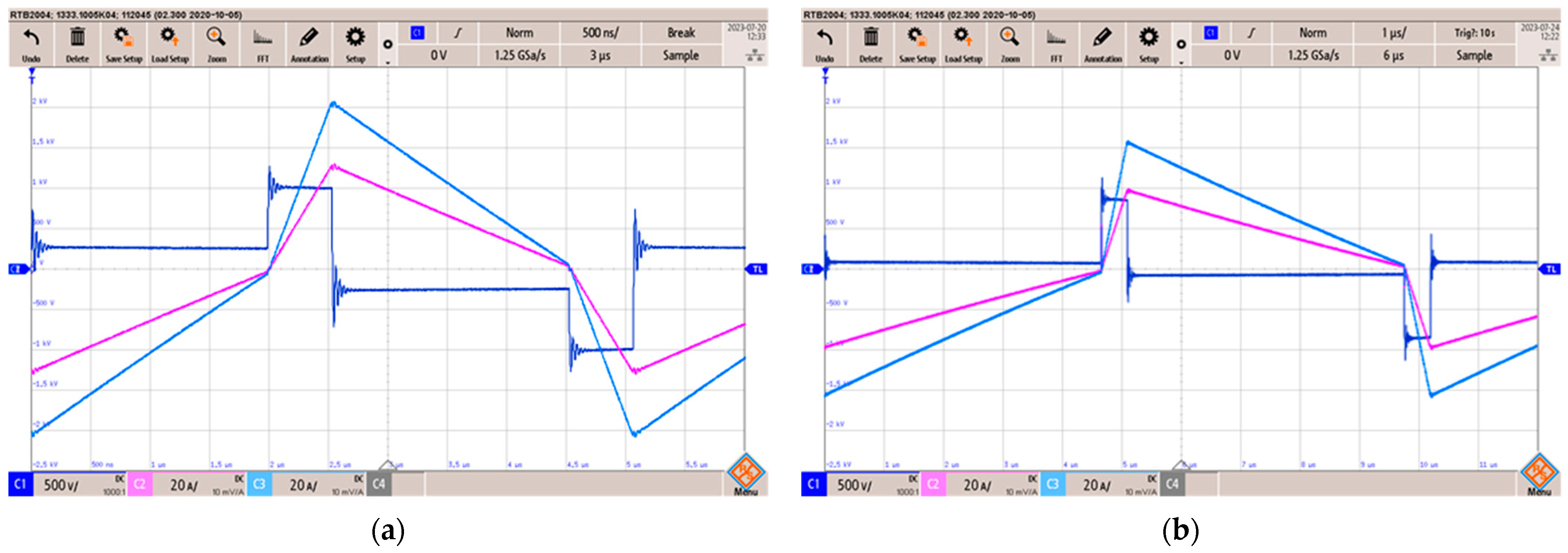
Figure 11 displays waveforms captured by a digital oscilloscope for the VF-IBDC converter operating at full power in charge mode with 385 V at the input. In
Figure 11a, the output voltage is 400 V, and in
Figure 11b, the output voltage is 285 V. In order to keep ZVS and quasi-ZCS conditions, the frequency changes from 197 kHz (
V2 = 400 V) to 98 kHz (
V2 = 285 V). The control circuit regulates the output current of 25 A constant in both cases.
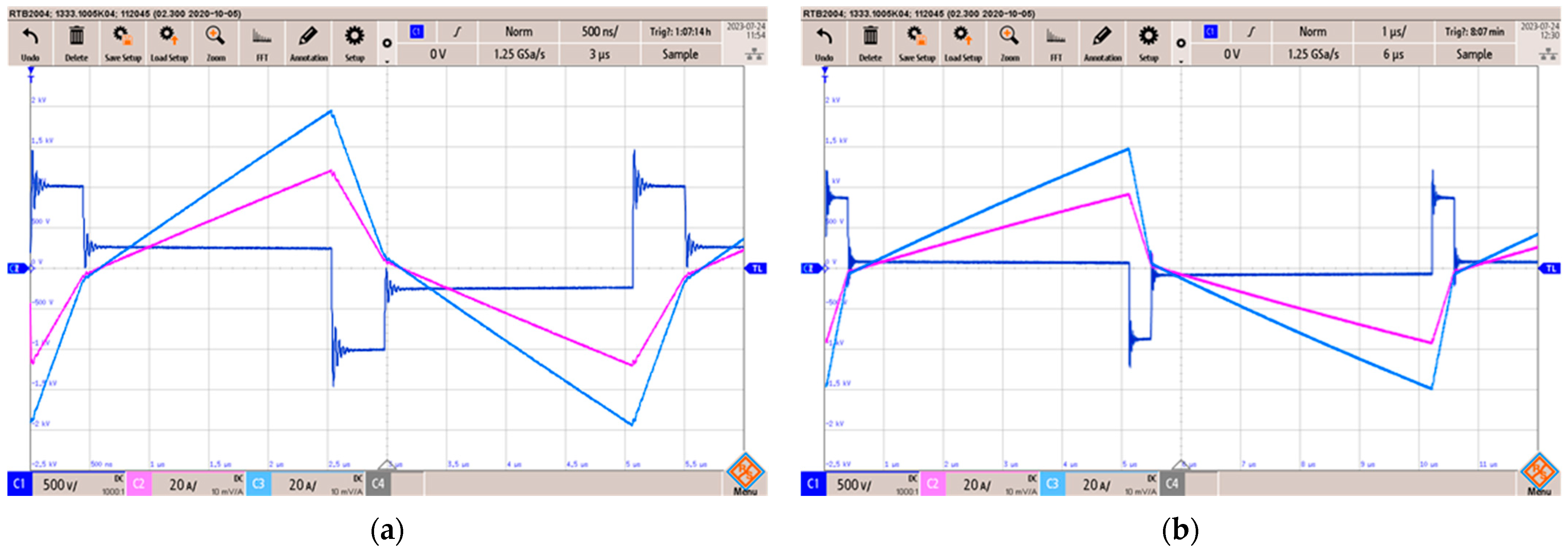
Figure 12 shows oscillograms in discharge mode when the power goes from
V2 = 400 V in
Figure 12a or
V2 = 285 V in
Figure 12b with
V1 = 385 V. Now, the regulated current
I2 is −25 A. The change of frequency in discharge mode is quite similar to that in charge mode.
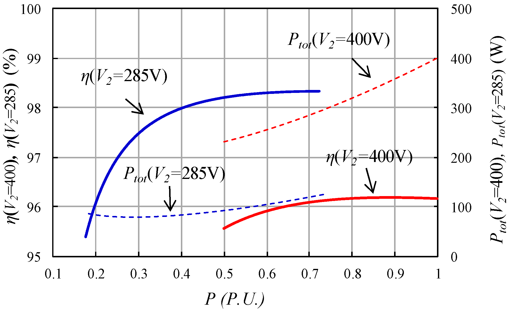
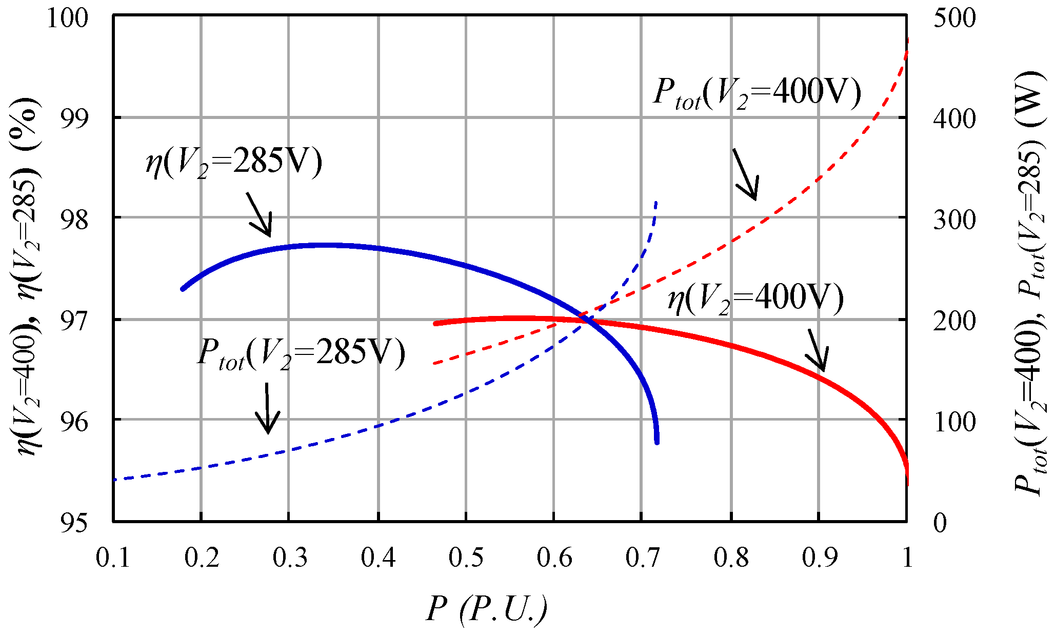
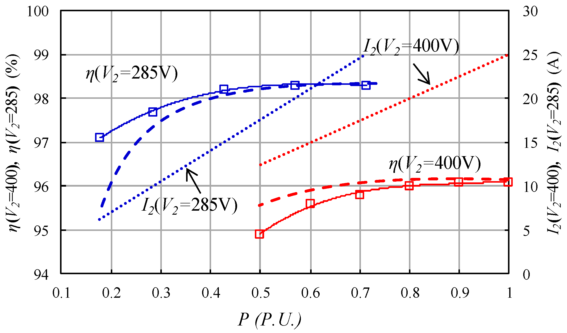
Finally,
Figure 13 shows the experimental measurements of the efficiency in charge mode regulating the output current until 25 A with
V1 = 385 V when
V2 is 400 V (red lines) and 285 V (blue lines). The results obtained in discharge mode were very similar. Note that there are some differences between the experimental and calculated results that may be due to the modeling method used, the existence of losses of other elements not taken into account in the calculation (capacitors, conductors, parasitic components, voltage and current sensors, etc.) and also the measurement process.
8. Discussion and Conclusions
This paper has carried out a complete study of the VF-IBDC converter that explores the combined effect of a variable frequency and a phase shift to control an isolated bidirectional dual active bridge DC–DC converter so that its primary bridge operates under ZVS and quasi-ZCS conditions over a wide operating range.
After an in-depth analysis of the operation of the SPS-IBDC, a complete design procedure has been presented that allows for the design of a VF-IBDC converter for a specific application of bidirectional charging of electric vehicle batteries.
To verify the viability of the design, a comparative analysis of power losses was developed that determined that the VF-IBDC converter is an enhanced solution that allows us to improve efficiency by up to 6 percentage points compared to the standard SPS method.
A fully functional control circuit has also been presented, easily implementable on the PSIM simulator, which allows us to check the correct operation of the converter and which was the basis of the control finally implemented on an FPGA-based system.
The feasibility of this design has been verified with the construction and testing of a 10 kW converter using SiC MOSFET transistors where an efficiency greater than 98% was achieved.


