Abstract
The co-integration of antennas with lighting sources appears as an effective way to distribute broadband networks closer to users, lowering interference and transmitted power, as well as to reduce energy consumption in future lighting systems. We here present an original contribution to the implementation of transparent and invisible antennas with OLED light sources. To validate the proposed approach, the honeycomb mesh technique was used, and an optical transparency of 75.4% was reached. The transparent mesh antenna was compared with the non-transparent full-metal antenna in terms of radio-electrical parameters. Our prototype was designed using copper films deposited on a glass substrate. The simulation results of the S-parameters and the radiation patterns were validated against measurements performed in an anechoic chamber. The directivity and gain obtained were dBi and dBi at , respectively. To study the effect of antenna integration with OLEDs, optical and photometric characterizations with and without the antenna were measured, and the colorimetric parameters were then treated using the IES TM-30-18 standard.
1. Introduction
Due to their excellent integration qualities, high energy efficiency, low luminance without glare, and potentially low manufacturing costs, Organic Light-Emitting Diodes (OLEDs) can be easily integrated into urban spaces for pedestrian lighting. Manufacturers are still reluctant to invest massively in this technology, despite its maturity, as long as the LED market is booming. Nevertheless, in recent years, OLEDs have rapidly progressed, and commercially available models are already used in internal and exterior lighting, displays, automotive applications, aerospace, wearable biomedical devices, etc. [1,2,3,4]. These developments are of great interest for manufacturers because it is obvious that this technology will be at the heart of the next generation of general lighting sources in smart cities [5]. Intelligence applications indeed require new wireless network infrastructures to support the increase in the volume of communication linked to new services. Furthermore, the installation of a connected network of smart city services needs a larger communication area. Therefore, it is necessary to install more antennas at the interfaces of all connected objects and to multiply the base stations in cities to achieve reliable communication [6]. Due to the miniaturization of these objects and the visual pollution caused by the installation of more base stations in cities, this requirement becomes difficult to fulfill [7]. For this reason, optically transparent antennas can be quite a promising solution to replacing non-transparent antennas. Because of their optical transparency, these antennas can be integrated into screens, glazing, bus stop indicators, OLED lamps, etc. More antennas means improvement in network coverage without increasing the visual or spatial impacts linked to their presence [8,9].
With the expansion of the transparent device market, optically transparent antennas have great potential for newer wireless communication systems. The manufacturing process is based on the deposition of electrically conductive and transparent material on transparent substrates [10,11]. According to the literature, the transparent materials used in the manufacture of these antennas are indium tin oxide (ITO) [12,13,14,15], fluorine-doped tin oxide (FTO) [16], aluminum-doped zinc oxide (AZO) [17], AgHT-4 [18,19], AgHT-8 [20,21,22,23]), ultra-thin metal film [24], and mesh structures [25,26,27,28,29,30,31].
The development of mobile devices benefits from the integration of antennas and transparent and flexible screen displays. The antenna-on-display (AoD) solution has already been implemented in the literature on OLED displays and Liquid Crystal Displays (LCDs). The original concept of optically invisible AoDs has been studied and tested in high-resolution OLED touch displays for WiFi and Bluetooth applications in smartwatches [32,33]. Furthermore, in [34], the authors presented a detailed study of an optically invisible antenna integrated into OLEDs and LCDs for smartphones. This antenna operates in the millimeter-wave (mm-Wave) band for 5G cellular applications. The techniques of diamond mesh and identical dummy grids are used to achieve optical invisibility and transparency. Dummy-grid structures are diamond-shaped and encompass the designed antenna region to eliminate any difference in optical transmittance. Similarly, Ref. [35] also presented an AoD that can eventually be integrated into display panels for the sub-6 band. In addition, a simulation study of optically transparent antennas that can be integrated into OLED light sources was presented in [7,36,37]. All these studies were carried out to understand the operation of an antenna integrated into OLEDs without taking into consideration the effect of this integration on the display’s color appearance.
This paper presents the design and realization of a transparent and invisible antenna, designed using a honeycomb mesh for the 5 WLAN band. This study focuses on two main challenges in order to examine the antenna integration effects on the OLED light source. The first is the transparent antenna design using the mesh technique. This analysis is based on a comparison between two antennas: a full-metal antenna and a honeycomb-meshed one. The honeycomb mesh technique is used to design the invisible and transparent antenna with high transparency and an acceptable sheet resistance value. The second one consists of antenna integration and its effects on the OLED panel’s visual characteristics. For this purpose, this paper aims to study the colorimetric parameters of a warm white OLED after the integration of the transparent mesh antenna. It contains a physical realization of the concepts analyzed in [37], which presented a comparative study on the simulation results of transparent circular patch antennas integrated into OLEDs. It is important to note that the meshing technique to achieve optical transparency has been widely discussed in the literature [7,25,26,27,28,29,30,31,32,33,34,35,36,37]. However, this paper presents, for the first time, a complete study, which contains the antenna electrical parameters and the colorimetric parameters of the OLED before and after antenna integration.
The remainder of this article is organized as follows: Section 2 describes the material characteristics used in the design. To justify the choice of the transparent antenna, Section 3 describes a comparison between this antenna and a non-transparent one. The experimental results are discussed and compared with the simulation results in Section 4. The method for antenna integration into an OLED light source and the effect of this integration on the radio-electrical parameters of the antenna and on the OLED colorimetric parameters are studied in Section 5. Conclusions and perspectives are presented in Section 6.
2. Material Characteristic
This article proposes the study of a transparent antenna integrated into an OLED light source to provide better connectivity for wireless communications. The proposed antenna is designed using transparent materials deposited on a glass substrate. Firstly, the characteristics of the materials used in this design are studied. These characteristics are the optical and dielectric parameters of the glass substrate and the sheet resistance and transparency of the ITO used in antenna manufacturing.
2.1. Substrate Characteristics
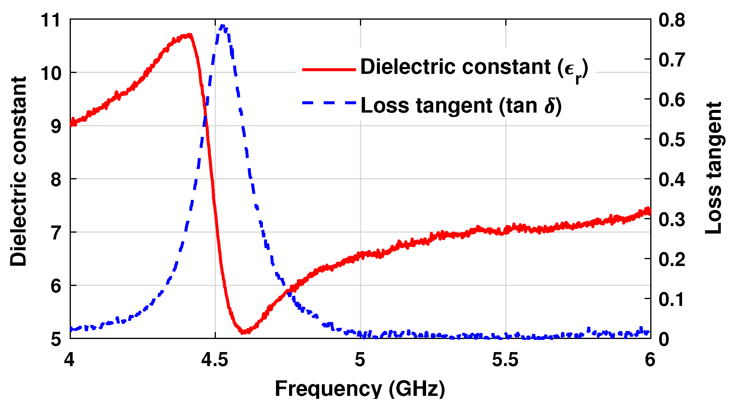
The main characteristics of interest are optical transparency (Tsub), dielectric permittivity (), and the tangent of the loss angle (). The dielectric parameters were measured using the Vector Network Analyzer combined with the 85,070 B dielectric probe kit with a tolerance of and on the dielectric permittivity and dielectric losses, respectively. The measurement results of and are shown in Figure 1. According to this figure, the measured values at a frequency of are and .
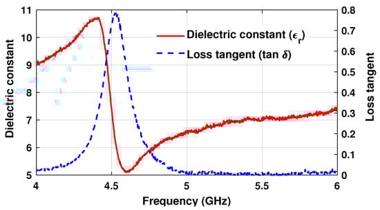
Figure 1.
Dielectric permittivity and tangent of the loss angle.
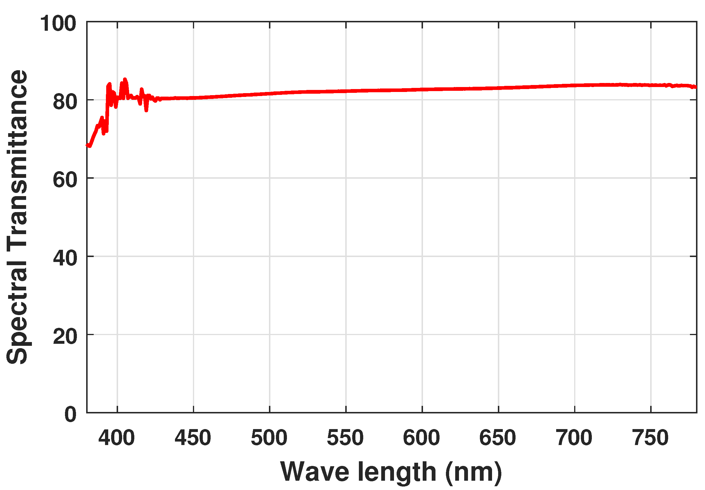
The other parameter studied is optical transparency in the visible spectrum. This parameter was measured using an optical bench at room temperature and a MINOLTA-CS-1000 spectroradiometer. First, the luminance of the OLED was measured. Secondly, the glass substrate was inserted through a lens holder in front of the objective, in order to intercept the entire luminance. Transparency is the ratio of the latter luminance to the first result at the corresponding wavelength. Figure 2 illustrates this optical transparency; the median value is around 82.5%. Noise below 480 results from low emission in this band, leading to an increased noise level.

Figure 2.
Optical transparency for glass substrate in the visible spectrum.
2.2. Sheet Resistance
The two popular types of transparent antennas are meshed and based on transparent conductive oxide (TCO)-type antennas. In this work, the ITO film and the mesh structure were studied and compared. The resistance of the sheet and the transparency T (%) were compared to identify the most-suitable material of this design.
2.2.1. ITO Film
One of the TCOs widely used in the design of transparent antennas is ITO films. OLEDs use ITO as an electrode for its conductive and transparent properties allowing light to go out. Several researchers also use this material in the manufacture of optically transparent antennas [12,14,15]. Its high optical transparency makes it an ideal candidate, but its high sheet resistance remains a challenge for the realization of antennas. The sheet resistance is the electrical resistance of a square surface of a material of thickness “t” [9]. The sheet resistance of the ITO film is given by the following relation:
where is the conductivity and “t” is the thickness of the ITO film.
2.2.2. Mesh Structure
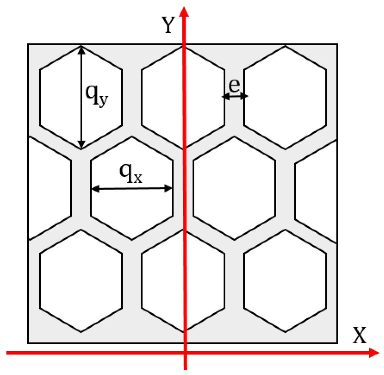
The structure of the metal mesh makes it possible to make optically transparent conductive films for antennas. The principle of the mesh technique is to create holes in a structure to let light pass. Transparency and sheet resistance change with the surface variation of these holes. Figure 3 represents the honeycomb structure chosen in this work. In general, the sheet resistance of the structure of the network is calculated by the equation [29]:
where is the sheet resistance of the copper film (calculated by Equation (1) with S/m and t = 370 nm), q is the pitch value, and e is the metal strip.
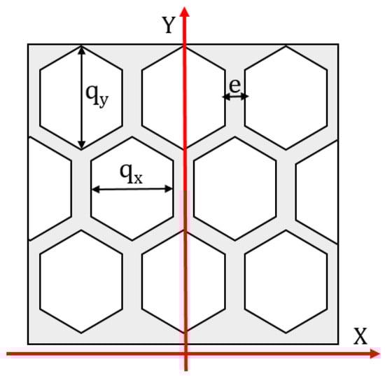
Figure 3.
The geometry of the honeycomb mesh.
Since the honeycomb structure was used, the leaf resistance was calculated in the and axes, compared to the direction of the current propagation in the meshed antenna. The resistors along each axis are given by the following relations:
The values of the chosen parameters are: , , , and (Equation (1)). Consequently, a value of approximately was obtained for the mesh. Note that this value is greater than the resistance of the copper film, but the use of these techniques increases the transparency of the material [25,29].
2.3. Optical Transparency
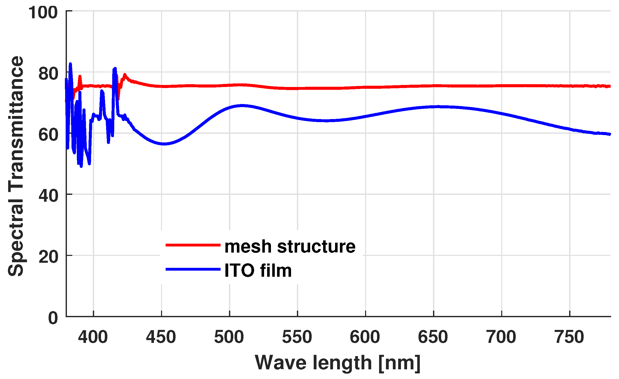
Optical transparency is another parameter that has been studied. Figure 4 illustrates a comparison between the optical transparency of the ITO film and the honeycomb structure from 380 to . Although large mesh dimensions are needed to obtain high optical transparency, this also increases sheet resistance. From this figure, the mesh structure has excellent transparency compared to the ITO throughout the entire visible spectrum. The measured transparencies remain constant. The median transparency value of the network structure is around 75.4%, while that of the ITO film is 65.1%. Note that the measured transparencies are the sum of the transparencies of two layers of the ITO and meshed structure deposited on the glass substrate.
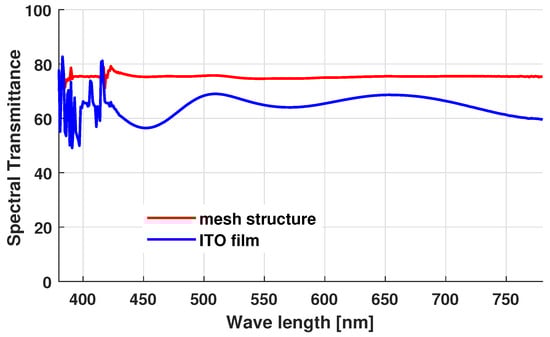
Figure 4.
Comparison between the optical transparency for the ITO film and mesh structure in the visible spectrum.
Global transparency results from the sum of three layers: two mesh grids and the substrate. Assuming that the contributions of the grids are identical, we can determine the contribution of the mesh as:
Inserting the previously measured transparency values in Equation (5), the transparency of the mesh can be evaluated as 95.5%. This suggests that if the OLED glass substrate and its anode can be used as the support and ground plane, respectively, the impact of a single mesh layer would be quite small. This argument goes in favor of the co-design and co-integration of the display and radiation functions.
2.4. Comparison between ITO and Mesh Technique
The comparison of the transparency and sheet resistance of the ITO film and mesh structure is given in Table 1. According to this table, the transparency of the mesh structure is 15.82% higher than that of the ITO film, while its sheet resistance is more than 20-times lower than that of the ITO. Therefore, the mesh structure obtains better performance compared to that of the ITO film. In this paper, the mesh structure was chosen to design the transparent antenna integrated into the OLED light source.

Table 1.
Comparisons between the ITO film and mesh structure.
2.5. Invisibility to the Bare Eye
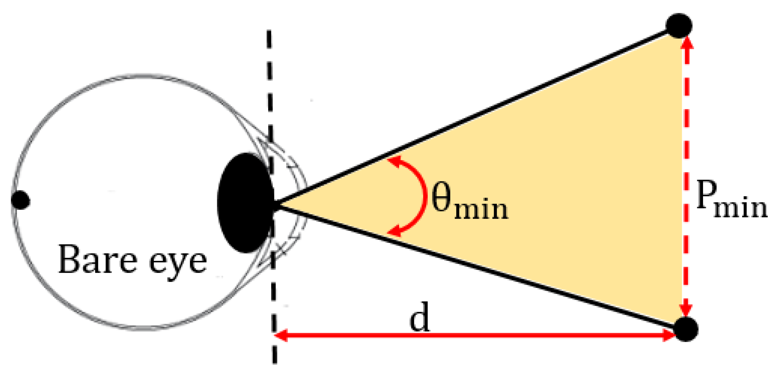
In order to integrate the mesh antenna into the OLED, the parameters of the honeycomb structure were optimized so that the human eye cannot distinguish the structure. The performance of the human eye was taken into account in this optimization. Therefore, the angular discrimination of the eye is [38]. The distance between two distinct points can be expressed as follows:
The distance d between the eye and the object depends on the intended application in which the mesh will be used (Figure 5). This distance is equal to the minimum value of the punctum proximum. Thus, a distance of was considered, which is quite sufficient for the antenna to be invisible in OLED light sources.

Figure 5.
Diagram of the discrimination of two points observed with the bare eye [38].
The distance calculated using Equation (6) is approximately . We can conclude that the mesh antenna using these parameters will be invisible to the bare eye at a minimum distance of .
3. Antenna Configurations
Two complementary case studies were implemented to investigate an antenna integrated into the OLED. The non-transparent antenna was designed with an all-copper film. The optically transparent and invisible antenna uses a honeycomb-shaped mesh structure. The all-metal version served as the reference standard for characterizing RF properties.
3.1. Non-Transparent Antennas
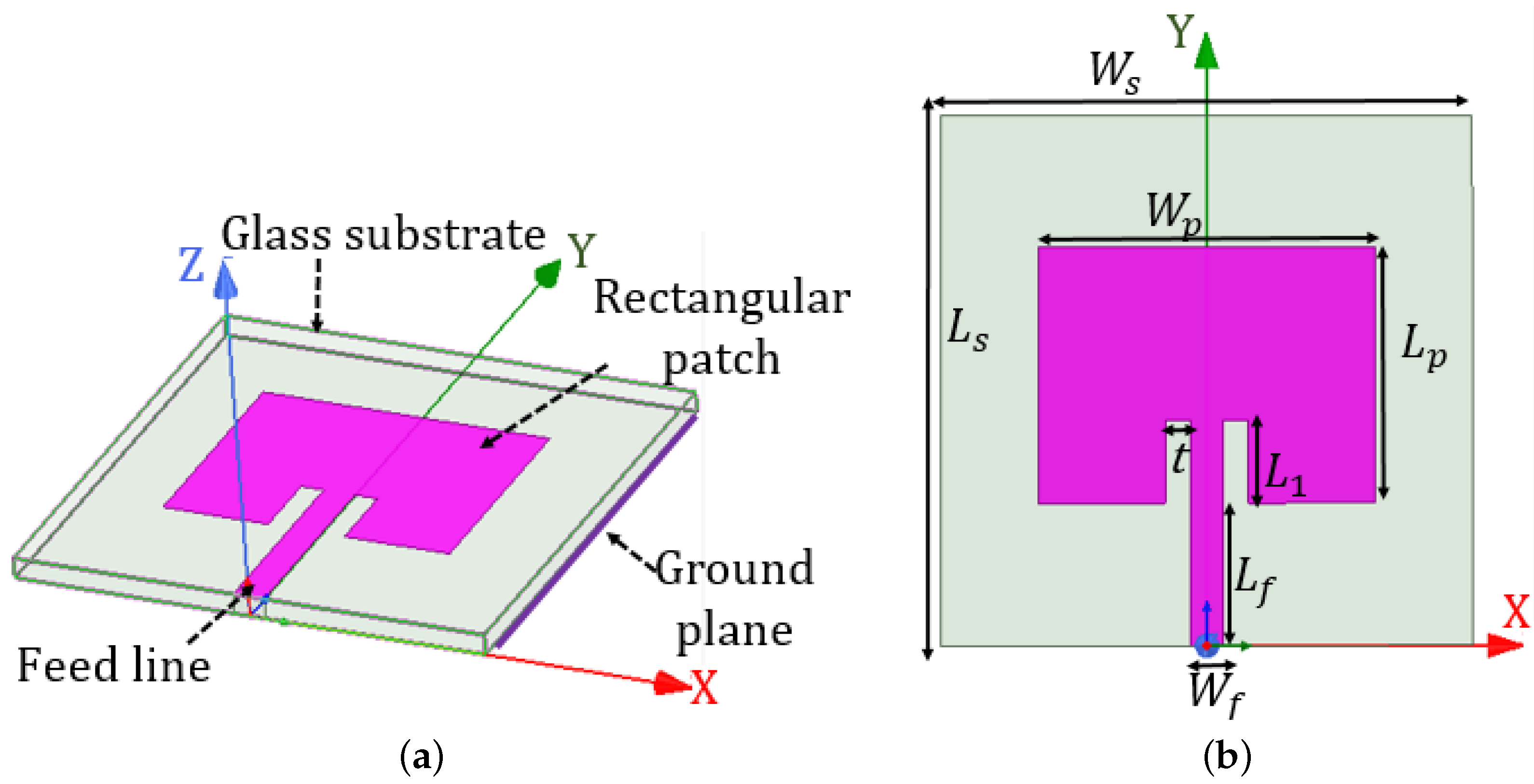
A reference non-transparent patch antenna was first designed using an entirely copper film. The geometry of the non-transparent antenna is shown in Figure 6. This antenna consists of a radiating element on one side of the glass substrate (thickness of ) and a ground plane on the other side.

Figure 6.
Rectangular patch antenna geometry: (a) 3D view, (b) top view. mm, mm, mm, mm, mm, mm, mm, and mm.
The width () and the length () of the antennas’ feedline were calculated to match the characteristic impedance of . Both antennas occupy a volume of . A copper film (conductivity of S/m, thickness of and sheet resistance of ) was used to design the two antennas. The dimensions were calculated using the equations in [39], so that the antenna operates in the WLAN band.
3.2. Transparent Antenna
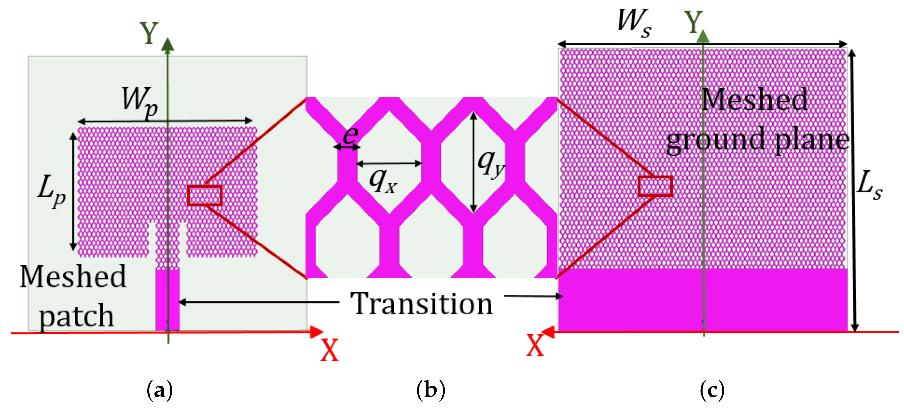
The transparent antenna designed using the honeycomb-shaped mesh structure can be integrated into an OLED light source structure with minimal impact on the luminous efficiency. The proposed antenna was designed to cover the WLAN band, but it can be operated on other bands by optimizing the mesh parameters. Figure 7 shows the geometry of the mesh antenna with the dimensions of the honeycomb mesh. For the ease of comparison, the non-transparent and mesh antennas have the same dimensions
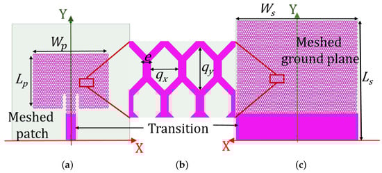
Figure 7.
Transparent antenna geometry: (a) meshed radiating patch, (b) mesh cells, and (c) meshed ground plane. and .
3.3. Comparison between the Non-Transparent and Transparent Antennas
Both designs were simulated and analyzed using an electromagnetic solver software, Ansys Electronics Desktop V.13.0.2. The electrical and radiation parameters of the antennas were compared. Figure 8 shows the comparison between the return losses for the compared antennas. For both candidates, the antenna impedance’s were well matched to at the resonance frequency of , because the return losses were less than dB. The bandwidth defined by ( dB) was 130 (– ) for the non-transparent antenna and 110 (– ) for the transparent antenna. It should be noted that the compared antennas had the same size; however, the disagreement observed between the resonance frequencies is justified by the resistance values for each structure (solid metal layer versus mesh metallic layer).
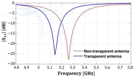
Figure 8.
Comparison between the return losses of the compared antennas (non-transparent and transparent).
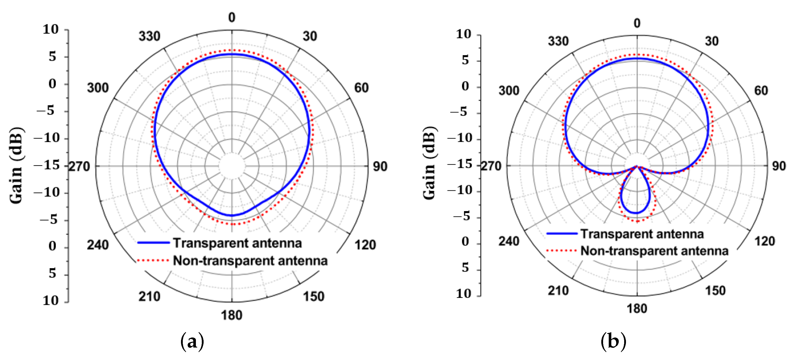
The radiation patterns for the two antennas are also compared in Figure 9. These diagrams are obtained for the resonance frequencies of each antenna and for the two planes: the XZ-plane (Figure 9a) and YZ-plane (Figure 9b). These results are in acceptable agreement because the antennas’ sizes are equivalent. The maximum gains were dBi and dBi for the non-transparent and transparent antennas, respectively. Both antennas achieved good gain in the operating band for WLAN applications. Therefore, increasing the resistance value of the sheet deteriorated the gain of the mesh antenna. This can be compensated by using meta-materials and applying array antenna techniques [40].
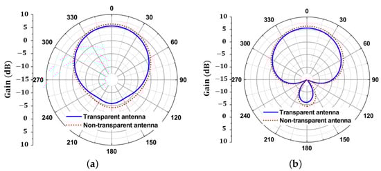
Figure 9.
Comparison between the radiation patterns of the compared antennas: (a) XZ-plane and (b) YZ-plane.
4. Experimental Results
The antennas were optimized using electromagnetic solver Ansys Electronics Desktop software and were manufactured by the photolithography process to validate the results obtained in the simulation. Figure 10a shows photographs of the fabricated antennas. Their reflection coefficients and radiation patterns were measured. The first was evaluated using the Vector Network Analyzer. The latter was measured inside an anechoic chamber, as shown in Figure 10b.
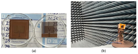
Figure 10.
Manufactured antennas: (a) non-transparent and transparent antennas; (b) antenna measurement chamber setup.
4.1. Reflection Coefficient Comparison
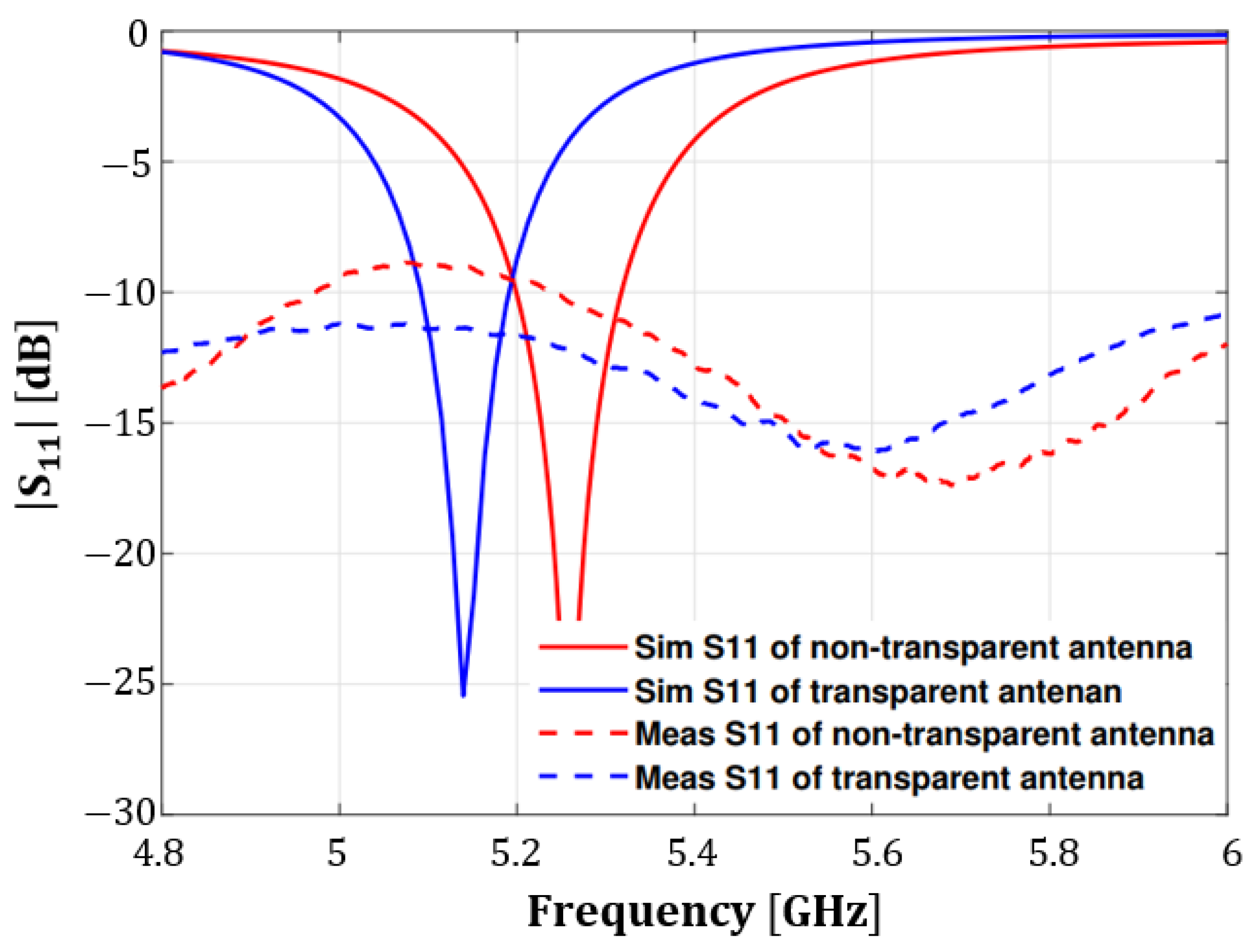
The simulated and measured reflection coefficient of the non-transparent and transparent antennas are shown in Figure 11. The impedance matching of the manufactured transparent antenna was not well matched; this may be justified among other things by the process inaccuracies in the manufacturing of the mesh antenna, the electrical losses of the glass substrate, and the increase in the resistance value of the sheet through the use of the mesh technique. Additionally, the metal thickness was so thin that it was comparable to the skin depth value of (calculated using the skin depth equation [24]); high loss was present, which reduced the performance of the antenna.
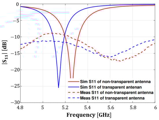
Figure 11.
Measured and simulated return loss of the transparent and non-transparent antennas.
To minimize the losses due to the skin depth, a metal thickness greater than should be used. However, the metal deposition technique used does not make it possible to obtain this thickness. However, the proposed antennas still exhibited acceptable impedance matching over the WLAN frequency band.
4.2. Radiation Patterns Comparison
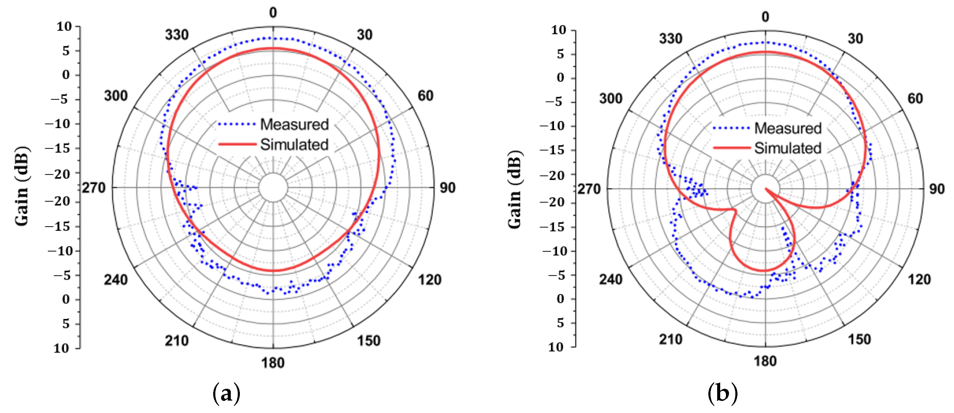
The far-field radiation patterns of the non-transparent antenna at are shown in Figure 12. Figure 13 shows the far-field radiation patterns of the transparent antenna at . In general, the simulated results matched the measured results. The observed deviations were attributed to the manufacturing problems and losses related to the electrical characteristics of the substrate. It was also observed that the antenna had an essentially unidirectional radiation pattern. The measured back radiation could not be evaluated due to the measurement configuration of the anechoic chamber.
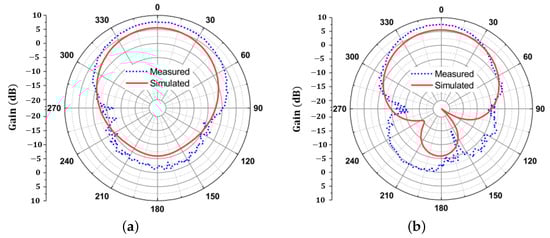
Figure 12.
Measured and simulated radiation patterns of the non-transparent antenna: (a) in the XZ-plane and (b) in the YZ-plane.
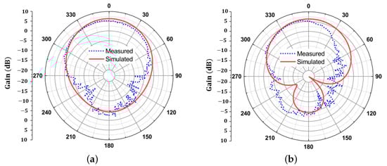
Figure 13.
Measured and simulated radiation patterns of the transparent mesh antenna: (a) in the XZ-plane and (b) in the YZ-plane.
5. Antenna Integration into OLED
OLEDs will become the most-suitable technology in future display and lighting systems, thanks to their many benefits, such as the high quality of light and images with excellent color rendering, low power consumption, controllability in terms of color temperature, and the possibility to realize them on transparent or flexible substrates with lower manufacturing costs. The integration of antennas in this technology can provide a solution in terms of the implementation of future lighting systems and the coverage area in wireless communication. In [34], the authors discussed the use of transparent antennas for future cities to improve network capacity, reduce visual pollution, and expand infrastructure in 5G wireless communication. These antennas will also be a good candidate for future 6G systems, in which all possible communication scenarios will be found, such as terrestrial wireless communication networks, satellite communication, intelligent transport, and the massive Internet of Things (IoT) [41]. Therefore, this work aimed to study the antennas’ integration into OLED technology to contribute to scientific research into the development of lighting systems. How to integrate a transparent antenna into OLED technology will be discussed in this section. The parameters of the OLED model used in this study are the same as those of the commercialized device [42].
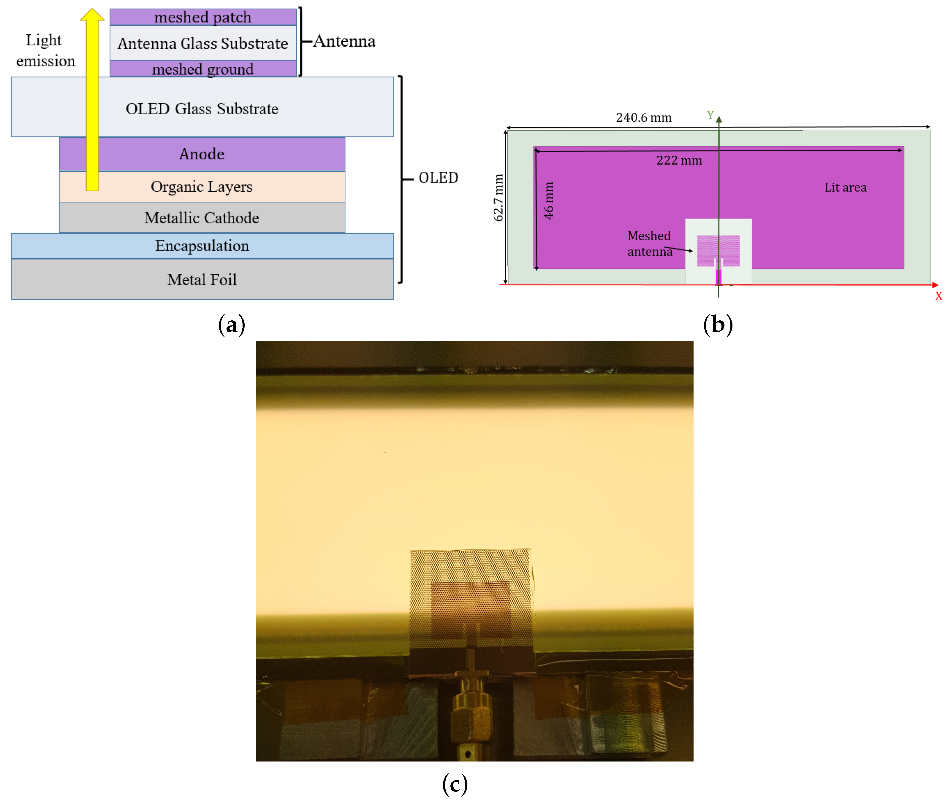
Generally speaking, an OLED is made up of several organic layers located between two electrodes. Each layer plays a specific role in the light-emission process. Figure 14 shows the OLED’s structure, including the antenna location. Figure 14a illustrates the different components of the OLED. Layer 1 is the -thick OLED glass substrate. To achieve proper OLED operation, the anode material must provide the balance between high transparency, good electrical conductivity, and good chemical stability. Additionally, the materials and thicknesses of the organic layers are crucial in the manufacturing of the OLED. The choice of materials and thicknesses of these layers, therefore, depends on the requirements and performance of the desired application. According to the literature, the most-used material is Alq3 (tris (8-hydroxyquinoline) aluminum) [43]. In the simulation model, Layer 2 is the ITO anode, whose thickness is 150 . Layer 3 contains the Hole Transport Layer (HTL), Electron Transport Layer (ETL), and Emissive Layer (EML) with a thickness of 270 . Layer 4 is the metal cathode made of aluminum and with a thickness of 120 . In order to protect the organic layers against oxidation, an encapsulation layer (Layer 5) is placed at the back of the cathode. After encapsulation, the metal Layer 6 is fixed for heat dissipation. Figure 14b shows the overall size of the proposed OLED model. The antenna is replaced on the front of the OLED to minimize the effect of the metal layer on its radiation, as shown in Figure 14c. The yellowish appearance is the result of the camera settings because the white balance was not set correctly.
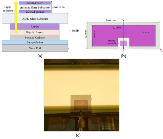
Figure 14.
Antenna integration into the OLED structure; (a) cross-sectional view, (b) top view, and (c) in the measurement step.
5.1. OLED Effects on the Antenna Performances
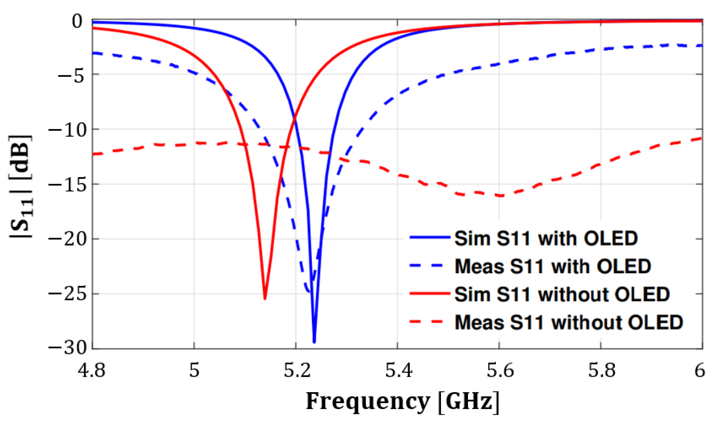
The comparison between the measured and simulated reflection coefficient of the antenna with and without the OLED is shown in Figure 15. From this figure, it can be observed that an acceptable agreement between the results was obtained and the bandwidth can well cover the desired WLAN frequency band. The transparent antenna return loss is affected by the OLED. The layers of the OLED also affect the antenna impedance, and it is less adapted at . The resonance frequency of the proposed antenna shifts to low frequencies with a narrow bandwidth.
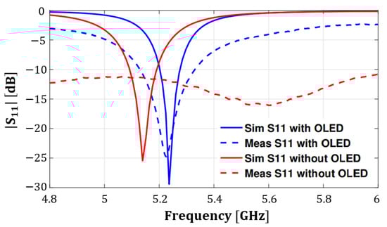
Figure 15.
Comparison between measured and simulated return loss and with/without OLED.
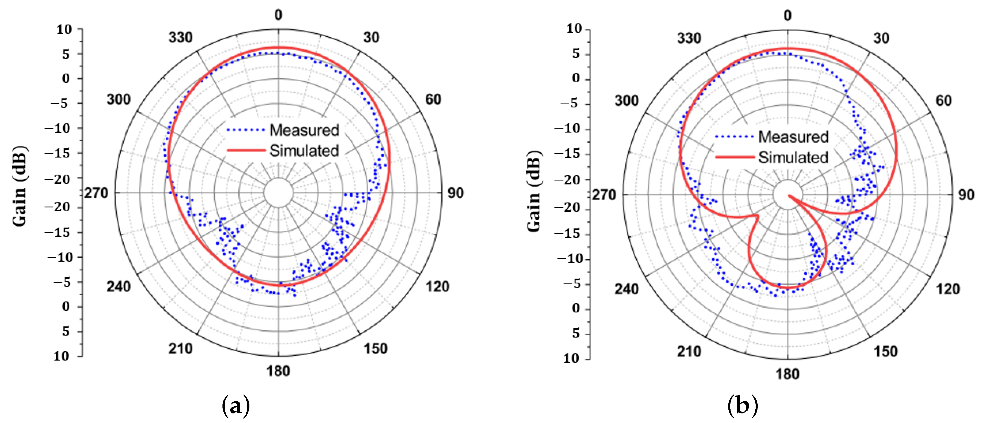
Figure 16 shows the comparison between the radiation patterns of the mesh antenna, with and without the OLED: Figure 16a in the XZ-plane, Figure 16b in the YZ-plane, and Figure 16c with the OLED in 3D view. These diagrams are oriented in the direction of the light emission from the OLED. The obtained directivity and gain of the antenna with the OLEDs are dBi and dBi, respectively, at . These values were improved after the integration of the OLED; this can be explained by the effect of the OLED layers, which are considered as the ground plane reflecting the antenna radiation.
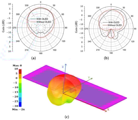
Figure 16.
Radiation patterns of the transparent antenna with and without OLED; (a) in the XZ-plane, (b) in the YZ-plane, and (c) with OLED in 3D view.
However, the materials used in the layers of the OLED light source are extremely critical for their efficiency and lifetime. The OLED panels contain ITO and aluminum electrodes and a metal foil layer, which serves as a reference ground for the antenna. The slight differences between the two results with and without the OLED can be interpreted by the effect of these layers on the antenna radiation. Since, the size of the layers is much larger than the size of the integrated antenna, these layers act as a large ground plane. This ground plane allows electromagnetic waves from the surface to be confined within the OLED panel, rather than radiating outwards. Therefore, these fields affect the electrical and radiation performance of the antenna.
5.2. Antenna Effects on the OLED Colorimetric Parameters
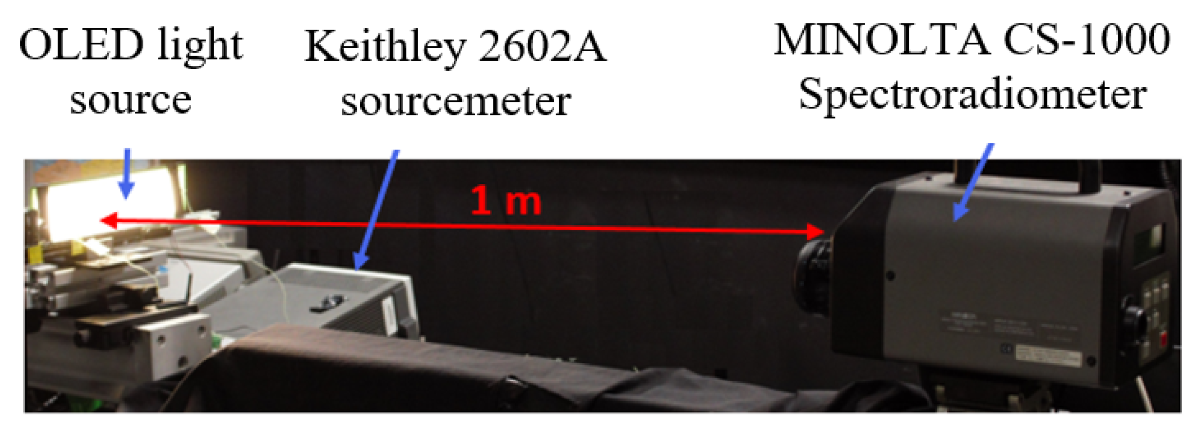
After the study of the effects of the OLED on the radio-electrical parameters of the antenna, it is very important to investigate the influence of this integration on the color appearance of the OLED. Therefore, the optical and photometric characterizations of the OLED were carried out before and after the antenna integration. Figure 17 shows a photograph of the optical and photonic measurements of the OLED. These measurements were carried out on an optical bench at room temperature with the MINOLTA CS-1000 spectroradiometer. This measuring device was placed 1 from the OLED, allowing the measurement of the optical and colorimetric parameters in the visible field (380–780 nm) in steps [44]. The measurements were carried out in both with and without the antenna and were repeated 21 times to ensure the accuracy of the measured values.

Figure 17.
Measuring bench for the optical characterizations.
Then, the colorimetric parameters were calculated using the IES TM-30-18 color-rendering method [45]. Using this method is more appropriate for LED and OLED light sources, because it generates bettercolorimetric analysis than the CIE fidelity index method. This involves calculating the mean fidelity index (Rf) by the light source rendering test from 99 Color Evaluation Samples (CES) compared to the International Commission on Illumination (CIE) standard [46], which only considers 8 Test Color Samples (TCS) to calculate Ra (Ra: color rendering index calculated according to the CIE 1995 CRI method). Colorimetric parameters such as the Spectral Power Distribution (SPD), Correlated Color Temperature (CCT), chromaticity coordinates (x,y) and (u′,v′), the Duv value (the distance between the chromaticity coordinates (u′,v′) of the OLED and the Planckian locus on the CIE 1976 color space), Rf (fidelity index), and Rg (Gamut index) were calculated to understand the change in the color appearance of the OLED after the integration of the antenna.
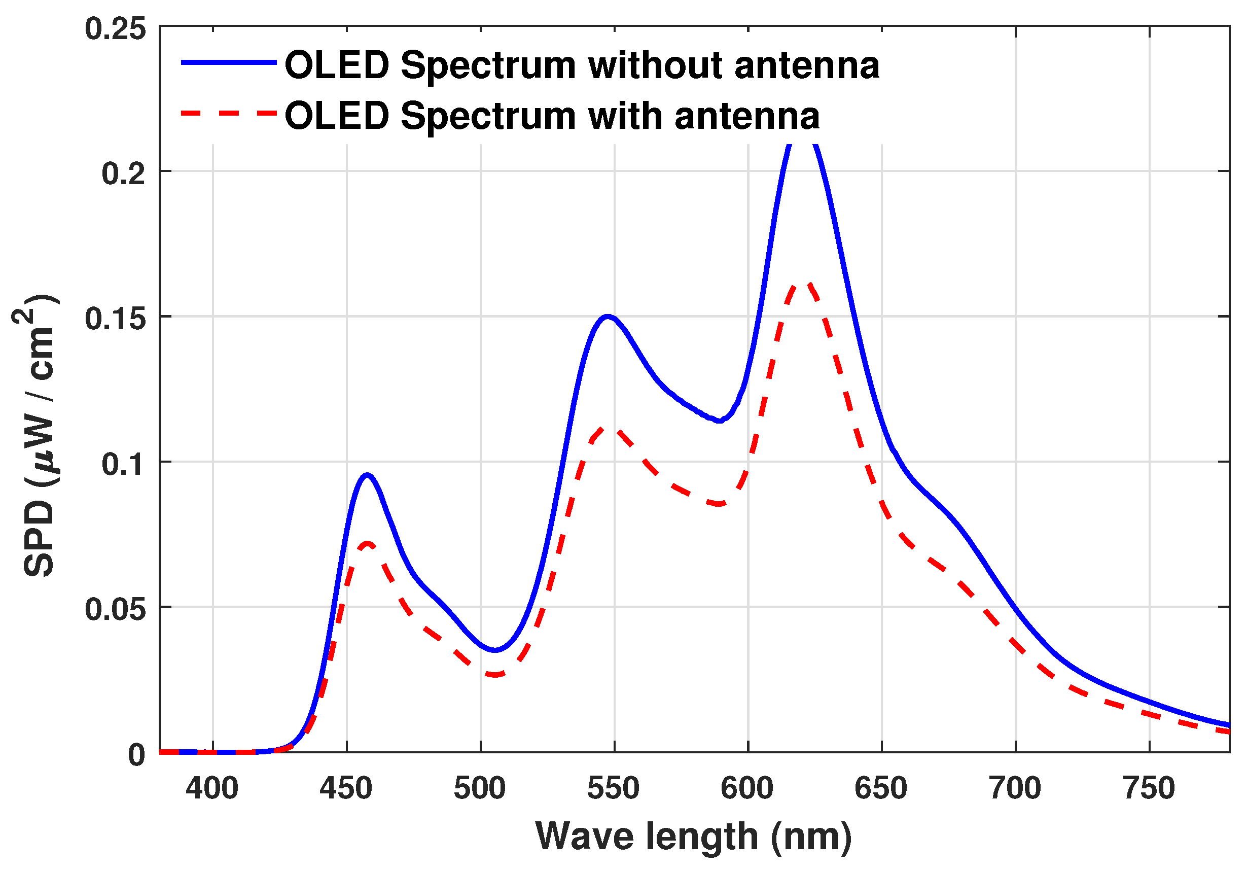
Figure 18 illustrates a comparison between the SPD of a warm white OLED (CCT = 3000 ) and the SPD of the OLED measured with the integrated antenna. It was noticed that the SPD changed after the integration of the antenna. A variation in the SPD generally results in changes in the colorimetric parameters.
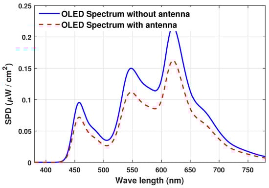
Figure 18.
The SPD of the OLED with and without the mesh transparent antenna.
The average CCT, chromaticity coordinates (x,y) and (u′,v′), Duv value, Rf, and Rg are shown in Table 2 for both the cases with and without the antenna. According to the MacAdam ellipse, the slight differences observed in these parameters are not detectable by users. The measurements, therefore, showed no significant difference between these parameters with and without the antenna. However, the luminance value decreased by 25% after the antenna was integrated, so this alteration will cause the lamp brightness to be non-uniform.
Table 2.
Measured colorimetric parameters of the OLED before and after antenna integration.
6. Conclusions and Perspectives
To the authors’ knowledge, this paper has proposed for the first time an original contribution with the experiment tests to integrate a transparent antenna into an OLED light source and can serve as a reference. The discussed method involved first designing a honeycomb mesh that achieved optical transparency. With the chosen mesh parameters, this transparency was approximately , while the antenna was not visible to the bare eye. This antenna was fabricated using a photolithography process and compared with its non-transparent counterpart in terms of the S-parameters and radiation patterns measured inside an anechoic chamber.
In addition, optical and photometric characterizations were carried out with and without an antenna. The luminance, spectral power distributions, correlated color temperature, CIE 1931 (x,y), CIE 1976 (u′,v′), Duv value, fidelity, and gamut indexes were calculated using the IES TM-30-18 color-rendering method. It was assessed that integrating the three-layer antenna degraded the luminance of the OLED by 25% due to the chosen substrate and mesh dimensions.
Optically transparent antennas will make it possible to replace conventional antennas in future devices. With the development of connected and intelligent objects, present in all sectors such as smart cities, smart lighting, transport, wearables, industry, smart hospitals, etc., these antennas will be crucial in future 6G applications. Therefore, future work will aim to improve the co-integration mechanism using some OLED layers as both a supporting and radiating element as an antenna. On the one hand, this will optimize the manufacturing cost by reducing the number of additional layers added. On the other hand, by minimizing the number of interfaces, it will reduce the transmission losses due to refractive index mismatches, thereby maximizing luminous efficiency. Furthermore, this approach to antenna/OLED co-integration could introduce new solutions for emerging technologies, such as transparent and flexible displays, wearable biomedical devices, and automotive lighting devices.
Author Contributions
Conceptualization, M.E.H. and L.C.; methodology, M.E.H.; software, M.E.H., P.D. and O.P.; validation, M.E.H., O.P., P.D. and L.C.; writing—original draft preparation, M.E.H., P.D. and L.C.; supervision, A.A., L.C. and G.Z.; writing—review and editing, A.A., G.Z. and L.C.; funding acquisition, L.C. All authors have read and agreed to the published version of the manuscript.
Funding
This work is supported by PHC Maghreb (Hubert Curien Program, grant number: 43981ZG) “MELINA” (Mastering Efficient Lighting in North Africa) supported by the French Ministry of Europe and Foreign Affairs and Campus France and, in Morocco, by the Ministry of Higher Education, Scientific Research and Innovation, in partnership with the National Center for Scientific and Technical Research (CNRST).
Data Availability Statement
The data will be provided upon request from the corresponding author.
Acknowledgments
The authors would like to express their sincere gratitude to Benoit Schlegel and Pierre Hernandez of the LAPLACE lab for their support in the antenna manufacturing.
Conflicts of Interest
The authors declare no conflicts of interest.
References
- Pode, R. Organic light emitting diode devices: An energy efficient solid state lighting for applications. Renew. Sustain. Energy Rev. 2020, 133, 110043. [Google Scholar] [CrossRef]
- Zissis, G.; Bertoldi, P.; Serrenho, T. Update on the Status of LED-Lighting World Market since 2018; Publications Office of the European Union: Luxembourg, 2021. [Google Scholar]
- Jeon, Y.; Noh, I.; Seo, Y.C.; Han, J.H.; Park, Y.; Cho, E.H.; Choi, K.C. Parallel-stacked flexible organic light-emitting diodes for wearable photodynamic therapeutics and color-tunable optoelectronics. ACS Nano 2020, 14, 15688–15699. [Google Scholar] [CrossRef] [PubMed]
- Jeon, Y.; Choi, H.R.; Lim, M.; Choi, S.; Kim, H.; Kwon, J.H.; Park, K.C.; Choi, K.C. A wearable photobiomodulation patch using a flexible red-wavelength OLED and its in vitro differential cell proliferation effects. Adv. Mater. Technol. 2020, 3, 1700391. [Google Scholar] [CrossRef]
- Zissis, G.; Dupuis, P.; Canale, L.; Pigenet, N. Smart lighting systems for smart cities. In Holistic Approach for Decision Making towards Designing Smart Cities; Springer: Berlin/Heidelberg, Germany, 2021; pp. 75–92. [Google Scholar]
- Green, R.B.; Guzman, M.; Izyumskaya, N.; Ullah, B.; Hia, S.; Pitchford, J.; Timsina, R.; Avrutin, V.; Ozgur, U.; Morkoc, H.; et al. Optically transparent antennas and filters: A smart city concept to alleviate infrastructure and network capacity challenges. IEEE Antennas Propag. Mag. 2019, 61, 37–47. [Google Scholar] [CrossRef]
- EL Halaoui, M.; Canale, L.; Asselman, A.; Zissis, G. An optically transparent antenna integrated in OLED light source for 5G applications. In Proceedings of the 2020 IEEE International Conference on Environment and Electrical Engineering and 2020 IEEE Industrial and Commercial Power Systems Europe (EEEIC/I&CPS Europe), Madrid, Spain, 9–12 June 2020. [Google Scholar]
- Park, J.; Park, D.; Kim, M.; Jung, D.; You, C.; Choi, D.; Lee, J.; Hong, W. Circuit-on-Display: A Flexible, Invisible Hybrid Electromagnetic Sensor Concept. IEEE J. Microwaves 2021, 1, 550–559. [Google Scholar] [CrossRef]
- Silva, Z.J.; Valenta, C.R.; Durgin, G. Optically transparent antennas: A survey of transparent microwave conductor performance and applications. IEEE Antennas Propag. Mag. 2020, 63, 27–39. [Google Scholar] [CrossRef]
- Lee, S.Y.; Choo, M.; Jung, S.; Hong, W. Optically transparent nanopatterned antennas: A review and future directions. Appl. Sci. 2018, 8, 901. [Google Scholar] [CrossRef]
- Sayem, A.S.M.; Lalbakhsh, A.; Esselle, K.P.; Esselle, J.L.; Buckley, B.; O’Flynn, B.; Simorangkir, R.B. Flexible transparent antennas: Advancements, challenges, and prospects. IEEE Open J. Antennas Propag. 2022, 3, 1109–1133. [Google Scholar] [CrossRef]
- Ali, N.M.; Misran, N.; Mansor, M.; Jamlos, M. Transparent solar antenna of 28 GHz using transparent conductive oxides (TCO) thin film. J. Phys. Conf. Ser. 2017, 852, 012036. [Google Scholar]
- Cai, L. An on-glass optically transparent monopole antenna with ultrawide bandwidth for solar energy harvesting. Electronics 2019, 8, 916. [Google Scholar] [CrossRef]
- Potti, D.; Tusharika, Y.; Alsath, M.G.N.; Kirubaveni, S.; Kanagasabai, M.; Sankararajan, R.; Narendhiran, S.; Bhargav, P.B. A novel optically transparent UWB antenna for automotive MIMO communications. IEEE Trans. Antennas Propag. 2021, 69, 3821–3828. [Google Scholar] [CrossRef]
- Lai, S.; Wu, Y.; Zhu, X.; Gu, W.; Wu, W. An optically transparent ultrabroadband microwave absorber. IEEE Photonics J. 2017, 9, 5503310. [Google Scholar] [CrossRef]
- Thampy, A.S.; Dhamodharan, S.K. Performance analysis and comparison of ITO-and FTO-based optically transparent terahertz U-shaped patch antennas. Phys.-Low-Dimens. Syst. Nanostruct. 2015, 66, 52–58. [Google Scholar] [CrossRef]
- Wu, C.T.; Ho, Y.R.; Huang, D.Z.; Huang, J.J. AZO/silver nanowire stacked films deposited by RF magnetron sputtering for transparent antenna. Surf. Coat. Technol. 2020, 360, 95–102. [Google Scholar] [CrossRef]
- Song, H.J.; Hsu, T.Y.; Sievenpiper, D.F.; Hsu, H.P.; Schaffner, J.; Yasan, E. A method for improving the efficiency of transparent film antennas. IEEE Antennas Wirel. Propag. Lett. 2020, 7, 753–756. [Google Scholar] [CrossRef]
- Azini, A.S.; Kamarudin, M.R.; Rahman, T.B.A.; Iddi, H.U.; Abdulrahman, A.Y.; Jamlos, M.F. Transparent antenna design for WiMAX application. Prog. Electromagn. Res. 2013, 138, 133–141. [Google Scholar] [CrossRef]
- Desai, A.; Upadhyaya, T.; Palandoken, M.; Gocen, C. Dual band transparent antenna for wireless MIMO system applications. Microw. Opt. Technol. Lett. 2019, 61, 1845–1856. [Google Scholar] [CrossRef]
- Desai, A.; Upadhyaya, T.; Patel, R. Compact wideband transparent antenna for 5G communication systems. Microw. Opt. Technol. Lett. 2019, 61, 781–786. [Google Scholar] [CrossRef]
- Desai, A.; Palandoken, M.; Elfergani, I.; Akdag, I.; Zebiri, C.; Bastos, J.; Rodriguez, J.; Abd-Alhameed, R.A. Transparent 2-element 5G MIMO antenna for sub-6 GHz applications. Electronics 2022, 11, 251. [Google Scholar] [CrossRef]
- Yasin, T.; Baktur, R.; Furse, C. A comparative study on two types of transparent patch antennas. In Proceedings of the 2011 XXXth URSI General Assembly and Scientific Symposium, Istanbul, Turkey, 13–20 August 2011; pp. 1–4. [Google Scholar]
- Martin, A.; Gautier, C.; Castel, X.; Himdi, M. Transparent and miniature FM antenna in printed technology. Int. J. Microw. Wirel. Technol. 2018, 10, 19–24. [Google Scholar] [CrossRef]
- Hautcoeur, J.; Castel, X.; Colombel, F.; Benzerga, R.; Himdi, M.; Legeay, G.; Motta-Cruz, E. Transparency and electrical properties of meshed metal films. Thin Solid Film. 2011, 519, 3851–3858. [Google Scholar] [CrossRef]
- Dao, Q.H.; Grundmann, L.; Geck, B. Optically Transparent 24 GHz Analog Front-End Based on Meshed Microstrip Lines for the Integration in a Self-Sufficient RFID Sensor Tag. IEEE J. Radio Freq. Identif. 2019, 4, 83–92. [Google Scholar] [CrossRef]
- Yu, P.C.; Hong, C.C.; Liou, T.M. Bendable transparent conductive meshes based on multi-layer inkjet-printed silver patterns. J. Micromechan. Microeng. 2016, 26, 035012. [Google Scholar] [CrossRef]
- Kang, S.H.; Jung, C.W. Transparent patch antenna using metal mesh. IEEE Trans. Antennas Propag. 2018, 66, 2095–2100. [Google Scholar] [CrossRef]
- Martin, A.; Castel, X.; Himdi, M.; Lafond, O. Mesh parameters influence on transparent and active antennas performance at microwaves. AIP Adv. 2011, 7, 085120. [Google Scholar] [CrossRef]
- Zhang, Y.; Shen, S.; Chiu, C.Y.; Murch, R. Hybrid RF-solar energy harvesting systems utilizing transparent multiport micromeshed antennas. IEEE Trans. Microw. Theory Tech. 2019, 67, 4534–4546. [Google Scholar] [CrossRef]
- Hautcoeur, J.; Colombel, F.; Castel, X.; Himdi, M.; Cruz, E.M. Radiofrequency performances of transparent ultra-wideband antennas. Prog. Electromagn. Res. 2011, 22, 259–271. [Google Scholar] [CrossRef]
- Hong, W.; Lim, S.; Ko, S.; Kim, Y.G. Optically invisible antenna integrated within an OLED touch display panel for IoT applications. IEEE Trans. Antennas Propag. 2017, 65, 3750–3755. [Google Scholar] [CrossRef]
- Hong, W.; Ko, S.; Kim, Y.G.; Lim, S. Invisible antennas using mesoscale conductive polymer wires embedded within OLED displays. In Proceedings of the 2017 11th European Conference on Antennas and Propagation (EUCAP), Paris, France, 19–24 March 2017. [Google Scholar]
- Park, J.; Lee, S.Y.; Kim, J.; Park, D.; Choi, W.; Hong, W. An optically invisible antenna-on-display concept for millimeter-wave 5G cellular devices. IEEE Trans. Antennas Propag. 2019, 67, 2942–2952. [Google Scholar] [CrossRef]
- Kim, M.; Lee, D.; Oh, Y.; Lee, J.Y.; Kim, B.; Park, J.; Park, D.; Hong, W. Antenna-on-display concept on an extremely thin substrate for sub-6 GHz wireless applications. IEEE Trans. Antennas Propag. 2022, 70, 5929–5934. [Google Scholar] [CrossRef]
- El Halaoui, M.; Canale, L.; Asselman, A.; Zissis, G. Design and Analysis of Transparent and Non-Transparent Antennas Integrated in OLED at 3.5 GHz Band for 5G Applications. In Proceedings of the 2021 IEEE International Conference on Environment and Electrical Engineering and 2021 IEEE Industrial and Commercial Power Systems Europe (EEEIC/I&CPS Europe), Bari, Italy, 7–10 September 2021. [Google Scholar]
- El Halaoui, M.; Canale, L.; Dupuis, P.; Asselman, A.; Zissis, G. An Optically Transparent Mesh-Antenna Integrated in OLEDs for WLAN Applications. In Proceedings of the 2021 IEEE Industry Applications Society Annual Meeting (IAS), Vancouver, BC, Canada, 10–14 October 2021. [Google Scholar]
- Charman, W.N. Static accommodation and the minimum angle of resolution. Am. J. Optom. Physiol. Opt. 1986, 63, 915–921. [Google Scholar] [CrossRef]
- Balanis, C.A. Antenna Theory: Analysis and Design, 4th ed.; John Wiley & Sons: Hoboken, NJ, USA, 2016. [Google Scholar]
- Kaabal, A.; El Halaoui, M.; Amhaimar, L.; Azizi, S.; Dellaoui, S.; Ahyoud, S.; Asselman, A. Array antenna design with dual resonators 1D-EBG for enhancement of directivity and radiation bandwidth. Int. J. Microw. Opt. Technol. 2019, 14, 231–239. [Google Scholar]
- Ikram, M.; Sultan, K.; Lateef, M.F.; Alqadami, A.S. A road towards 6G communication—A review of 5G antennas, arrays, and wearable devices. Electronics 2022, 11, 169. [Google Scholar] [CrossRef]
- OLED-Works. Lumiblade OLED Panel Brite FL300. Available online: https://www.oledworks.com/wp-content/uploads/2016/03/Data-sheet-Lumiblade-OLED-Panel-Brite-FL300L-ww-wm-1.pdf (accessed on 20 November 2023).
- Muhammad, F.F.; Hapip, A.I.A.; Sulaiman, K. Study of optoelectronic energy bands and molecular energy levels of tris (8-hydroxyquinolinate) gallium and aluminum organometallic materials from their spectroscopic and electrochemical analysis. J. Organomet. Chem. 2010, 695, 2526–2531. [Google Scholar] [CrossRef]
- Nilsson, T.H. Photometric specification of images. J. Mod. Opt. 2009, 56, 1523–1535. [Google Scholar] [CrossRef]
- Abdellah, O.B.; Al Haddad, A.; El Halaoui, M.; Dupuis, P.; Canale, L.; Asselman, A.; Zissis, G. Colorimetric Characterizations of Large Area White OLEDs Under Thermal and Electrical Stress Using TM-30-18 Method. In Proceedings of the 2020 Fifth Junior Conference on Lighting (Lighting), Ruse, Bulgaria, 24–26 September 2020. [Google Scholar]
- International Commission on Illumination: Method of Measuring and Specifying Colour Rendering Properties of Light Sources: Technical Report: CIE 013.3-1995. Available online: https://cie.co.at/publications/method-measuring-and-specifying-colour-rendering-properties-light-sources (accessed on 22 November 2023).


Disclaimer/Publisher’s Note: The statements, opinions and data contained in all publications are solely those of the individual author(s) and contributor(s) and not of MDPI and/or the editor(s). MDPI and/or the editor(s) disclaim responsibility for any injury to people or property resulting from any ideas, methods, instructions or products referred to in the content. |
© 2024 by the authors. Licensee MDPI, Basel, Switzerland. This article is an open access article distributed under the terms and conditions of the Creative Commons Attribution (CC BY) license (https://creativecommons.org/licenses/by/4.0/).