Article

A High-Performance and Ultra-Low-Power Accelerator Design for Advanced Deep Learning Algorithms on an FPGA

by
Achyuth Gundrapally
*,†,
Yatrik Ashish Shah
*,†,
Nader Alnatsheh
and
Kyuwon Ken Choi
DA-Lab, Department of Electrical and Computer Engineering, Illinois Institute of Technology, 3301 South Dearborn Street, Chicago, IL 60616, USA
*
Authors to whom correspondence should be addressed.
These authors contributed equally to this work.
Electronics 2024, 13(13), 2676; https://doi.org/10.3390/electronics13132676
Submission received: 28 May 2024 / Revised: 30 June 2024 / Accepted: 5 July 2024 / Published: 8 July 2024
(This article belongs to the Section Microelectronics)

Abstract

This article addresses the growing need in resource-constrained edge computing scenarios for energy-efficient convolutional neural network (CNN) accelerators on mobile Field-Programmable Gate Array (FPGA) systems. In particular, we concentrate on register transfer level (RTL) design flow optimization to improve programming speed and power efficiency. We present a re-configurable accelerator design optimized for CNN-based object-detection applications, especially suitable for mobile FPGA platforms like the Xilinx PYNQ-Z2. By not only optimizing the MAC module using Enhanced clock gating (ECG), the accelerator can also use low-power techniques such as Local explicit clock gating (LECG) and Local explicit clock enable (LECE) in memory modules to efficiently minimize data access and memory utilization. The evaluation using ResNet-20 trained on the CIFAR-10 dataset demonstrated significant improvements in power efficiency consumption (up to 22%) and performance. The findings highlight the importance of using different optimization techniques across multiple hardware modules to achieve better results in real-world applications.

1. Introduction

Field Programmable Gate Array (FPGA) applications, personal mobile devices, autonomous vehicles, surveillance and security, healthcare, and robotics all utilize convolutional neural networks (CNNs) for object-detection applications [1]. Convolutional neural networks (CNNs) are critical for many object-detection systems, whether deployed on cloud-based platforms or edge devices, due to their high recognition accuracy [2,3]. However, implementing CNN applications poses significant challenges because they require substantial power and computational resources to achieve high accuracy and fast processing speeds. The high computational complexity of CNNs stems from extensive memory accesses and the numerous operational units required [4]. Additionally, the data transfer processes and time delays in computational operations contribute to increased dynamic power consumption. Consequently, real-time CNN-based object-identification inference is often not feasible on mobile FPGA devices due to their limited hardware resources, including smaller memory capacities and slower processing speeds. Many researchers have developed CNN accelerators at various design levels, such as the system, application, architectural, and transistor levels, to enhance performance and reduce power consumption under the constraints of limited power and hardware resources [5]. Recent studies propose a flexible FPGA accelerator for a variety of CNN designs, ranging from lightweight to large-scale CNNs, as well as a flexible CNN accelerator design for FPGA implementation at the system level [6,7,8,9].
CNN-based object-detection applications are utilized in industrial automation systems and autonomous vehicles. Many researchers are implementing CNN-based object detection on mobile FPGA-SoC boards to design accelerators for mobile FPGA-Systems-on-Chip (SoCs). This has resulted in a rise in research focused on hardware optimization techniques and real-time processing [10]. Many studies have aimed to achieve high performance, low power consumption, and real-time processing speeds to tackle the limited hardware resources available on mobile FPGAs [6,7]. Devices like the Xilinx Ultra 96 and Xilinx PYNQ-Z2 are popular FPGA-SoC platforms used in drone and IoT applications.
We applied hardware-optimized techniques to the proposed reconfigurable FPGA hardware accelerator design using the suggested automated optimization tool for the RTL code. Furthermore, we implemented low-power techniques on the RTL code of the CNN accelerator generated by Tensil in this work [7,11,12]. The fundamental methodology for hardware design optimization at the RTL is outlined, emphasizing low-power techniques for energy-efficient CNN computation operations. Tensil provided the RTL baseline code for the CNN accelerator. The architecture of the proposed accelerator includes a two-part data flow and a processing module design. It encompasses optimization, modularization, and low-power methods, as illustrated in Figure 1 [13,14].

2. Background

The CNN accelerator must be designed using CAD platforms and tools on an FPGA-SoC. Each manufacturer provides specific CAD tools and development platforms for implementing and reconfiguring FPGA parts and components. Examples include Vitis from Xilinx, Quartus Prime from Intel, and PYNQ. Due to the closed-platform nature of Xilinx FPGA products, the Vitis HLS system can verify the functionality of the C/C++/System C code in the high-level synthesis (HLS) design flow, as shown in Figure 2, and convert it to the register-transfer level (RTL) code for the operation and optimization of the FPGA hardware. Once the RTL code is generated by the Vivado HLS Tool, it can no longer be read or modified [7,11,15]. However, the Tensil-generated RTL code can be modified, and the Vivado IP Integrator can configure the data flow between the processing system (PS) and Programmable Logic (PL). Additionally, hardware design modifications can be made at the RTL by importing the VHDL/Verilog code into the platform-based design flow.

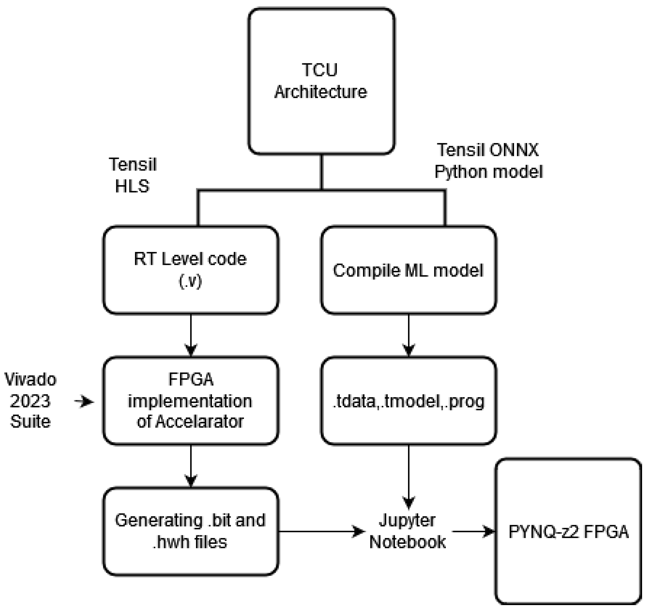
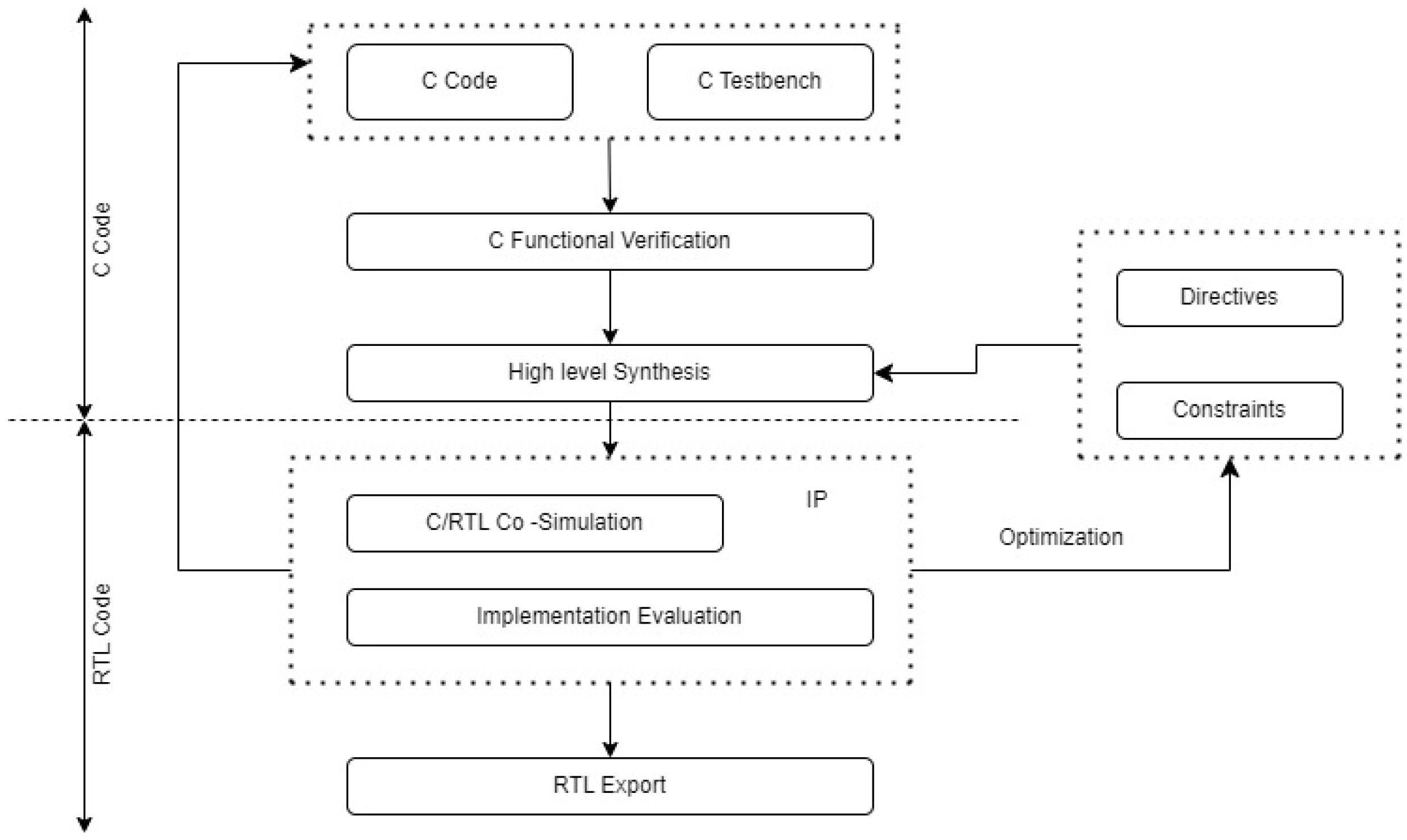
2.1. Design and Tensil Flow for RTL Code

In Figure 2, the Xilinx Vivado suite 2023 tool introduces a platform-based design flow, allowing the creation of hardware designs by importing the RTL code into an IP block and integrating it with other peripheral and PS/IP blocks. The Jupyter Notebook is the primary online computing environment for the PYNQ platform, which is connected to the Xilinx platforms. PYNQ is an FPGA-based Python application that runs on a Linux kernel. However, it should be noted that PYNQ does not fully support all Python libraries, which may result in some functionalities not working as expected.
From Figure 1, it is evident that the TCU RTL is generated from Tensil, which may initially be coded in C/C++ [14]. We then applied clock-gating techniques to the generated RTL code. The ML model, utilizing the Python ONNX format, performs image detection on the FPGA. This detailed process flow, which involves both high-level synthesis and low-level hardware optimizations, ensures efficient and effective implementation of CNN-based object detection on FPGA-SoC platforms.
After the simulation runs, we generated the bitstream (.bit and .hwh files) and imported it into the Jupyter Notebook, which operates in Python. For the model representation, we have chosen to use ONNX over TensorFlow. This distinction between the C/C++ HLS flow and the Python ONNX model is crucial to understanding our design process.
Tensil’s CNN accelerator is based on a systolic array architecture, as depicted in Figure 3. A systolic array consists of a grid of Processing Elements (PEs) that perform multiply–accumulate (MAC) operations, which are essential for CNN computations. Each PE in the array processes data synchronously, allowing for efficient computation of the convolutional layers [14]. In Figure 3, we illustrate the different modules within the Tensil accelerator, including the MAC units and inner dual-port RAM. Our optimizations involve applying clock-gating techniques, such as Local explicit clock gating (LECG) and Local explicit clock enable (LECE), to selectively reduce power consumption within these modules without compromising overall functionality. Specifically, LECG and LECE are applied to the BRAM modules surrounding the MAC units to enhance power efficiency [13].

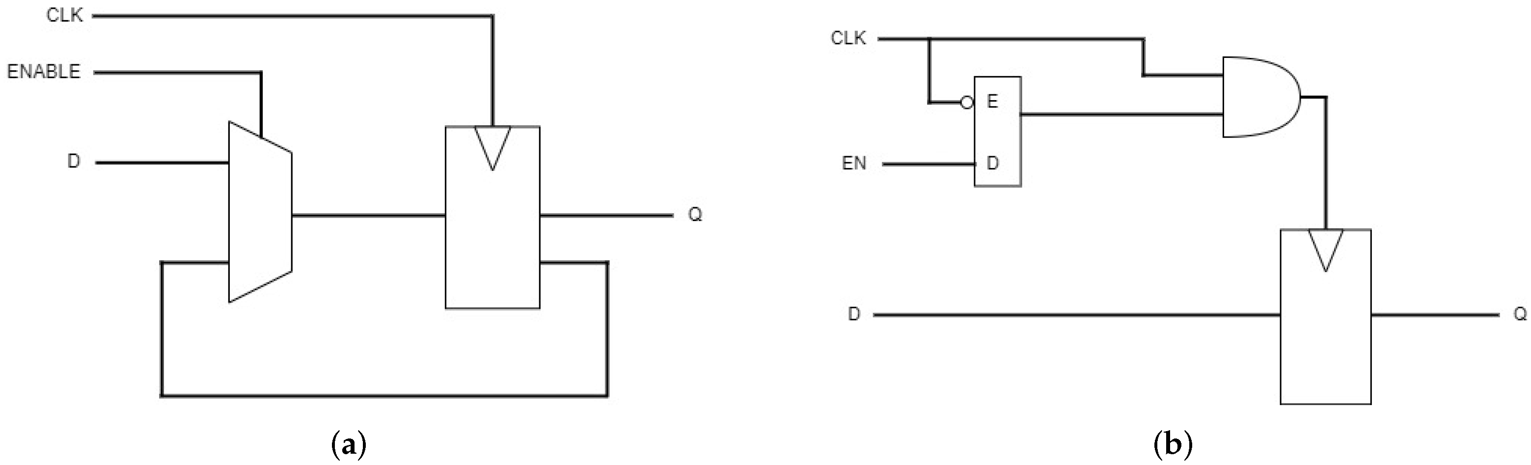
2.2. Clock-Gating Techniques

Clock gating (CG) is illustrated in Figure 4. This simple low-power method enhances efficiency and performance by turning off extra clock cycles. A significant portion of the computation process in the CNN involves standby states, resulting in substantial power consumption [16]. CG eliminates unnecessary clock cycle events, thereby reducing power consumption:
  • Local explicit clock enable (LECE): LECE updates the output on the clock’s rising edge, dependent on a high-enable signal [17]. It allows for precise control of clock-enabled signals, optimizing power consumption in synchronous digital circuits.
  • Local explicit clock gating (LECG): LECG optimizes power consumption by updating all the output at once, triggered by a clock-enable signal [17]. It efficiently gates the clock signals to reduce dynamic power consumption in digital circuits.
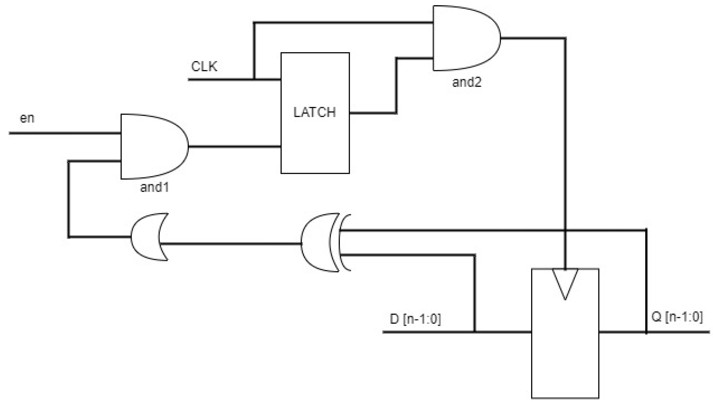
  • Enhanced clock gating (ECG): Figure 5 refers to clocking techniques tailored with the XOR gates to control the input clock signal and enable signals when considering multibit I/O data [18]. It optimizes the clock distribution and gating strategies to minimize power consumption while maintaining this structure and the timing requirements.
Figure 4. (a) Local explicit clock enable (LECE); (b) Local explicit clock gating (LECG).
Electronics 13 02676 g004
In a CNN accelerator, multiple modules collaborate to process the data and weights efficiently. Figure 3 illustrates the flow of the inputs through these modules. At the heart of the accelerator is the multiply and accumulate (MAC) module, which performs the core computations by multiplying the input data with the corresponding weights and accumulating the results. The data are buffered before and after the MAC operations using the Block RAM (BRAM) modules, positioned on either side of the MAC module. These BRAMs are available in various sizes, such as 2048 bits and 8192 bits, to support efficient data management. Once stored in the BRAMs alongside the weights, the data undergo processing within the MAC module before being returned to the BRAMs.

3. Proposed Design and Optimization

3.1. Implementation of the Original Design

We utilized Xilinx Vivado 2023 for the synthesis and implementation of the RTL. Vivado handles synthesis, error checking, place, and route and generates power and utilization summaries. The resulting bitstream configures the PYNQ-Z2 board and integrates seamlessly with the Python code to execute CNN-based object detection efficiently [14]. Our implementation included the original Tensil design [14], a previously proposed model [18], and our design on the PYNQ-Z2 FPGA using the Vivado 2023 suite. This approach enabled us to measure the impact of the optimizations accurately.

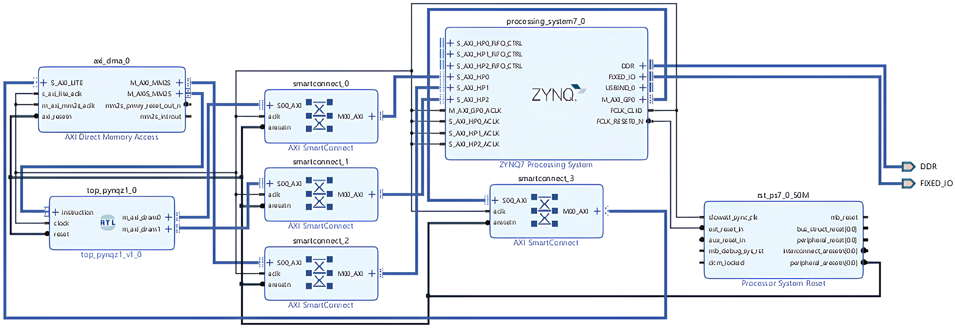
Tensil Clone and Module Integration

The Tensil open-source tool was cloned using the Docker and Verilog modules such as top-pynq.v, bram1, and bram2. These modules were integrated to form a custom IP block that serves as the core of the CNN accelerator. Figure 6 illustrates the connections between various IP blocks to ensure seamless communication with the FPGA board, including Zynq IP and API Smart Connects [16]. The ‘top-pynq’ module comprises several submodules, where low-power techniques are applied, including MACs, POOLs, CONV, InnerDualPort RAM, ALUs, and Counters [14]. Figure 7 presents the report of the utilization of the hardware components on the PYNQ-Z2 board after the synthesis and implementation completion.

3.2. Low-Power Techniques on Original Design

The previously proposed design [18] focuses on optimizing power consumption through the MAC module, which serves as a submodule within the ‘top-pynq’ module [18]. Figure 8 illustrates the functionality of the MAC module, typically involving two registers that each handle 16-bit values, performing individual multiplications and storing the results in another register. An adder then combines these results into high and low bits.
In the CNN architectures, the MAC unit for frequent data transmission is a significant power consumer. To mitigate this, unnecessary clock toggles are eliminated when the data input is inactive, as depicted in Figure 8. This strategy is facilitated by the Local explicit clock gating (LECG), which controls the clock, enabling the use of an XOR gate to prevent unnecessary toggling [16]. To ensure safe clock disabling and prevent glitches, an AND gate and latch have been incorporated, contrasting with traditional designs [18]. Figure 9 presents the hardware resource report for the PYNQ-Z2.

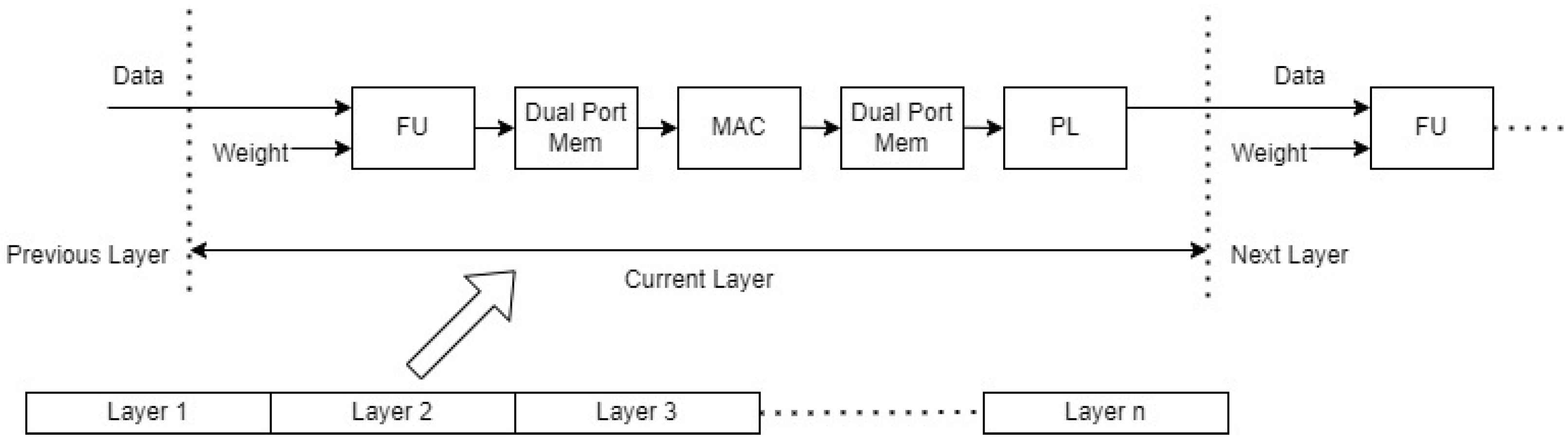
3.3. Proposed Hardware Implementation

Low-Power RTL Design

The Block RAM (BRAM) plays a critical role in CNN accelerators by serving as on-chip memory to store intermediate data, weights, and activations. This enables faster data access and reduced latency compared to accessing off-chip memory, which is more power-intensive. BRAMs are specifically used to hold weights and activations for various CNN layers, facilitating quick access during computation and minimizing the need for power-intensive off-chip memory accesses.
However, BRAM itself consumes significant power, prompting efforts to reduce consumption by applying the Low-Energy clock gating (LECG) technique within the BRAM and MAC modules. In our ‘top-pynq’ module, we employed two types of BRAM: one with a size of 2048 bits and another with 8192 bits. Implementing LECG and Local explicit clock enable (LECE) techniques in these BRAMs and Inner Dual-Port Memory contributes to power reduction significantly. By strategically utilizing Inner Dual-Port Memory and BRAMs with power-saving measures like LECG and LECE, we achieve a balance between high performance and energy efficiency within CNN hardware accelerators.
LECG involves controlling the clock signal through an enable signal using a latch and AND gate mechanism. In our ‘top-pynq’ module, which includes dual-port RAMs, registers A and B are managed similarly: the clock is activated only when the enable signal for each register is high, allowing efficient write operations. This approach eliminates unnecessary clock toggles, ensuring that only essential circuitry is active at any given time, thus reducing overall power consumption.
The Inner Dual-Port RAM module also employs LECE to regulate data transfer to registers. The data are transferred to registers only when the enable signal is high, and the latch maintains its state when the signal is low, achieved through a multiplexer. This method effectively manages the data flow, minimizing unnecessary power consumption when registers are idle. Implementing LECE improves the overall design efficiency by optimizing the data flow and power usage.
Table 1 provides an implementation of the LECG design compared with the ECG and the original design, demonstrating significant reductions in flip-flops and power consumption. We applied the LECG and LECE techniques in the MAC, Inner Dual-Port RAM, and BRAM modules, highlighting their effectiveness in optimizing power usage across various components.
Our CNN accelerator operates with a fixed-point bandwidth of 16 bits. Through thorough analysis, we have optimized the RTL code to enhance flexibility and facilitate the implementation of our accelerator design. The reduced number of Lookup Tables (LUTs) and Digital Signal Processors (DSPs) in our design can be attributed to the effective application of clock-gating techniques such as Local explicit clock enable (LECE) and Local explicit clock gating (LECG). These techniques minimize switching activity within the FPGA, directly influencing LUT and DSP utilization. We can maximize FPGA resource efficiency by activating necessary logic blocks and deactivating idle ones. This optimized resource utilization reduces the hardware footprint required for computational tasks and contributes to the lower power consumption and enhanced performance of our CNN accelerator.

4. Experiment and Results

4.1. Formality Check

Formality [20] is a Synopsys tool that determines if the original and implemented designs are equivalent. That means it compares the two designs to see if they accomplish the same tasks. Formality allows us to ensure that the application of clock gating does not alter the functionality of the original design. Formality was effectively applied to verify the implemented design, as shown in Figure 10, similar to ensuring that everything keeps functioning as it should after making changes.

4.2. Power Results

Our proposed design leads to a 22% decrease in dynamic power consumption and a 25% reduction in total on-chip power, as shown in Figure 11. Additionally, this approach can handle strong fan-out signals, guaranteeing the operation of the device. Furthermore, device speed can be increased by adding intermediate flip-flops to the pipeline logic; however, using too many flip-flops increases the computational complexity. Our low-power methods surpass flip-flop-based methods in terms of performance.

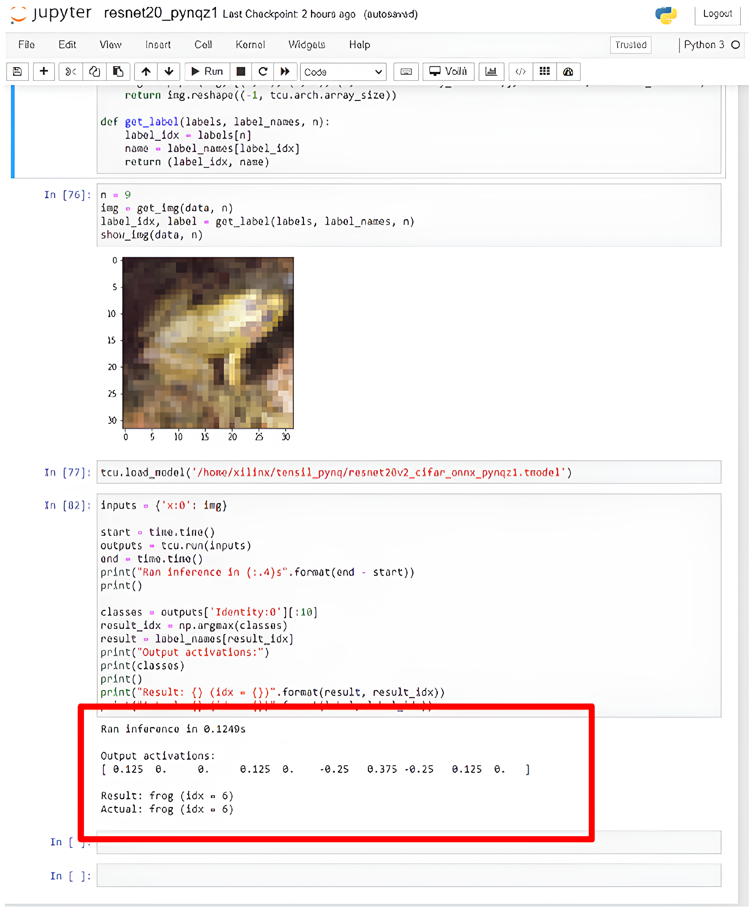
4.3. PYNQ Board Setup

We chose the PYNQ-Z2 board over the ZYNQ-7020 board for our foundational hardware platform because it is open-source and integrates the Xilinx PYNQ-Z2 with a framework based on Jupyter. The FPGA-SoC architecture of the PYNQ-Z2 includes a processing system (PS) and Programmable Logic (PL). Our main tool for software development was the Jupyter Notebook, which supports libraries like OpenCV and the Python and C/C++ programming languages. The ResNet-20 CNN architecture [21], trained on the CIFAR-10 dataset, was used in our experimental setup. The ONNX model converter was utilized to convert the weights into the ONNX format. Three essential artifacts, .tmodel, .tdata, and .tprog, from the Tensil compiler are used by the CNN driver to locate the binary files, program data, and weighted data, and they are not changed, indicating that the accuracy is the same as compared to the original. Figure 12 illustrates the Jupyter environment and the object-detection results achieved through testing on the PYNQ board.

5. Discussion

We confirmed that more register buffers are activated for our suggested structure compared to the previous result [18]. The structure can be changed through RTL code modification after we verify the functionality and performance of the design. After that, we can enhance the design’s power usage and hardware specifications. By analyzing the outcome, CNN processing performs better. Figure 11 illustrates how the processing system unit’s power consumption has decreased. As a power efficiency result, we were able to archive the 43.9 (GOPs/W), which increased 1.37-times over other FPGA board implementations [11,18]. In contrast to the original design [14], our design result showed a reduction of 22% dynamic power.
O r i g i n a l P o w e r = 1.714 W a t t s
P r o p o s e d d e s i g n p o w e r = 1.331 W a t t s
P o w e r r e d u c t i o n = 1.714 1.331 1.714 × 100 = 22.34 %
The clock frequency in our design was set to run at 50 MHz. This parameter sets the clock signal’s cycle rate, representing the speed at which the digital system’s operations are carried out.
Each BRAM block in this FPGA is [19]. The Xilinx PYNQ-Z2 board is based on the Zynq-7000 series SoC and typically has a size of 36 Kb (kilobits), which is 4.5 KB (kilobytes) per block. So, multiplying the number of BRAM blocks used by the size of each BRAM block, our design uses 44 BRAM blocks, then the total BRAM memory used is calculated as follows:
T o t a l B R A M m e m o r y u s e d ( kB ) = 44 × 4.5 kB = 198 kB
The total time it takes for an operation to finish is called latency, commonly expressed in clock cycles and clock periods. It is computed as the product of the clock period—the length of each clock cycle—and the number of clock cycles needed for the operation [11]. Latency measurements were conducted using a Jupyter Notebook in Python. In our experimental setup, we sequentially processed images through the CNN accelerator, recording the runtime for each image from the start of the prediction process to the final output. This approach ensured that we accurately captured the end-to-end latency for each image. We averaged the runtime across multiple images to obtain a reliable measure of the accelerator’s latency.
In a CNN, latency is inversely correlated with frames per second (FPS) [11]. FPS is the number of frames the network processes in a second, whereas latency is the total time it takes the network to process a single frame. The observed latency was approximately 0.102 s. From this latency, we can calculate the number of frames processed per second (FPS). Therefore, the accelerator module operates at approximately 9.803 frames per second.
F r a m e s p e r s e c o n d ( F P S ) = 1 L a t e n c y
The rate of processing operations in CNNs is known as throughput, and it is commonly expressed in giga-operations per second (GOPS) [18]. In real-time tasks, computational efficiency is of utmost importance [11]. GOPS are optimized through various methods like hardware acceleration and model parallelism, representing billions of operations completed in a single second. The computational workload of a CNN is determined by summing the MAC operations across all network layers. Applying ECG to the MAC module, as done in our previous publication [18], results in a total of 6.97 billion MAC operations observed in our current study. This metric serves as the basis for calculating our system’s GOPS, reflecting the efficiency and throughput of our CNN implementation.
Table 2 represents a comprehensive comparison between our design and previously proposed solutions, focusing on key performance metrics including power consumption, throughput, latency, and power efficiency. This analysis offers insights into the advancements achieved by our approach relative to existing methodologies, highlighting areas of improvement.
Our study focuses on demonstrating superior power efficiency across various CNN architectures deployed on FPGA accelerators. We highlight distinct efficiencies achieved through FPGA optimization techniques by comparing power consumption among ResNet20, VGG16, and A2pDnet models. Despite variations influenced by factors like image size and chip technology, our findings underscore the efficacy of our approach in enhancing power performance across different architectural complexities. This comparative analysis aims to establish actionable insights for future FPGA-based accelerator designs in object-detection applications. In advancing this research, we anticipate challenges related to stringent timing constraints, particularly as we expand our exploration to more complex architectures. Addressing these challenges will require subtle adjustments and optimizations to ensure efficient performance and power usage.

6. Conclusions

The highly reconfigurable FPGA hardware accelerator suggested in this article outperformed other hardware regarding processing speed and power consumption when running different CNNs. The main objectives of the hardware optimization were to reduce power consumption and increase throughput. We used low-power techniques at the RT level in addition to controlling data access to minimize memory access to achieve energy-efficient CNN object detection. These included an OR-based MAC architecture, bus-specific clocking, and the LECE and LECG techniques on Inner Dual-Port RAM and BRAM modules. The PYNQ-Z2 mobile FPGA-SoC was used to implement the suggested hardware accelerator for ResNet-20, and power consumption was monitored during inference. The outcomes revealed a 22.31% reduction in power consumption, a 55% increase in hardware utilization, and a 19% rise in throughput over the original design. This enables real-time processing on an FPGA, with an object-detection processing speed of 9.803 frames per second (FPS).

Author Contributions

Conceptualization, data curation, formal analysis, investigation, methodology, validation, A.G. and Y.A.S.; writing—original draft, writing—review and editing, N.A.; supervision, funding acquisition, project administration, K.K.C. All authors read and agreed to the published version of the manuscript.

Funding

This work was supported by the Technology Innovation Program (20018906, Development of autonomous driving collaboration control platform for commercial and task assistance vehicles) funded By the Ministry of Trade, Industry and Energy (MOTIE, Republic of Korea).

Data Availability Statement

Dataset available on request from the authors. The raw data supporting the conclusions of this article will be made available by the authors on request.

Acknowledgments

We thank our colleagues from KETI and KEIT, who provided insight and expertise, which greatly assisted the research and improved the manuscript.

Conflicts of Interest

The authors declare no conflicts of interest.

Abbreviations

The following abbreviations are used in this manuscript:
ECGEnhanced clock gating
LECGLocal explicit clock gating
IPIntellectual Property Blocks
BRAMBlock Random Access Memory
CONVConvolution Layer
MACmultiply and accumulate
RTLregister transfer level
CNNconvolutional neural networks
FPGAfield-programmable gate array
HLShigh-level synthesis
SocSystem-on-Chip
ONNXOpen Neural Network Exchange

References

  1. Jameil, A.K.; Al-Raweshidy, H. Efficient CNN Architecture on FPGA Using High Level Module for Healthcare Devices. IEEE Access 2022, 10, 60486–60495. [Google Scholar] [CrossRef]
  2. Zhang, Z.; Mahmud, M.A.P.; Kouzani, A.Z. FitNN: A Low-Resource FPGA-Based CNN Accelerator for Drones. IEEE Internet Things J. 2022, 9, 21357–21369. [Google Scholar] [CrossRef]
  3. Li, X.; Gong, X.; Wang, D.; Zhang, J.; Baker, T.; Zhou, J.; Lu, T. ABM-SpConv-SIMD: Accelerating Convolutional Neural Network Inference for Industrial IoT Applications on Edge Devices. IEEE Trans. Netw. Sci. Eng. 2023, 10, 3071–3085. [Google Scholar] [CrossRef]
  4. Nikouei, S.Y.; Chen, Y.; Song, S.; Xu, R.; Choi, B.Y.; Faughnan, T.R. Smart Surveillance as an Edge Network Service: From Harr-Cascade, SVM to a Lightweight CNN. arXiv 2018, arXiv:1805.00331. [Google Scholar]
  5. Tamimi, S.; Ebrahimi, Z.; Khaleghi, B.; Asadi, H. An Efficient SRAM-Based Reconfigurable Architecture for Embedded Processors. IEEE Trans. Comput. Aided Des. Integr. Circuits Syst. 2019, 38, 466–479. [Google Scholar] [CrossRef]
  6. Wu, X.; Ma, Y.; Wang, M.; Wang, Z. A Flexible and Efficient FPGA Accelerator for Various Large-Scale and Lightweight CNNs. IEEE Trans. Circuits Syst. Regul. Pap. 2022, 69, 1185–1198. [Google Scholar] [CrossRef]
  7. Irmak, H.; Ziener, D.; Alachiotis, N. Increasing Flexibility of FPGA-based CNN Accelerators with Dynamic Partial Reconfiguration. In Proceedings of the 2021 31st International Conference on Field-Programmable Logic and Applications (FPL), Dresden, Germany, 30 August–3 September 2021; pp. 306–311. [Google Scholar] [CrossRef]
  8. Wei, Z.; Arora, A.; Li, R.; John, L. HLSDataset: Open-Source Dataset for ML-Assisted FPGA Design using High Level Synthesis. In Proceedings of the 2023 IEEE 34th International Conference on Application-Specific Systems, Architectures and Processors (ASAP), Porto, Portugal, 19–21 July 2023; pp. 197–204. [Google Scholar] [CrossRef]
  9. Mohammadi Makrani, H.; Farahmand, F.; Sayadi, H.; Bondi, S.; Pudukotai Dinakarrao, S.M.; Homayoun, H.; Rafatirad, S. Pyramid: Machine Learning Framework to Estimate the Optimal Timing and Resource Usage of a High-Level Synthesis Design. In Proceedings of the 2019 29th International Conference on Field Programmable Logic and Applications (FPL), Barcelona, Spain, 8–12 September 2019; pp. 397–403. [Google Scholar] [CrossRef]
  10. Ullah, S.; Rehman, S.; Shafique, M.; Kumar, A. High-Performance Accurate and Approximate Multipliers for FPGA-Based Hardware Accelerators. IEEE Trans. Comput. Aided Des. Integr. Circuits Syst. 2022, 41, 211–224. [Google Scholar] [CrossRef]
  11. Li, S.; Luo, Y.; Sun, K.; Yadav, N.; Choi, K.K. A Novel FPGA Accelerator Design for Real-Time and Ultra-Low Power Deep Convolutional Neural Networks Compared with Titan X GPU. IEEE Access 2020, 8, 105455–105471. [Google Scholar] [CrossRef]
  12. Yang, C.; Wang, Y.; Zhang, H.; Wang, X.; Geng, L. A Reconfigurable CNN Accelerator using Tile-by-Tile Computing and Dynamic Adaptive Data Truncation. In Proceedings of the 2019 IEEE International Conference on Integrated Circuits, Technologies and Applications (ICTA), Chengdu, China, 13–15 November 2019; pp. 73–74. [Google Scholar] [CrossRef]
  13. Zhang, X.; Ma, Y.; Xiong, J.; Hwu, W.M.W.; Kindratenko, V.; Chen, D. Exploring HW/SW Co-Design for Video Analysis on CPU-FPGA Heterogeneous Systems. IEEE Trans. Comput. Aided Des. Integr. Circuits Syst. 2022, 41, 1606–1619. [Google Scholar] [CrossRef]
  14. Tensil. Learn Tensil with ResNet and PYNQ Z1. Available online: https://www.tensil.ai/docs/tutorials/resnet20-pynqz1/ (accessed on 15 December 2022).
  15. Kim, Y.; Tong, Q.; Choi, K.; Lee, E.; Jang, S.J.; Choi, B.H. System Level Power Reduction for YOLO2 Sub-modules for Object Detection of Future Autonomous Vehicles. In Proceedings of the 2018 International SoC Design Conference (ISOCC), Daegu, Republic of Korea, 12–15 November 2018; pp. 151–155. [Google Scholar] [CrossRef]
  16. Kim, Y.; Kim, H.; Yadav, N.; Li, S.; Choi, K.K. Low-Power RTL Code Generation for Advanced CNN Algorithms toward Object Detection in Autonomous Vehicles. Electronics 2020, 9, 478. [Google Scholar] [CrossRef]
  17. Kim, H.; Choi, K. Low Power FPGA-SoC Design Techniques for CNN-based Object Detection Accelerator. In Proceedings of the 2019 IEEE 10th Annual Ubiquitous Computing, Electronics and Mobile Communication Conference (UEMCON), New York, NY, USA, 10–12 October 2019; pp. 1130–1134. [Google Scholar] [CrossRef]
  18. Kim, V.H.; Choi, K.K. A Reconfigurable CNN-Based Accelerator Design for Fast and Energy-Efficient Object Detection System on Mobile FPGA. IEEE Access 2023, 11, 59438–59445. [Google Scholar] [CrossRef]
  19. Advanced Micro Devices, Inc. AMD PYNQ-Z2. Available online: https://www.amd.com/en/corporate/university-program/aup-boards/pynq-z2.html (accessed on 19 June 2024).
  20. Synopsys. End-to-End Verification of Low Power Designs. 2020. Available online: https://www.synopsys.com/content/dam/synopsys/verification/white-papers/verification-e2e-low-power-wp.pdf (accessed on 1 April 2024).
  21. Zhang, Y.; Tong, Q.; Li, L.; Wang, W.; Choi, K.; Jang, J.; Jung, H.; Ahn, S.Y. Automatic Register Transfer level CAD tool design for advanced clock gating and low power schemes. In Proceedings of the 2012 International SoC Design Conference (ISOCC), Jeju Island, Republic of Korea, 4–7 November 2012; pp. 21–24. [Google Scholar] [CrossRef]
  22. Gong, L.; Wang, C.; Li, X.; Chen, H.; Zhou, X. MALOC: A Fully Pipelined FPGA Accelerator for Convolutional Neural Networks with All Layers Mapped on Chip. IEEE Trans. Comput. Aided Des. Integr. Circuits Syst. 2018, 37, 2601–2612. [Google Scholar] [CrossRef]
  23. Bai, L.; Zhao, Y.; Huang, X. A CNN Accelerator on FPGA Using Depthwise Separable Convolution. IEEE Trans. Circuits Syst. II Express Briefs 2018, 65, 1415–1419. [Google Scholar] [CrossRef]
  24. Qiu, J.; Wang, J.; Yao, S.; Guo, K.; Li, B.; Zhou, E.; Yu, J.; Tang, T.; Xu, N.; Song, S.; et al. Going Deeper with Embedded FPGA Platform for Convolutional Neural Network. In Proceedings of the 2016 ACM/SIGDA International Symposium on Field-Programmable Gate Arrays, New York, NY, USA, 21–23 February 2016; FPGA ’16. pp. 26–35. [Google Scholar] [CrossRef]
  25. Geng, T.; Wang, T.; Sanaullah, A.; Yang, C.; Patel, R.; Herbordt, M. A Framework for Acceleration of CNN Training on Deeply-Pipelined FPGA Clusters with Work and Weight Load Balancing. In Proceedings of the 2018 28th International Conference on Field Programmable Logic and Applications (FPL), Dublin, Ireland, 27–31 August 2018; pp. 394–3944. [Google Scholar] [CrossRef]
  26. Guan, Y.; Liang, H.; Xu, N.; Wang, W.; Shi, S.; Chen, X.; Sun, G.; Zhang, W.; Cong, J. FP-DNN: An Automated Framework for Mapping Deep Neural Networks onto FPGAs with RTL-HLS Hybrid Templates. In Proceedings of the 2017 IEEE 25th Annual International Symposium on Field-Programmable Custom Computing Machines (FCCM), Napa, CA, USA, 30 April–2 May 2017; pp. 152–159. [Google Scholar] [CrossRef]
  27. Ma, Y.; Cao, Y.; Vrudhula, S.; Seo, J.S. Optimizing the Convolution Operation to Accelerate Deep Neural Networks on FPGA. IEEE Trans. Very Large Scale Integr. Syst. 2018, 26, 1354–1367. [Google Scholar] [CrossRef]
Figure 1. Design architecture.
Electronics 13 02676 g001
Figure 2. HLS flow in Vivado.
Electronics 13 02676 g002
Figure 3. CNN accelerator computation process and each module.
Electronics 13 02676 g003
Figure 5. Enhanced clock gating (ECG).
Electronics 13 02676 g005
Figure 6. IP block design of CNN accelerator.
Electronics 13 02676 g006
Figure 7. HW resource report of original design [14].
Electronics 13 02676 g007
Figure 8. ECG MAC unit design.
Electronics 13 02676 g008
Figure 9. HW resource report of MAC design [18].
Electronics 13 02676 g009
Figure 10. Formality.
Electronics 13 02676 g010
Figure 11. HW resource report of our work on PYNQ FPGA.
Electronics 13 02676 g011
Figure 12. PYNQ board results in Jupyter environment.
Electronics 13 02676 g012
Table 1. Comparison results of different low-power techniques.
CG Techniques [16]PYNQ-Z2 Hardware [19]Original [14]ECG [18]LECG and LECE
LUTs53 k14.6 k15.6 k12.2 k
BRAMs (kB)630198523198
DSPs2207316765
FFs85 k9.1 k41.2 k10.45 k
Dynamic Power (W)-1.7141.4401.331
Table 2. Comparison results of FPGA implementation.
Year2018 [22]2018 [23]2018 [24]2018 [25]2017 [26]2018 [27]2019 [11]2022 [14]2022 [18]2024 Proposed
CNN modelAlexNetMobileNet V2VGG16VGG16VGG19VGG16AP2D-NetResNet20ResNet20ResNet20
FPGAZYNQ-XCZ7020Intel Arria 10-SoCZYNQ-XCZ7020Virtex-7 VX690tStratix V GSMDSIntel Arria 10Ultra96PYNQ-Z1PYNQ-Z1PYNQ-Z2
LUTs49.8 k-29.9 k---54.3 k14.6 k15.2 k12.2 k
BRAMs (kB)268184485.512209192232162198523198
DSPs21812781902160103615182877316765
Precision (W,A)(16,16)(16,16)(8,8)(16,16)(16,16)(16,16)(8–16,16)(16,16)(16,16)(16,16)
Clock (MHz)200133214150150200300505050
Latency (s)0.0160.0040.3640.1060.1070.0430.0320.1780.1090.102
Throughput (GOPS)80.35170.684.3290364.4715.9130.25563.368.4
Power (W)2.21--3525-5.591.7141.4401.331
Power Efficiency (GOPS/W)36.36--8.2814.57-23.328.243.951.38
Disclaimer/Publisher’s Note: The statements, opinions and data contained in all publications are solely those of the individual author(s) and contributor(s) and not of MDPI and/or the editor(s). MDPI and/or the editor(s) disclaim responsibility for any injury to people or property resulting from any ideas, methods, instructions or products referred to in the content.

