Article

Digital Functional Blocks Implementation of PWM and Control for a High-Frequency Interleaved Y-Inverter Motor Drive

1
Solid-State Power Processing (SP2) Lab, Kyoto University of Advanced Science, Kyoto 615-8577, Japan
2
Nagamori Institute of Actuators, Kyoto University of Advanced Science, Kyoto 615-8577, Japan
*
Author to whom correspondence should be addressed.
Electronics 2024, 13(13), 2610; https://doi.org/10.3390/electronics13132610
Submission received: 30 April 2024 / Revised: 22 June 2024 / Accepted: 26 June 2024 / Published: 3 July 2024
(This article belongs to the Special Issue Digital Control of Power Electronics)

Abstract

This paper is about the development and demonstration of a motor drive for e-transport applications based on an innovative hybrid Si-SiC dual switching frequency interleaved buck–boost Y-inverter and a single-rotor Halbach machine. In particular, the focus is the implementation of the required discontinuous inverter modulation scheme, input voltage feed-forward and motor currents feedback control loops, as well as over-voltage, over-current, and over-temperature protections, using an off-the-shelf commercial hardware platform enabling straightforward Simulink-environment programming of all parts, while ensuring the high switching frequency capability required by wide-band-gap semiconductors. Experimental results showed good inverter efficiency, transient dynamic response to load changes, input voltage regulation, and fully functional protection capability, validating the proposed approach as a powerful option for reducing system development time and cost.

1. Introduction

Until recently, the prevailing trajectory in the development of traction drives for hybrid and fully electric vehicles (EVs) emphasized increasing primary source voltage levels to reach state-of-the-art bus values of 800 V for power ratings in excess of 100 kW. Such high voltages facilitate the creation of traction drive systems relying solely on an inverter to feed the machine, without the necessity for voltage step-up DC–DC converters on the input side. Recently, however, a trend reversal has been emerging, marked by a considerable reduction in power and, consequently, input voltage ratings [1]. Now, future development is expected to focus more on ways to optimize the volume and weight of the motor by increasing the number of poles in the machine design, and thus increasing the required fundamental frequency and amplitude of the supply voltage, starting from a lower input battery voltage. In relation to that, interest in the adoption of wide-band-gap (WBG) semiconductors is also increasing, as they allow high switching frequencies and high efficiencies even at higher voltage ratings. So, in an effort to compensate the issue of a higher initial cost of the technology, benefits and savings in other parts of the system are being sought for by WBG bespoke designs. A promising solution that emerged within this context, and which is rapidly gaining widespread interest, is the Y-inverter, illustrated in Figure 1. The inverter consists of three DC–DC converters (Figure 1a) that are not modulated with a constant duty-cycle as is usual, but rather with a sinusoidally varying duty-cycle, as illustrated in Figure 1b: this way, each converter synthesizes an output voltage that is still non-zero DC-average, but is obtained from an offset sinusoidal waveform. When the output voltage is higher than the input voltage, the converter operates in boost mode; vice-versa, when the output voltage is lower than the input, the converter operates in buck mode. Via connecting three 120 deg phase-shifted sinusoidally-modulated DC–DC converter cells in Y-configuration as per Figure 1a, the DC offset at the output of each cell is cancelled out in the phase-to-phase or phase-to-neutral voltages of a three-phase load, yielding the required supply voltages and currents for a three-phase machine (Figure 1c). The amplitude of the phase-to-neutral voltage is indicated as VPN,PEAK in Figure 1b; provided that VPN,PEAK > VDC,IN (i.e., VOUT,PEAK > 2 × VDC,IN), then the boost capability of the load voltage relative to the input is ensured. In principle, various DC–DC converter topologies can be selected [2,3,4]; in this work, reference is made to the use of a four-switch non-inverting buck–boost architecture, the solution enabling the highest volumetric and gravimetric power density.
The advantages of Y-inversion over the conventional DC–DC boost plus step-down voltage-source inverter (VSI) approach are many-fold [2,3,4,5,6]:
No bulky and reliability critical DC-link capacitor is required;
Voltage boost capability is inherently possible;
Output electro-magnetic signature is greatly improved, both in terms of harmonic content and dV/dt values;
Switching losses are greatly reduced, enabling much higher switching frequencies;
Selection and operation of input- and output-side devices can be tailored to optimum performance and cost in terms of semiconductor technology, voltage rating, and switching frequency.
A detailed benchmark can be found in [7,8].
In this paper, a motor drive with a nominal rating of 7.5 kW is considered, supplied by a primary battery with a 60 V nominal rating (48 V min; 72 V max). These specifications were derived from an actual commercial light electric vehicle. To demonstrate major improvements in overall power density, a single-rotor Halbach machine was custom designed with a high number of poles and minimum inductances, requiring fundamental electrical frequencies up to about 2 kHz, with phase-to-neutral voltage amplitudes up to 120 V [9].

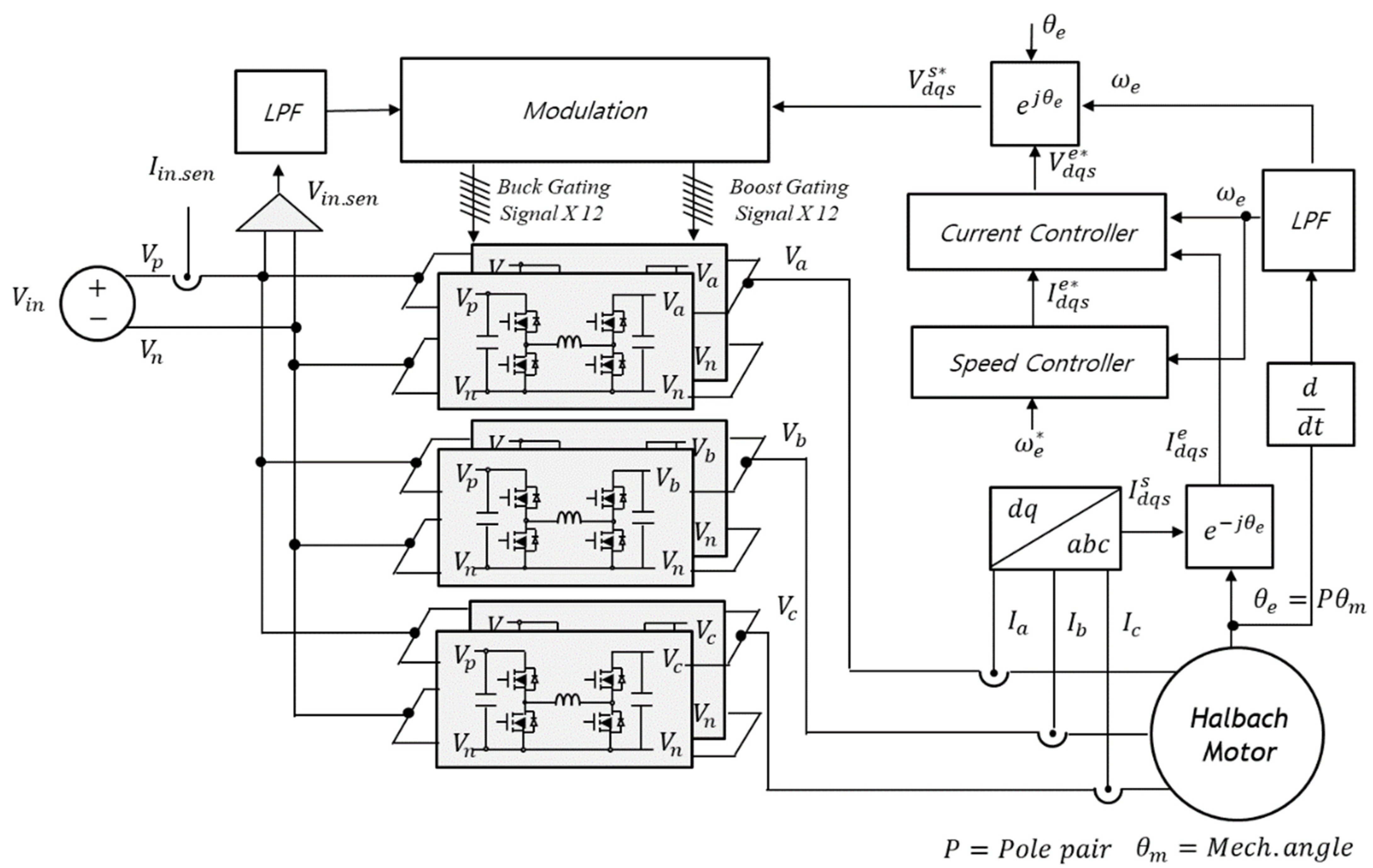
2. Inverter Architecture

2.1. Power Cell Design

The basic cell architecture is shown in Figure 2: a four-switch non-inverting buck–boost converter. As mentioned above, the voltage of the output capacitor is a combination of a DC and an AC voltage component, with the DC voltage offset being removed in a three-phase connection.
In view of the ratings detailed above, input-side transistors can be rated for relatively low voltage (e.g., 100 V). So, either silicon (Si) MOSFETs or gallium nitride (GaN) HEMTs could be chosen. Here, the choice was Si to contain cost. On the output side, 650 V-rated devices are ideal, so that both GaN HEMTs and silicon carbide (SiC) MOSFETs can be considered. Here, SiC MOSFETs were chosen by virtue of their greater maturity and availability from multiple manufacturers. To meet the overall current rating requirements, a single switch on the output was not sufficient. Rather than paralleling multiple devices, we opted for an interleaved implementation of a single cell, so as to reduce the size and electro-thermal stress of passive components. In particular, this design choice is compatible with the use of cross-coupled inductors, in which the equivalent magnetizing current can be significantly reduced [10].
As the Y-inverter’s boost stage has a higher current ripple than the buck’s leg, SiC MOSFET can be applied to the boost stage to strategically reduce ripple. In this paper, we discuss how to implement a three-phase motor system using a commercial hardware and software platform offering the possibility to implement high switching frequencies with extremely simple and straightforward functional block programming.

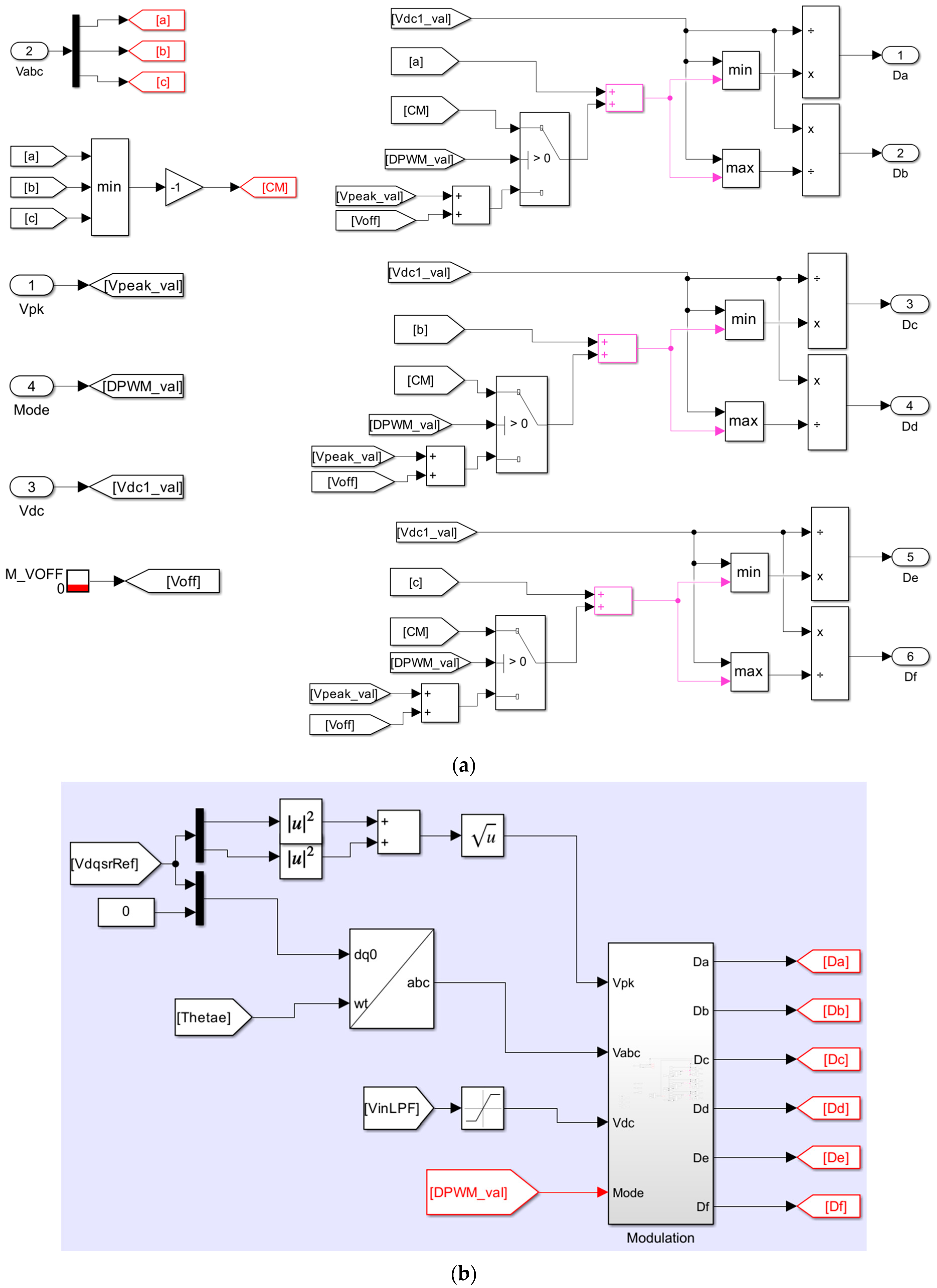
2.2. Modulation Strategy

With relevance to Figure 2, the relationship between the input voltage and the output voltage of one non-inverting buck–boost cell can be expressed as:
V a b c , n V p n = d B U 1 d B O = d B U d B O C = V ^ V p n · [ 1 + sin ( ω F t ) ]
where Vabc.n represents the output capacitor voltage of one of the three phases, and W, V, or U, and Vpn represent the input voltage. dBU is the duty ratio of the buck converter, dBO is that of the boost converter, and dBOC is its complementary (i.e., logic negation) signal.
Based on Equation (1), various modulation strategies are, in principle, possible. For instance:
-
Single-duty: If dBU = dBO = d, a single parameter modulation is achieved, with diagonal switch-pairs in the H-bridge cell jointly turned on and off;
-
Dual-duty: This is implemented by maintaining separate variable duty cycles for the buck and boost cells, setting dBU = 1 during boost-mode operation and, vice versa, setting dBOC = 1 during buck-mode operation;
-
Hybrid duty: Setting dBOC = k (with 0 < k < 1) and using only dBU as the control parameter means that the boost-side leg transistors are operated with constant duty and the buck-side ones with variable duty. Of course, the possibility to set a fixed dBU value and a variable dBOC also exists theoretically; however, in the case of sinusoidal modulation, the need to ensure 0 < dBOC < 1 implies increased complications.
A detailed comparison of various modulation schemes for the Y-inverter is beyond the scope of this paper, but the following observations can be made:
-
The dual-duty solution is the one enabling the lowest maximum voltage across the inductor and thus, the highest power density. Moreover, it minimizes switching losses, as only two devices are switching at any given time, allowing for maximum power density.
-
Single-duty modulation implements a continuous switching pattern of all devices, and thus, of the inductor current controllability; it can be of interest for ensuring good harmonic performance at relatively high output fundamental frequencies.
-
The hybrid-duty approach results in a fully linear control equation and can thus be of interest when a high-performance dynamic response is required while maintaining control simplicity.
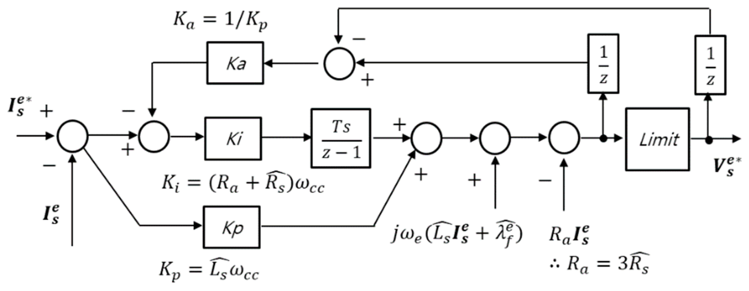
In this work, the dual-duty modulation approach is considered, with optimized different values for the switching frequencies of input and output switches.
In Figure 2, V d q is the command voltage required for the load phase voltage expressed in the d-q synchronous reference frame. The electrical angle (θ) can be obtained by multiplying the angular velocity (ω) by the sampling time (T) and the three-phase command voltage from the a-b-c stationary reference frame ( V a b c s ). The calculated three-phase command voltage requires the output capacitor voltage of each cell buck–boost converter with the magnitude of the command voltage as a DC offset to be applied to the load. Therefore, the offset voltage may be implemented by adding the magnitude of V d q to each of the three-phase command voltages, as also indicated in Figure 2. However, as errors in the practical implementation of the minimum voltage may occur due to resistance and sensing errors of the capacitor, it may be additionally corrected by an additional arbitrary v o ^ term. With this approach, sinusoidal PWM (SPWM) was implemented.
Next to SPWM, discontinuous PWM (DPWM) is also considered to reduce the output capacitor voltage peak of the Y-inverter and increase voltage utilization. This is also effective to boost efficiency, as switching is stopped for portions of the period. Here, specifically, a two-thirds discontinuous modulation (TTM) scheme was implemented, with reference voltages shown in Figure 3a, and the corresponding load voltages in Figure 3b. Figure 3c,d report estimated reductions in the boost-side transistors and cell inductor and output capacitor currents amplitudes by adopting SPWM or DPWM.
The selection of this specific DPWM scheme was made after extensive simulation-based benchmarks of the most common DPWM schemes [11,12], because TTM provides the highest efficiency in this particular application, enabling operation at the highest possible switching frequency, and thus with the smallest inductor value.

2.3. Control

Figure 4 illustrates the overall control diagram of the Si-SiC hybrid integrated Y-inverter developed in this study. It should be noted that to reduce the current stress on output capacitors, an interleaved configuration was chosen, as opposed to straightforward paralleling of transistors, to achieve the required current rating. So, each phase here consists of two parallel interleaved 180-degree switching frequency phase-shifted cells. Although not exploited here, such a solution also enables the use of cross-coupled inductors, further contributing to the power density optimization of the overall inverter. This solutions appears to increase the number of devices as compared to boost–VSI, but in reality it does not: the number of devices was chosen only to meet the required current rating, which was dictated by the requirement for the machine torque–speed characteristics to be just as high at low-speed high-torque conditions as the DC–DC converter boosting action makes them at high-speed low-torque conditions. So, for the same spec, a boost–VSI system would also likely be designed with interleaved cells in the boost stage to reduce the stress on the DC-link capacitor and parallel devices in the inverter stage.
To operate the motor, a cascaded controller that regulates the speed–phase current is required, utilizing the dq-axis frame as its reference. The controller relies on the electrical machine’s speed ω e , angle θe, and motor currents Ia, Ib, and Ic, and then generates the required AC voltages V a b c s that the inverter must produce at the machine’s terminals. The required AC motor voltages, including the DC offset voltage, can be generated based on each phase-leg buck–boost converter. Typically, controlling the output voltage of a buck–boost converter requires sensing the output voltage and DC inductor current. Usually, we consider comprising a cascaded output voltage inductor current controller [2]. However, due to its low output capacitance value, the Y-inverter allowed the design of current control using current sensors only if the motor control was compatible with a relatively narrow bandwidth (or slow) response. Nevertheless, in applications such as electric vehicles or systems requiring robust failure tolerance, the design of an interleaved structure proves advantageous. A robust response from the current controller is essential to address hardware imbalances arising from a single-leg failure. Furthermore, when dealing with a low-inductance-based motor featuring a high number of poles, the benefits of wide-band-gap semiconductors-based high switching frequency must be maximized with a fast response controller.
In order to prevent instability in the designed current controller resulting from parameter errors or other disturbances like digital delay and inverter nonlinearity, it was crucial to incorporate a virtual resistor, a technique commonly referred to as the active damping method. With the virtual resistor, the d- and q-axes equivalent circuits in the synchronous reference frame can be deduced, as shown in Figure 5.
[ v d s e v q s e ] = [ R v + R s + s L d s ω e L q s ω e L d s R v + R s + s L q s ] [ i d s e i q s e ] + [ 0 ω e λ f e ]  
  [ v d s e v q s e ] = [ K p d s + K i d s 0 0 K p q s + K i q s ] [ i d s e i d s e i q s e i q s e ] + [ 0 ω e L q s ^ ω e L d s ^ 0 ] [ i d s e i q s e ] + [ 0 ω e λ f e ^ ] R a [ i d s i q s ]
In (3), if P gains ( K p d ,   K p q ) are set as ( L d s ^ ω c c ,   L q s ^ ω c c ), I gains ( K i d ,   K i q ) are set as ( R s ^ + R v ) ω c c , and the virtual resistor ( R v = R a ) is set as ( 3 ~ 10 ) R s ^ , then the closed loop transfer function can be summarized as a first-order low pass filter between the desired currents ( i d s e ,   i q s e ) and the response currents ( i d s e ,   i q s e ) with the estimated motor inductances ( L d s ^ ,   L q s ^ ) and estimated linkage flux ( λ f e ^ ) well matched to the real plant. Based on (3), the current controller was designed as shown in Figure 6, and the anti-windup limiter was considered together with it to limit the output voltage. Here, the anti-windup control gain ( K a ) is as ( 1 / K p d ,   1 / K p q ). The modulation technique used here configured the controller by applying a method devised in a previous study [5].

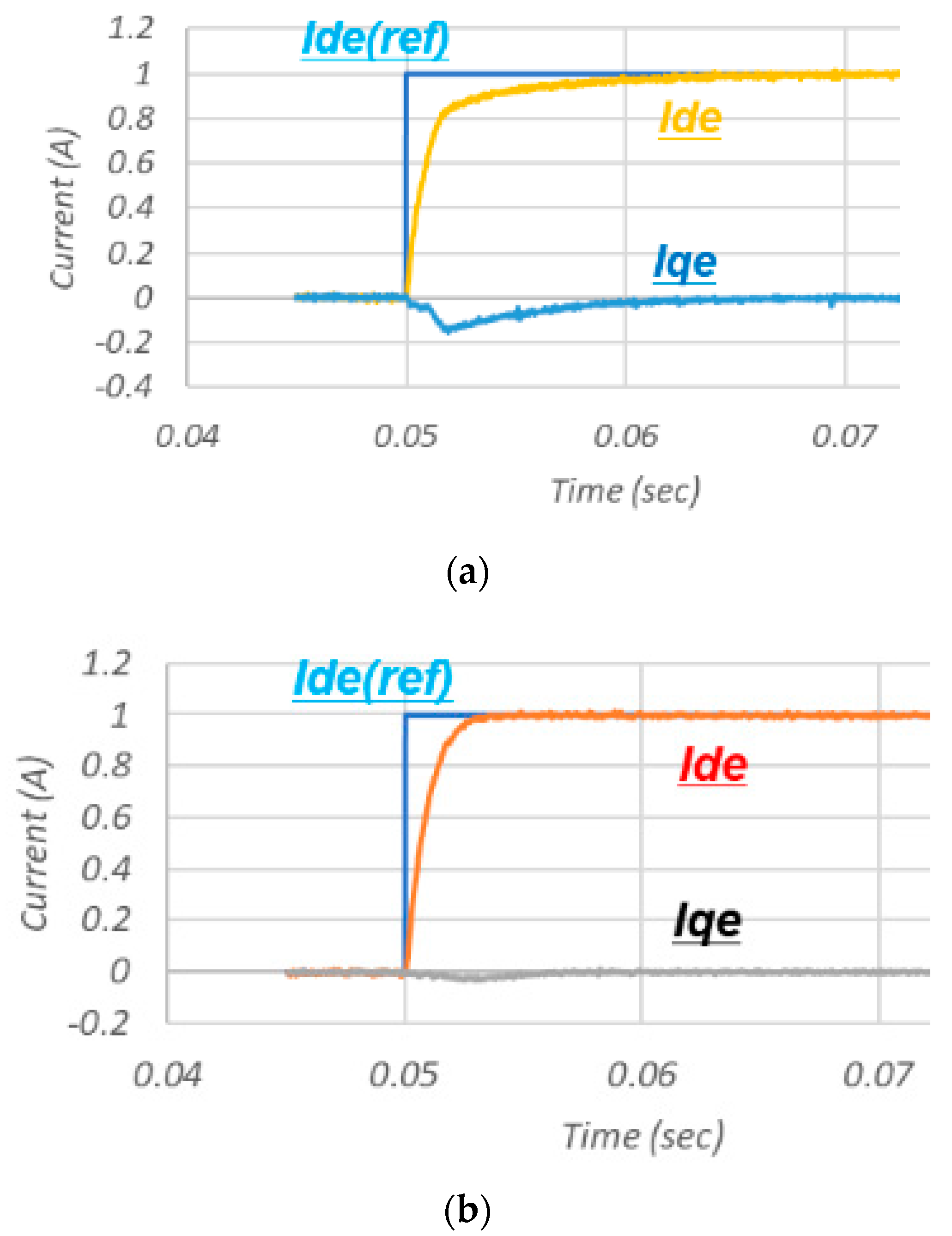
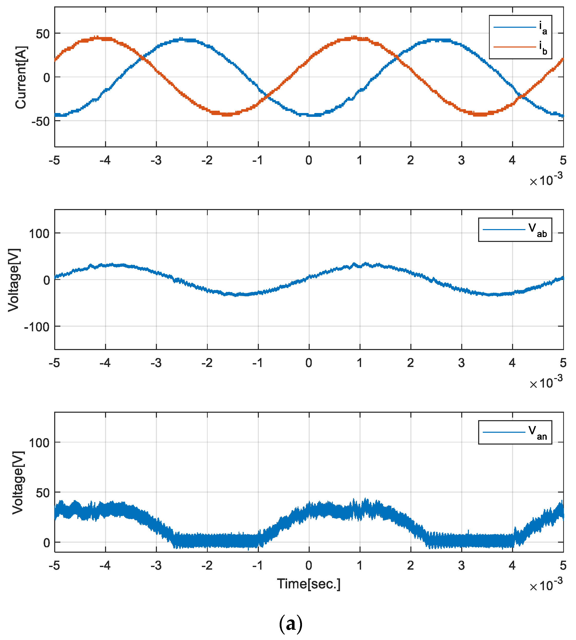
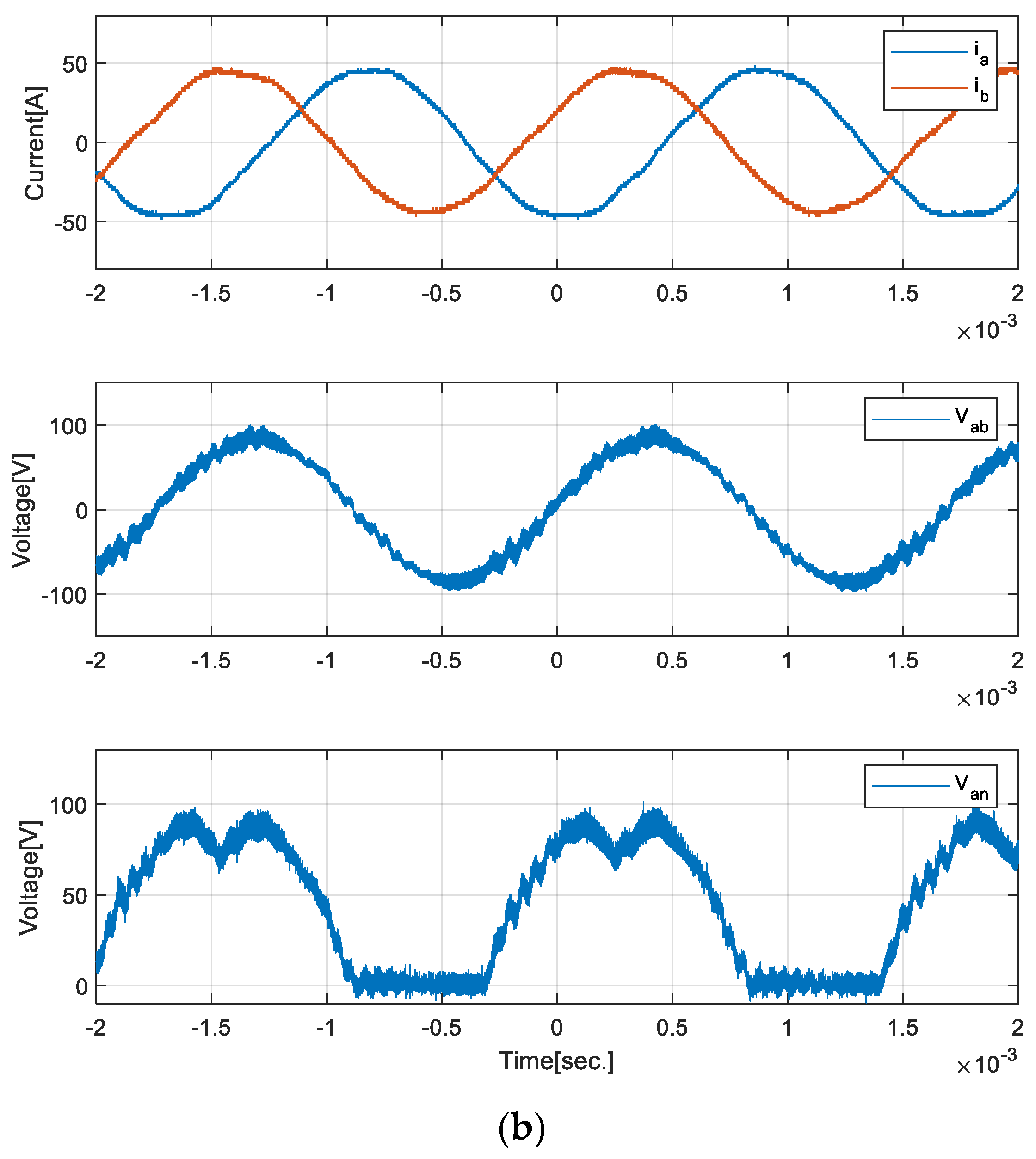
3. Hardware Implementation and Test

The hardware prototype is shown in Figure 7, together with the selected commercial control board [13]. Si MOSFETs on the low-voltage input side are Infineon IPT020N10N3, and SiC MOSFETs on the high-voltage output side are ROHM SCT3017ALHR. Input and output cells are switched with different frequencies, 50 and 150 kHz, respectively, to optimize efficiency. Moreover, to meet power rating requirements, the inverter is implemented by interleaved cells, with a 180 deg phase-shift operation between them [6].
The selected control platform has its own software design kit, which can be installed as a toolbox of Matlab-Simulink for graphic programming of real-time control software. The custom functional blocks allow implementation of the desired functionalities for both simulation and actual automatic code generation. For instance, here, the designed system considered the sampling and feedback controller of a sensor at 50 kHz, while the boost-side SiC MOSFETs require the application of a PWM carrier of 150 kHz. As shown in Figure 8, Clock_0 was designed to be 50 kHz, and Clock_1 was set to 150 kHz. Each specific setting can be found in Figure 5 and Figure 6.
Using the two PWM reference clocks and the carrier-based PWM (CBPWM) function provided by the toolbox, dual switching frequency modulation implementation is straightforward. As the switch of each leg controls the top, and the switch of the bottom needs to consider the dead time, the output mode of the CB-PWM is simply set to Dual (PWM_H + PWM_L); the dead time can also be set by the user, with a value of 200 ns chosen in this case. In addition, as the designed hardware has two parallel power electronic cells for high current input and output, a phase parameter of the CB-PWM can be set to 0 and 0.5 to implement PWM signals with the required 180 degree phase shift.
The required duty-cycle can be implemented by the modulation method described in Section 2.2. Figure 9a shows the toolbox implementation of the three-phase target voltage (Vabc), the vector magnitude of the target voltage (Vpk), the PWM mode (if the value is 0, it calculates the duty for the sinusoidal PWM; in other cases, it generates the duty of the DPWM), and the input voltage magnitude (Vdc) to calculate the duty required for each phase. This configured subsystem is connected to the command voltage (Vaq) and the PWM function, as illustrated in Figure 9b.
Figure 10a shows real-time simulation results of the implemented interleaved carrier signals, while Figure 10b shows real-time simulated output capacitor voltage (top), cross-coupled inductor currents (center), and effective magnetizing current (bottom) for the implemented operation. The results in Figure 10 were obtained with a real-time simulation box [14], for which an interface with the control platform is readily available, also allowing for ease of use in hardware-in-the-loop (HIL) type experiments.
Controller design validation was carried out by means of DC current step response, discussed with the help of Figure 11: in (a), using a conventional controller, the target value was reached in approximately 20 ms; in contrast, employing active damping results in (b), the target value was attained within about 3 ms, a significant improvement (in these tests, the bandwidth cut-off frequency was set at 300 Hz). Based on the above preliminary results, the overall system dynamic performance was assessed using a test light-load motor before its application to the Halbach motor. Figure 12 shows representative results: in (a), the startup performance was validated, and the boosting function with an output voltage surpassing the input voltage was confirmed at maximum speed operation in (b); in (c), bidirectional power transfer capability of the Y-inverter is shown, confirming the current controller’s performance during regenerative braking.
The Halbach motor experimental setup shown in Figure 13 was assembled and used for final characterization.
Figure 14 shows representative waveforms for DPWM, with test conditions of 15.3 N-m torque and motor rotational speeds of 600 rpm and 1800 rpm in (a) and (b), respectively. Under the same load torque, motor terminal currents were approximately 30 amps at different speed conditions, while the phase-to-phase motor voltage was close to an ideal sinusoidal waveform.
Figure 15 reports the results of measured inverter efficiency for other torque and speed conditions. These results include gate-driver losses of around 12 W. The maximum efficiency measured here, for power levels up to about 50% of the maximum rating, was 97%, and it is worth noting how even partial load conditions were characterized by relatively high efficiency.
Finally, Figure 16 shows the measured harmonic distortion using the phase-to-phase motor terminal voltages and motor currents under different speed and load torque conditions: both voltage and current total harmonic distortions were below 5% at all test conditions. Such good results were due not only to the inverter, but also to the Halbach rotor machine design. Some tests carried out with a non-permanent magnet-type machine yielded different harmonic signatures. Details of the Halbach machine’s structure and design can be found in [15,16].

4. Discussion and Conclusions

Results presented demonstrate the suitability of modern control platforms and dedicated functional blocks-based SDK packages to implement real-application control solutions, even for high-frequency switching original inverter topologies and machine structures used in modern traction drives requiring regenerative braking capability. Not shown here explicitly, the same platform and approach were also used to design input and output over-voltage and over-current protections, as well as temperature monitoring and over-temperature shutdown, and their validity was confirmed experimentally in a number of dedicated tests. Definitely a powerful option for research and development laboratory environments, the time-saving opportunities offered by such an approach over alternative solutions requiring explicit programming well compensate the hardware platform cost and could also be used for commercial product delivery.

Author Contributions

Formal analysis, Y.L.; Investigation, Y.L.; Resources, A.C.; Writing—original draft, Y.L. and A.C.; Supervision, A.C.; Project administration, S.D.; Funding acquisition, A.C. All authors have read and agreed to the published version of the manuscript.

Funding

This research received support from the Discretional Presidential Grant of Kyoto University of Advanced Science and Grant 20H02138 of the Japanese Society for the Promotion of Sciences (JSPS Kakenhi Kiban B).

Data Availability Statement

Data are contained within the article.

Conflicts of Interest

The authors declare no conflicts of interest.

References

  1. Husain, I.; Ozpineci, B.; Islam, M.S.; Gurpinar, E.; Su, G.J.; Yu, W.; Chowdhury, S.; Xue, L.; Rahman, D.; Sahu, R. Electric drive technology trends, challenges, and opportunities for future electric vehicles. Proc. IEEE 2021, 109, 1039–1059. [Google Scholar] [CrossRef]
  2. Antivachis, M.; Bortis, D.; Schrittwieser, L.; Kolar, J.W. Three-phase buck-boost Y-inverter with wide DC input voltage range. In Proceedings of the 2018 IEEE Applied Power Electronics Conference and Exposition (APEC), San Antonio, TX, USA, 4–8 March 2018; pp. 1492–1499. [Google Scholar]
  3. Melo, V.; Melo, A.; Santos, W.; Fardin, J.; Encarnação, L. Open-loop single-phase space state model and equivalent circuit of a non-conventional three-phase inverter. Electronics 2020, 9, 744. [Google Scholar] [CrossRef]
  4. Endo, Y.; Jaber, H.J.; Minami, M.; Castellazzi, A. Floating output series interleaved boost-only GaN Y-Inverter. In Proceedings of the 2022 25th International Conference on Electrical Machines and Systems (ICEMS), Chiang Mai, Thailand, 29 November–2 December 2022; pp. 1–4. [Google Scholar]
  5. Jaber, H.J.; Castellazzi, A. Frequency and Modulation Index Related Effects in Continuous and Discontinuous Modulated Y-Inverter for Motor-Drive Applications. In Proceedings of the 2022 24th European Conference on Power Electronics and Applications (EPE’22 ECCE Europe), Hanover, Germany, 5–9 September 2022; pp. 1–8. [Google Scholar]
  6. Jaber, H.J.; Horie, K.; Domae, S.; Castellazzi, A. Dual switching-frequency hybrid Si-SiC Y-Inverter. In Proceedings of the 2023 11th International Conference on Power Electronics and ECCE Asia (ICPE 2023-ECCE Asia), Jeju Island, Republic of Korea, 22–25 May 2023; pp. 757–763. [Google Scholar]
  7. Antivachis, M.; Bortis, D.; Menzi, D.; Kolar, J.W. Comparative evaluation of Y-inverter against three-phase two-stage buck-boost DC-AC converter systems. In Proceedings of the 2018 International Power Electronics Conference (IPEC-Niigata 2018-ECCE Asia), Niigata, Japan, 20–24 May 2018; pp. 181–189. [Google Scholar]
  8. Kolar, J.W.; Huber, J. Next-generation SiC/GaN three-phase variable-speed drive inverter concepts. In Proceedings of the PCIM Europe Digital Days 2021, International Exhibition and Conference for Power Electronics, Intelligent Motion, Renewable Energy and Energy Management, Online, 3–7 May 2021; VDE: Frankfurt am Main, Germany; pp. 1–5. [Google Scholar]
  9. Trang, H.; Castellazzi, A.; Domae, S.; Dong, T.; Nakamura, T. Light electric vehicle motor-drive design based on hybrid Si/SiC Y-inverter and dual-rotor Halbach machine. J. Electr. Eng. Technol. 2023, 18, 367–376. [Google Scholar] [CrossRef]
  10. Endo, Y.; Minami, M.; Jaber, H.J.; Castellazzi, A. Experimental study of interleaved Y-Inverter performance. In Proceedings of the 2022 24th European Conference on Power Electronics and Applications (EPE’22 ECCE Europe), Hanover, Germany, 5–9 September 2022; pp. 1–8. [Google Scholar]
  11. Hava, A.M.; Kerkman, R.J.; Lipo, T.A. A high-performance generalized discontinuous PWM algorithm. IEEE Trans. Ind. Appl. 1998, 2, 1059–1071. [Google Scholar] [CrossRef]
  12. Hava, A.M.; Çetin, N.O. A Generalized Scalar PWM Approach With Easy Implementation Features for Three-Phase, Three-Wire Voltage-Source Inverters. IEEE Trans. Power Electron. 2011, 26, 1385–1395. [Google Scholar] [CrossRef]
  13. Available online: https://imperix.com/products/control/inverter-control-board/ (accessed on 22 June 2024).
  14. Available online: https://www.plexim.com/products/rt_box (accessed on 22 June 2024).
  15. Dong, T.; Kwak, J.; Wei, L.; Castellazzi, A.; Nakamura, T. High power-density high-efficiency electric drive design with halbach-rotor pmsm and wbg-based high-frequency inverter. In Proceedings of the 2021 24th International Conference on Electrical Machines and Systems (ICEMS), Gyeongju, Republic of Korea, 31 October 2021–3 November 2021; pp. 1759–1762. [Google Scholar]
  16. Lee, Y.; Castellazzi, A.; Domae, S.; Nakamura, T. Regenerative Halbach-motor traction drive powered by an active-damping controlled interleaved Y-inverter. In Proceedings of the 2024 10th International Power Electronics and Motion Control Conference ECCE Asia (IPEMC 2024-ECCE Asia), Chengdu, China, 17–20 May 2024. [Google Scholar]
Figure 1. (a) Conceptual illustration of Y-inverter-based motor drive; (b) example of output voltage of one sinusoidally-modulated DC–DC converter cell; (c) phase-to-phase voltage in three-phase configuration.
Electronics 13 02610 g001
Figure 2. Cell circuit schematic and modulation diagram.
Electronics 13 02610 g002
Figure 3. (a) Reference output voltage of a single cell, as per Figure 2, in the case of DPWM; (b) amplitude normalized phase-to-neutral voltage waveform in a three-phase load configuration; (c) estimated relative amplitude of output-side switches currents as a function of load condition in cases of SPWM and DPWM; and (d) estimated relative amplitude of inductor and output capacitor currents as a function of load condition in cases of SPWM and DPWM.
Electronics 13 02610 g003
Figure 4. Overall control structure of interleaved buck–boost Y-inverter-fed three-phase AC motor drive system.
Electronics 13 02610 g004
Figure 5. Equivalent circuit of Y-inverter in AC motor with virtual resistor in the d-q synchronous reference frame.
Electronics 13 02610 g005
Figure 6. Block diagram of current controller with active damping and anti-windup limiter.
Electronics 13 02610 g006
Figure 7. Hardware prototype of Y-inverter, controller, and auxiliary power board.
Electronics 13 02610 g007
Figure 8. Controller clock setting for the dual switching frequency.
Electronics 13 02610 g008
Figure 9. (a) Functional block implementation of the modulation strategy; (b) overall modulation program functional implementation.
Electronics 13 02610 g009
Figure 10. Real-time simulation results of interleaved DPWM: (a) carrier signals for one cell; and (b) cell output voltage (top), inductor currents (center), and equivalent core-magnetizing current (bottom).
Electronics 13 02610 g010
Figure 11. Step response of the current controller with unbalanced interleaved power module. (a) Conventional PI control, and (b) PI control with the active damping method.
Electronics 13 02610 g011
Figure 12. Representative experimental results of motor phase-current (top), phase-to-phase voltages (center), and speed reference (bottom) in (a) startup; (b) acceleration; and (c) braking.
Electronics 13 02610 g012aElectronics 13 02610 g012b
Figure 13. Experimental setup of interleaved buck–boost Y-inverter-fed three-phase AC single-rotor Halbach motor drive system.
Electronics 13 02610 g013
Figure 14. Halbach motor terminal current (ia, ib), terminal phase-to-phase voltage (Vab), and buck–boost output capacitor voltage (Van): (a) 600 rpm (electrical 200 Hz) and 15.3 N-m load torque condition results; and (b) 1800 rpm (electrical 600 Hz) and 15.3 N-m results.
Electronics 13 02610 g014aElectronics 13 02610 g014b
Figure 15. Inverter efficiency in the motor test bench with Halbach motor at various load–torque conditions.
Electronics 13 02610 g015
Figure 16. Measured total harmonic distortion under various load–torque conditions: (a) voltage THD; and (b) current THD.
Electronics 13 02610 g016
Disclaimer/Publisher’s Note: The statements, opinions and data contained in all publications are solely those of the individual author(s) and contributor(s) and not of MDPI and/or the editor(s). MDPI and/or the editor(s) disclaim responsibility for any injury to people or property resulting from any ideas, methods, instructions or products referred to in the content.

