1. Introduction
Quantum computing represents a revolutionary paradigm of computability aimed at exploiting quantum algorithms, which are based on quantum mechanical phenomena, such as the superposition of states and entanglement, to solve problems not efficiently addressable with classical algorithms [
1,
2,
3]. The most promising problems of practical interest are mathematically demanding, involve small datasets, and allow for the solving of quantum algorithms with exponential speed-up [
4]. Prime number factorization, which is efficiently performed by quantum Shor’s algorithm in a polynomial time [
5], is a historical example of such a class of mathematical problems. To preserve their speed-up, quantum algorithms should run on a quantum microprocessor that essentially is an array of quantum bits, or qubits for short. During the execution of a quantum algorithm, qubits are entangled and/or manipulated to form quantum gates, which are the elementary bricks of the quantum processor. Entanglement also allows for the formation of logic qubits, which are useful for minimizing errors [
6].
Any two-state quantum physical system, whether intrinsic, a subset, or engineered, can encode a qubit [
3,
6]. Several solid-state technologies are available for implementing a qubit, with superconducting qubits being the most widely adopted nowadays. The spin and charge of an electron confined in a Quantum Dot (QD) may also be exploited to manufacture a solid-state qubit. Historically, the single electron spin was the first contemplated option for quantum computation [
7]. Today, QD-based qubits remain promising candidates by virtue of their scalability, small footprint, long coherence time, and compatibility with Complementary Metal-Oxide-Semiconductor (CMOS) microelectronic technology [
8,
9,
10,
11].
Microwave pulses enable the manipulation of superconducting and electron spin qubits. The frequency of the microwave pulse should match the resonance frequency
(
) of the wanted quantum transition corresponding to the quantum gate to reproduce [
12]. A common approach, widely adopted in research laboratories, involves generating microwave pulses using rack-mount instrumentation operating at room temperature. However, since a qubit must operate at deep-cryogenic temperatures (10 Mk–4 K) to preserve its quantum peculiarity, these pulses are then transmitted to the qubits via microwave cables [
13]. Regrettably, the cables are not only bulky, but they also convey a considerable amount of heat into the cryostat hosting the qubits. Sustaining cryogenic temperatures under such circumstances may prove challenging. These difficulties and limitations pose significant hurdles, especially considering that the targeted number of qubits for the next decade is in the range of 100,000 [
14].
Miniaturized microwave sources, tailored as cryogenic integrated circuits, appear to be very promising for the fabrication of solid-state quantum microprocessors. They can indeed be placed close to the qubits, thus alleviating, if not entirely avoiding, the aforementioned issues. The ultimate goal is the integration of the qubits along with the control and read-out circuitry on the same silicon die. The actual state-of-the-art envisages a chipset consisting of the quantum chip carrying the qubits and the classical chip carrying the microwave source. Several options are possible. They can be Josephson junction-based superconducting circuits [
15,
16] or cryogenic CMOS Radio Frequency Integrated Circuits (RFICs) [
11,
17,
18]. The former allow for ultimate performance in terms of dissipated power but at the expense of a larger footprint, and the latter consumes a smaller silicon area, but they dissipate more. What makes the CMOS RFICs particularly appealing is their straightforward compatibility with the CMOS microelectronic technology. Photonics microwaves may be a further possible approach [
19]. This paper reports on a cryogenic CMOS modulator.
Regardless of the specific way of implementing the microwave sources, the microwave pulses must be applied for a precise time interval to execute a quantum gate [
12], and they undergo Amplitude Modulation (AM). A straightforward AM modulator generates a spectrum that exhibits the carrier and the Double Side Band (DSB) of the modulating envelope. Feasible as a balanced AM modulator [
20], a Double-Side Band Suppressed-Carrier (DSB-SC) modulator suppresses the carrier but not the DSB. This is not acceptable, because the modulated microwave pulse can address several resonance frequencies simultaneously, as depicted in
Figure 1. This figure shows that a Lower or Upper Single-Side Band (LSSB or USSB) modulator, whose fundamental building block diagram is shown in
Figure 2, addresses only one single resonance frequency without interfering with the others. It is worth noticing that several cryogenic microwave RFICs adopt an SSB modulation scheme [
11,
18,
21].
The mixer
M1 (
M2) receives, as inputs, the in-phase (quadrature) Local Oscillator (LO) carrier
(
) at frequency
and the Intermediate Frequency (IF) modulating signal
(
) at frequency
. A quadrature or Hilbert filter generates
from
. It is worth noting that the filter is physically feasible only with approximation, because its impulse response is an anti-causal signal [
20]. Therefore, the use of the Hilbert filter should be avoided whenever possible. For this reason, a quadrature oscillator typically generates the LO carrier. The outputs
and
of the two mixers are then algebraically summed to obtain an SSB modulated signal
.
This paper proposes a modulator, designed around a low-frequency USSB modulator and a frequency divider, for the control of two qubits. It is worth noting that one-qubit and two-qubit quantum gates form a universal set for quantum computing, with single-qubit rotations and two-qubit quantum gates being the most common [
22].
This paper is organized as follows.
Section 2 details the architecture and the mathematical analysis of the proposed modulator, along with its advantages.
Section 3,
Section 4,
Section 5 and
Section 6 address the schematics and simulations of the circuits forming the proposed modulator. The circuits were designed using Cadence Virtuoso in the SG13G2 130 nm SiGe BiCMOS technology by IHP (Innovation for High-Performance Microelectronics) in Frankfurt am Oder, Germany. In particular, the recently released cryogenic Design Kit was used. In all designed circuits, the source and body terminals of the transistors are tied together to avoid the body effect. Apart from the schematics view, this is physically feasible, because the adopted technology is triple well.
Section 7 reports on the simulations of the whole modulator. Finally,
Section 8 draws conclusions and proposes future outlooks. All simulations were carried out at 4 K. No further temperatures were addressed, because the cryostat temperature is expected to be well controlled.
2. Architecture
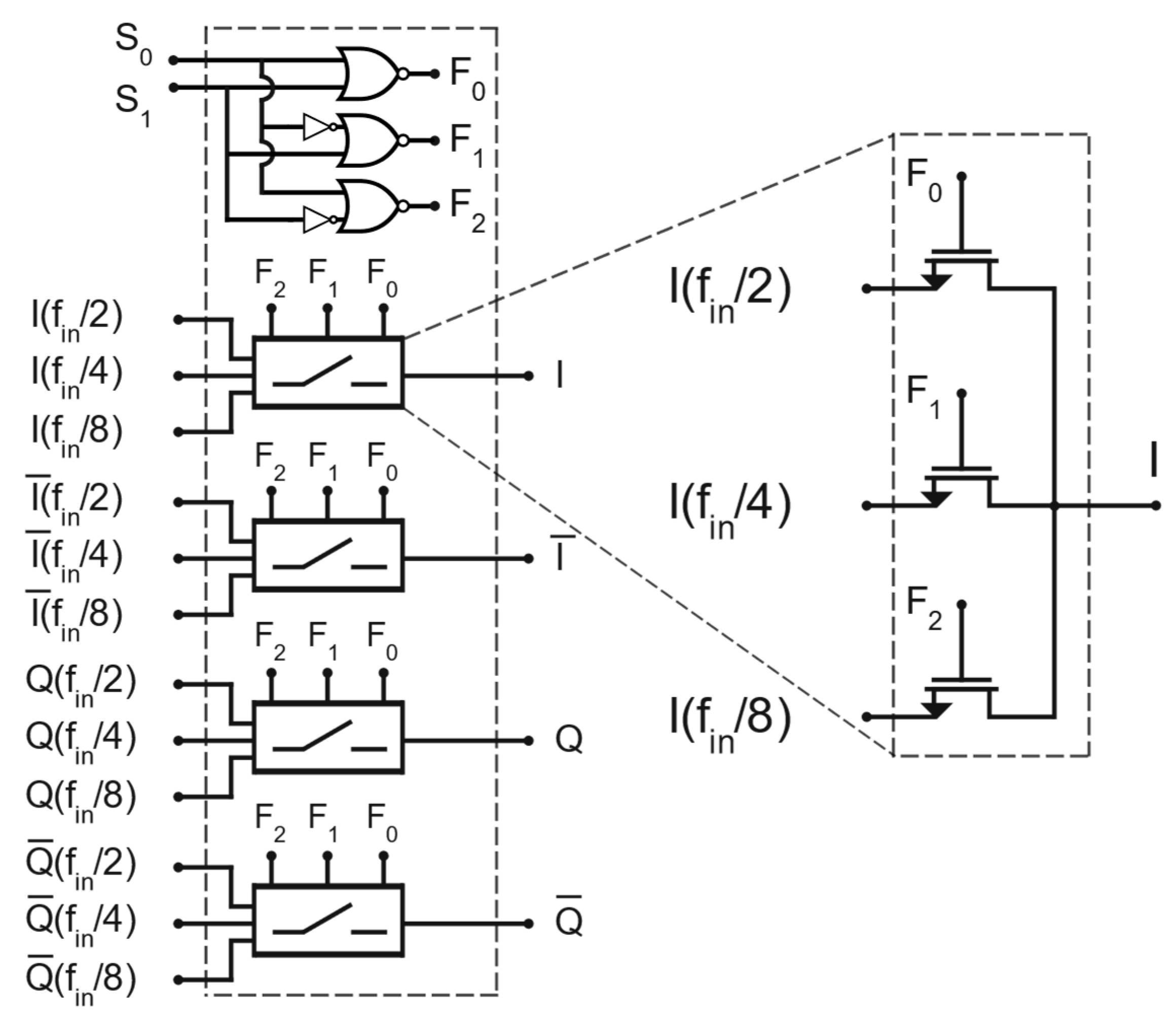
Figure 3 depicts the building block diagram of the proposed modulator. It consists of a low-frequency USSB modulator followed by the higher frequency up-conversion mixer
M3. Two IF sinusoidal tones at frequency
and
allow for the control of two qubits. There are two possible ways to generate the IF signal
, both involving amplitude modulation and the sum of signals. However, they differ in the execution order.
In Solution 1, each IF signal is first modulated and then added to the other modulated signal. Although this solution requires a modulator for each IF signal, it offers the advantage of allowing for the use of different envelopes for the two IF signals. This may be useful to minimize, by phase compensation when needed, the AC Stark shift of the resonance frequency [
21].
On the other hand, Solution 2 first adds and then collectively modulates the IF signals. This solution utilizes only one modulator, but it forces the same envelope for both signals, reducing flexibility.
For the sake of simplicity, in the following analysis, it is assumed that the modulating signals are not applied and that all the mixers behave like a Gilbert multiplier [
23,
24]. It is worth pointing out that the mixer, conceived by Howard E. Jones in 1963 [
25], and the Gilbert cell are different engines [
26]. The Gilbert cell generates only second-order intermodulation products, whereas the mixer also generates intermodulation products of higher orders. Since the SSB modulator mainly exploits second-order intermodulation products, a simplified analysis treats a mixer as a multiplier.
Let the two IF signals be
and
. This, therefore, results in the
signal to be as follows:
The
phase shifters yield the two following signals,
and
:
Equations (2) and (3) show that
and
are in quadrature, because they exhibit a relative phase shift of
. Unlike the use of a single Hilbert filter on one branch as in
Figure 2, the employment of two
phase shifters makes the architecture more symmetric.
A frequency divider, with a division ratio of
, generates the LO signals
and
in quadrature [
27] from a sinusoidal tone at frequency
. The division ratio
can be chosen to be equal to 2, 4, or 8 by selecting the output of the appropriate frequency divider by means of a multiplexer (MUX). Therefore, the LO signals
and
are as follows:
At the RF output ports of the mixers
M1 and
M2, the signals
and
are consequently the following:
where the following trigonometric identities are noted:
and
. The constant
, of physical dimension [V
−1], causes the amplitude of the signals
and
to be measured in Volt and not in Volt
2. In a real circuit, its presence is embedded in the transfer function of a real multiplier [
26].
The signal
at the output of the sum node Σ is, therefore, as follows:
where the trigonometric identity
, with
and
, is noted. It is worth pointing out that the frequency components of the two signals
and
undergo a destructive or constructive interference, as a consequence of their algebraic sum. In particular, subtracting the two signals as in Equation (8) leads to destructive interference for the components at frequencies
and
, and to constructive interference for the components at frequencies
and
. Therefore, the modulator in
Figure 3 behaves as a USSB. Vice versa, adding the signals leads to constructive interference for the components at frequencies
and
, and destructive interference for the components at frequencies
and
.
Eventually, the mixer
M3 up-converts the signal
by means of the LO tone at frequency
. The resulting RF output signal
is as follows:
where the trigonometric identity
was used once again. The output spectrum exhibits thus four different frequency components. In Equation (9), the constant
of physical dimension [V
−2] causes the amplitude of the signal
to be measured in Volt and not in Volt
3. In a real circuit, its presence is embedded in the transfer function of a real multiplier [
26].
The building block diagram in
Figure 3 has been Verilog coded within Cadence Virtuoso.
Figure 4 shows the one-sided spectra of
and
, simulated for
= 1 GHz,
= 8,
= 140 MHz,
= 240 MHz,
= 1200 mV, and
= 200 mV. Consistent with Equation (8), the spectrum exhibits two frequency components at the frequencies 1.140 GHz and 1.240 GHz, each with an amplitude of 240 mV. Similarly, in accordance with Equation (9), the signal exhibits components at the frequencies of 6.760 GHz, 6.860 GHz, 9.140 GHz, and 9.240 GHz, each with an amplitude of 144 mV. The Verilog simulations implicitly assumed the constants
to be unitary.
Table 1 below succinctly summarizes the previous comparison.
The single-step frequency conversion in the SSB modulator depicted in
Figure 2 generates second-order intermodulation products at the frequencies
. These frequencies are intended to match a qubit resonance frequency
located close to
. Typically, the frequency
is in the order of a few GHz, and
ranges from tens to hundreds of MHz. The narrow frequency separation
urges to resort to a bandpass filter of the very high-quality factor
. The practical approach involves thus interferometry at RF frequencies, at which, nevertheless, parasitic capacitances may introduce significant imbalances.
On the other hand,
Figure 3 shows that the frequency spacing between the second-order intermodulation products in the proposed modulator is
For
= 1 GHz, this spacing is large enough to accommodate a couple of qubits at the frequencies of the lower (higher) intermodulation products without taking care of the possible AC Stark effect, which the intermodulation products at higher (lower) frequencies may induce. An off-chip bandpass filter may be used to reduce the magnitude of the unused second-order intermodulation products. Since
is much lower than
, the quality factor
of the filter can be estimated to be in the order of tens of (
for the lower frequency intermodulation products and of tens of
for the higher frequency intermodulation products. It is worth noticing that the frequency divider keeps the
relaxed, because it makes
dependent on
but independent of
. In this way, the design of the filter is simpler, and it can be used to limit the potential impact of the image tone to the Spurious Free Dynamic Range (SFDR) in cases where it is desired, in spite of the fact that the second-order intermodulation products are well frequency spaced.
Moreover, the frequency divider allows for the use of only one Local Oscillator (LO). In
Figure 3, the LO is assumed to be off-chip. The use of one single LO simplifies the experimental set-up. In cases where the LO is on-chip, it would take the form of a Phase Locked Loop (PLL), which is a complex circuit. The use of one single LO would save the silicon area and reduce power dissipation.
The frequency divider offers the further advantage of avoiding the use of a Hilbert filter or of a quadrature oscillator, because the divide-by-2 frequency dividers generate the in-phase and quadrature tones necessary for the USSB modulator [
27].
In summary, the frequency divider offers several advantages. Firstly, it reduces the necessity for a bandpass filter, making it less essential. Moreover, should a bandpass filter be desired, the frequency divider alleviates the constraints on its quality factor. Additionally, the frequency divider reduces the requirement for frequency synthesis to just a single PLL, and it eliminates the need for Hilbert filters or quadrature oscillators.
3. Polyphase Filter
The ±
π/4 phase shifters in
Figure 3 were designed as a Polyphase Filter (PPF), whose schematic is depicted in
Figure 5.
It is the cascade of two double-stage, type II PFFs [
28]. By assuming periodic signals, the first filter produces a
dephased couple of differential signals from the single input differential signal applied at the input nodes
and
. In this way, the four-output single-ended signals split the full
angle into four phases, which is the reason why the filter is dubbed four-phase. The principle can be extended to a
-phase PPF, which receives
input differential signals and returns
output differential signals, which are
single-ended signals. Following this, the second filter is an eight-phase PPF, because it receives two differential signals from the first PPF, and it generates four output differential signals, splitting the
angle into eight phases. Each filter was designed to be two-stage ones, in order to enlarge the bandwidth [
28]. By keeping
, the capacitance of the capacitor
(
) was chosen, such that
(
), with
(
) being the lower (higher) cut-off frequency of the filter. For minimum phase errors, the capacitance of the capacitor
(
) was chosen, such that
(
) is the geometric mean of
and
(
and
) [
28], so that
from which the following is derived:
Since the frequencies of the IF signals are 140 MHz and 240 MHz, the PPF was designed with = 100 MHz and = 300 MHz. The obtained capacitances, calculated for = 1 kΩ, are = 1.60 pF ( = 625 Mrad/s), = 1.11 pF ( = 900 Mrad/s), = 0.77 pF ( = 1299 Mrad/s), and = 0.53 pF ( = 1887 Mrad/s).
Figure 6a shows the simulated phases of the eight single-ended voltage signals
(
= 1…8) at the output of the PPF. At
= 100 MHz, the values match with the desired phases reported in
Figure 5. For higher frequencies, the phases roll off, but what is most important is that the relative phase is kept constant.
Figure 6b plots the ratio between the amplitude of each output single-ended signal
and the amplitude of the differential input signal of the PPF. This figure shows that the four used
signals exhibit the same amplitude even if not constant over the bandwidth. Some amount of splitting in the curves has to be expected, because of the approximated physical feasibility of a Hilbert filter. By means of a phasorial picture,
Figure 7 shows that, in accordance with the architecture in
Figure 3, only the even phases were used; in particular, the signals
and
were used to obtain the differential signal
and the signals
and
to obtain the differential signal
. It is worth noting that varactors may make the polyphaser filters tunable to compensate for some unbalances [
29]. Nevertheless, since the used Design Kit is a cryogenic one and the polyphaser filter operates at low frequencies, the filter was tailored as a fixed RC network.
5. Design of the Low-Frequency Mixer
Figure 13 depicts the schematic of the mixers
and
used for the USSB in
Figure 3. The transistors
and
form the transconductance stage and operate under small-signal conditions. They convert the Intermediate Frequency (IF) voltage signals, applied to their gates, into IF small-signal currents
, where
and
are, respectively, the transconductance and the small-signal gate–source voltage of the transistors
and
, with
and
. The transistors
−
constitute the switching stage. To this aim, the LO signal must be sufficiently large to make these transistors behave as switches. In this way, they invert the polarity of the IF currents at the LO frequency rate, enabling frequency conversion by time variance.
The switching activity generates small-signal currents with an RF spectrum reach of intermodulation products at the frequency
, where
and
are integer numbers, resulting from the two input tones at the frequencies
and
. They can be addressed by means of the short-circuit currents
at the output nodes
and
. By assuming that the input IF voltage signals on the gates of
and
are cosinusoidal tones of the amplitude
and the frequency
and are in phase opposition, you can write the following:
where
is a periodic square wave oscillating between
and
at the frequency
. It describes the periodic inversion polarity of the current due to the switching activity. The expansion of
in its Fourier series yields the following:
which can be rewritten as follows:
where Werner’s trigonometric identity
is noted. The approximation of a mixer with a multiplier, under which only the second-order intermodulation products are of interest (see
Section 2), leads to the following simplified mathematical expression of
:
By supposing that the transistors
−
switch ideally, and by neglecting the capacitive parasitics, the Driving Point Impedance (DPI) technique [
34] calculates the RF small-signal output differential voltage
as
by the differential output resistance
:
Since the amplitude of the IF input differential voltage signal
is equal to
, Equation (24) yields the voltage conversion gain of the mixer equal to
, in agreement with [
35]. On the other hand, if the transistors
−
do not switch ideally and/or capacitive parasitics should be accounted for, it is more efficient to analyze the circuit in the frequency domain. From Equation (23), the one-sided spectrum
of
is as follows:
where
is the Dirac’s delta function. The spectrum
exhibits, therefore, two lines of the magnitude
. After the DPI technique, the one-sided spectrum
of
is as follows:
where
is the differential output impedance.
Figure 3 shows the adopted sizing of the transistors and resistors. The bias DC gate voltage for
and
was set to 850 mV. With that sizing, the transistors
and
are biased in the saturation region with
= 7.725 mS.
The mixer was simulated for
= 1 mV and
= 10 MHz and for an LO square wave oscillating between 0 and 1.7 V at a frequency of
= 1 GHz. For these amplitudes, the transistors
and
are in the saturation region all the time, so they operate as class A transconductors, while the transistors
−
are in the saturation region under DC conditions, nay for the mean value of the clock, in the triode region when the clock is high and in the off state when the clock is low.
Figure 14a depicts the obtained one-sided spectrum. As expected from Equation (25), the spectrum exhibits two lines with the same magnitude and at the frequencies of 1010 MHz and 990 MHz. In particular, the value of the magnitude is also in agreement with Equation (25). Given
= 7.725 mS and
= 1 mV, the resultant calculation yields
= 4.92 μA.
The differential output impedance
was simulated by means of the Periodic Scattering Parameter (PSP) simulation, with the square waveform large signal LO setting the time variance rate of the circuit. The modulus of
was found to be equal to 1.42 kΩ at 990 MHz and 1.40 kΩ at 1010 MHz. In good agreement with the simulated spectrum
in
Figure 14b, Equation (26) indeed yields a magnitude of about 7.00 mV for the line at 990 MHz and of 6.89mV for the line at 1010 MHz. The error between simulations and calculation is about 8%.
Table 3 below collects and compares the amplitudes discussed above.
Figure 15 shows that the node Σ in the USSB modulator in
Figure 3 was obtained by appropriately combining the RF currents generated by the couple of mixers. In particular, the positive phase current coming out from one mixer was combined with the negative phase current coming out from the other mixer. Since the two mixers share the same differential resistive loads, the DC current flowing through the load resistors in
Figure 15 is two times the DC current flowing through the load resistors in
Figure 13. The load resistors for the double mixer were thus sized as half of the load resistors for the single mixer to keep the same DC operating point used for the single mixer.
By means of the same analysis approach used for the single mixer in
Figure 13, it is straightforwardly demonstrated (see
Appendix A) that, for the mixer in
Figure 15, the mathematical expression of the second-order intermodulation component of the output short-circuit current is as follows:
Equation (27) shows that the one-sided spectrum
of the short current
is a single line at the frequency
and of magnitude
. It is worth noticing that this magnitude is two times the magnitude of the
of the single mixer in Equation (23). This stems from the fact that the short-circuit currents of the double mixer result from the constructive interference of two short-circuit currents.
Figure 16a depicts the one-sided spectrum of the output short-circuit current simulated under the same conditions used for the single mixer, that is
= 1 mV,
= 1 GHz, and
= 10 MHz. Since the transconductances of the transconductor transistors are the same for the two mixers, that is
= 7.725 mS, and because the single and double mixers were designed to have the same bias point, the simulated magnitude agrees with Equation (27), which yields
= 9.84 μA. The magnitude of the one-sided spectrum of the output differential voltage was calculated by means of the DPI. The PSP simulations yielded the modulus of
, which is equal to 727.4 Ω at 1010 MHz. In agreement, within an error of about 9%, with the simulated spectrum
in
Figure 16b, the DPI yields a magnitude of 7.16 mV for the magnitude of
at 1010 MHz.
Table 4 summarizes these calculated and simulated amplitudes.
6. Design of the High-Frequency Mixer
Figure 17 depicts the schematic of the up-conversion mixer
M3. It is the same mixer in
Figure 13, apart from the two RC bias networks for the transistors
and
. The resistance and capacitance are, respectively, 6 kΩ and 2 pF. The supply voltage
, tail current
, and DC gate bias for
M1 and
M2 are the same as those adopted for the mixer in
Figure 13.
Figure 18 depicts the one-sided spectrum of the short-circuit current simulated for
= 1 mV and
= 1 GHz and for an LO square wave oscillating between 0 and 1.7 V at a frequency
= 8 GHz. Apart from the higher
and
, these are the same conditions used for the simulation of the mixer in
Figure 13. It is also worth noting that
= 8 GHz corresponds to
= 8 in the architecture depicted in
Figure 3. The spectrum exhibits two lines with the same magnitude of about 4.87 μA, in agreement with Equation (25), within a discrepancy of 1%, which yields 4.92 μA for
= 7.725 mS and
= 1 mV.
Once again, the one-sided spectrum of the differential output voltage was calculated by means of the DPI technique. The PSP simulations yielded a modulus of the differential output impedance of 318 Ω (240 Ω) at the frequency of 7 GHz (9 GHz), corresponding to a magnitude of , which is equal to 1.57 mV (1.18 mV), in agreement with the simulated magnitude of 1.69 mV (1.36 mV), within a discrepancy of about 7% (13%).
Table 5 below collects and compares the amplitudes discussed above.
7. Simulation of the Modulator
This section addresses the transistor-level simulation of the modulator whose architecture is depicted in
Figure 3. The two input IF differential signals are two sinusoidal tones of amplitude 10 mV and frequencies 140 MHz and 240 MHz. The LO differential signal was a square wave of amplitude 1.7 V.
Figure 19 shows the spectrum of the output differential signal generated by the modulator when the division ratio
= 8, that is when the LO frequency
is 8 GHz. The spectrum exhibits four tones at the frequencies of 6.76 GHz, 6.86 GHz, 9.14 GHz, and 9.24 GHz, in agreement with the Verilog simulation in
Figure 4b.
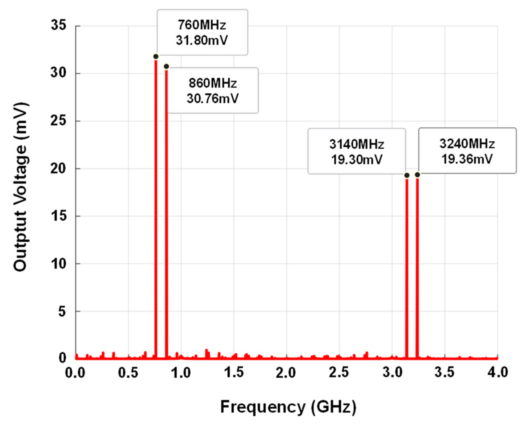
Figure 20 and
Figure 21 also demonstrate the same agreement between circuit-level and Verilog simulations for
= 4 (
= 4 GHz) and
= 2 (
= 2 GHz), respectively.
An assessment of the correctness of the amplitudes needs the evaluation of the voltage conversion gain of the mixers at the frequencies of interest. For the mixer in
Figure 15, it is necessary to determine the voltage conversion gain for the output frequencies of 1140 MHz and 1240 MHz. In this case, the mixer cannot be simulated on its own as in
Section 5 because of the loading effect due to the up-conversion mixer. The simulations showed a voltage conversion gain of approximately 3.1, which is lower than the gain deduced from
Figure 16, as expected.
On the other hand, the conversion gain of the up-conversion mixer in
Figure 17 can be calculated following the same approach used in
Section 6, because the mixer was not closed on an output load. The conversion gain was calculated for each of the twelve frequencies addressed in
Figure 19,
Figure 20 and
Figure 21. For instance, for the frequencies in
Figure 20, the following moduli for the differential output impedances were obtained from the PSP simulations: 507.6 Ω at 2760 MHz, 502.5 Ω at 2860 MHz, 323.7 Ω at 5140 MHz, and 316.5 Ω at 5240 MHz. The resulting calculated voltage conversion gain is about 1.24 at 2760 MHz and 2860 MHz and about 0.80 at 5140 MHz and 5240 MHz. For the other frequencies, a voltage conversion gain of 2.18 for the frequency couple 760 MHz and 860 MHz was found, of 1.12 for the couple 3140 MHz and 3240 MHz, of 0.80 for the couple 6760 MHz and 6860 MHz, and of 0.58 for the couple 9140 MHz and 9240 MHz.
Figure 22 summarizes these voltage conversion gains.
By means of the rough representation of the modulator in
Figure 22, it is possible to calculate the amplitudes of the lines in the spectra in
Figure 19,
Figure 20 and
Figure 21. Note that after
Figure 6b, the PPF exhibits an attenuation of about 0.5, because all the signals in
Figure 22 are differential. It is worth noting that plots in
Figure 6b are indeed the attenuation for each single-ended signal
(
= 1…8) with respect to the input differential signal.
Since the input signal exhibits a differential amplitude of 10 mV,
Figure 22 yields a differential amplitude of the lines around 5 GHz, that is at 5140 MHz and 5240 MHz, of 12.4 mV, which matches with the spectrum in
Figure 20, within an error of about 10%. For the lines around 1 GHz, that is at 760 MHz and 860 MHz,
Figure 22 yields a differential amplitude of 33.8 mV, which agrees with the spectrum in
Figure 21, within an error of about 7%. For the lines around 9 GHz, that is at 9140 MHz and 9240 MHz,
Figure 22 yields a differential amplitude of 9.0 mV, in agreement with the spectrum in
Figure 19, within an error of about 3%. For the lines around 3 GHz, the agreement remains acceptable within an error margin of 10%, whereas for the lines around 7 GHz, the error margin is 20%.
Table 6 below summarizes the above comparison.
The linearity of the modulator was assessed by means of transient simulations. A first set of simulations was carried out for
= 4 and for a single 140 MHz input IF sinusoidal tone, whose differential amplitude spanned from 10 mV to 100 mV. The picked-up differential output signal was the tone at the 2.86 GHz frequency (see
Figure 20). The voltage gain was plotted versus the differential amplitude of the IF input signal.
Table 7 collects the obtained results. It shows that a decrease of 1 dB in the voltage gain occurs for a voltage input of 80 mV. The 1 dB compression point thus corresponds to an input differential voltage amplitude of about 80 mV.
A second set of simulations were carried out for
N = 4 and for a couple of input IF sinusoidal tones at the frequency of 140 MHz and 240 MHz and with the same magnitude of 10 mV. The highest output intermodulation component was found at 2.96 GHz, with a negligible amplitude of about 0.5 μV, in agreement with
Figure 20. It is worth noting that, in the literature, the pulse amplitude at the port of a qubit driver is estimated to be in the range of a few mVs [
36].
The proposed modulator dissipates about 100 mW, which is entirely ascribed to the frequency divider. On the other hand, the two mixers dissipated about 5 mW. Even if it were improved, the power dissipation is compatible with the power budget of 1 W estimated for a cryostat working at 4 K [
36] and in the same order of magnitude of the dissipated power claimed in [
17,
18,
37,
38], as reported in
Table 8. The 2 mW power dissipation claimed in [
36] for a 28 nm bulk-CMOS cryo-controller remains outstanding. It is worth noticing that the adopted mixers are passive.
The low- frequency SSB mixer sets the noise figure of the modulator to about 23 dB, which should mainly be ascribed to the input PPF, whose simulated minimum noise figure is about 13 dB, a value in agreement with the following formula [
39]:
which provides the minimum noise figure for an
N layer polyphaser filter. Equation (28) yields
= 16 dB for
= 4. The up-conversion mixer exhibits a DSB NF of about 5 dB. Since the noise figure of transmitters are not usually reported in the literature, it may be useful to cite the noise figure of 20–25 dB for the 180 nm CMOS 5 GHz quadrature down-converter described in [
40], which shares, with the proposed modulator, mixers similar to the mixer in
Figure 3 and a PPF in the input signal path.
Eventually,
Table 8 below helps to compare the proposed modulator with other qubit controllers in the literature. The Multi Project Wafer (MPW) costs are those available on the websites of the IC services Europractice (Europe) and CMC Microsystems (Canada). Only this paper and [
41] keep a cost low by using bulk CMOS. All the other implementations exhibit higher MPW costs because of the adopted FinFET technology.
Table 8.
Comparison summary.
Table 8.
Comparison summary.
| | This
Work | [17] | [18] | [36] | [37] | [38] | [41] | [42] |
|---|
Operating
temperature
[K] | 4 | 3 | 3 | 3 | 3 | 4 | 3.5 | 3 |
Qubit
technology | Spin and
Trans. | Spin | Spin and
Trans. | Trans. | Spin and
Trans. | Spin | Trans. | Trans. |
Dissipated
power
[mW] | 100 | 360 | 384 | 2 | 384 | 190 | 12 | 23 |
Frequency
range
[GHz] | 0.9–9 | 2–20 | 5–20 | 4–8 | 2–20 | 11–17 | 4.6–8.1 | 4.5–5.5 |
Number
of qubits | 2 | 32 | 32 | 1 | 2 | 16 | 1 | 1 |
IF signal
source | Off-chip | On-chip | On-chip | On-chip | On-chip | On-chip | On-chip | On-chip |
LO signal
source | Off-chip | Off-chip | Off-chip | Off-chip | Off-chip | Off-chip | Off-chip | Off-chip |
CMOS
technology | 130 nm
bulk | 22 nm
FinFET | 22 nm
FinFET | 28 nm
bulk | 22 nm
FinFET | 22 nm
FinFET | 40 nm
bulk | 14 nm
FinFET |
MPW cost
[kEUR/mm2] | 7.3 | 27.2 | 27.2 | 14 | 27.2 | 27.2 | 6.1 | 14.7 |
8. Conclusions
This paper reported on the design of a modulator aimed to control 2 qubits. The circuit was tailored as an RFIC and designed by using the cryogenic Design Kit of SG13G2 130 nm SiGe BiCMOS technology by the IHP foundry (Innovation for High-Performance Microelectronics) in Frankfurt am Oder, Germany.
A low-frequency Upper Single-Side Band (USSB) modulator and a following high-frequency up-conversion mixer form the core of the proposed modulator. An off-chip microwave source provides a large LO signal for the mixers. In particular, a frequency divider allows for the use of this external LO signal for both the low-frequency modulator and the high-frequency mixer. This is the most interesting peculiarity of the proposed modulator, because the frequency divider leads to several advantages.
It enables the carrier and its image at the output of the up-conversion mixer to be sufficiently spaced in frequency to accommodate a couple of qubits with resonance frequencies close to the carrier or its image. For instance, with reference to
Figure 20, you can address two qubits of resonance frequencies equal to 2760 MHz and 2860 MHz (5140 MHz and 5240 MHz) without taking care of the tones at higher (lower) frequencies. Nevertheless, the magnitudes of the unused tones can be reduced by introducing an off-chip band-pass filter, whose quality factor is relaxed by the use of the frequency divider. In addition, the frequency divider reduces the need for frequency synthesis to a single PLL, and it avoids the use of Hilbert filters or quadrature oscillators to generate the in-phase and in-quadrature tones for the USSB.
The frequency divider was designed to divide by 2, 4, and 8. This makes the proposed modulator a multi-frequency one, because it allows for addressing qubits, whose resonance frequencies are close to 1 GHz, 3 GHz, 5 GHz, 7 GHz, and 9 GHz. This may be useful, because each qubit technology has different resonance frequency ranges. Indeed, for Nitrogen-Vacancy qubits, the typically exploited resonance frequency is 2.87 GHz [
43]; for superconducting qubits, the resonance frequency spans between 500 MHz and 10 GHz; for trapped ion qubits, the frequency range is in the order of a few GHz; and semiconductor spin qubits cover a frequency range from hundreds of MHz to up to tens of GHz [
44].
Nevertheless, it is worth noticing that even though the modulator does not use any integrated inductor, the sensitivity curves of the frequency dividers make it narrowband. The architecture can be re-employed for addressing a different set of frequencies but at the effort of retuning the sensitivity curves of the frequency dividers, which is mainly possible by choosing the capacitor
appropriately (see
Table 2).
The agreement between the mathematical modeling, the Verilog, and the transistor-level simulations, together with the general good consistency between the transistor-level simulations of the individual building blocks (polyphase filter and the lower and higher frequency mixers) and of the whole modulator, proves that the architecture of the proposed modulator is effectively implementable in the IHP 130 nm cryogenic BiCMOS technology.
The main advantage offered by the proposed architecture is that the SSB interferometry takes place at a lower frequency with respect to other controllers claimed in the literature, where the interferometry occurs at a high frequency (see, for instance, references [
21,
36,
37]). A low-frequency interferometric structure is less sensible to gain and phase impairments due to the parasitics. This may relax the requirement for stringent IQ calibration, in contrast to [
21]. A final radiofrequency SSB signal may be obtained by adopting a classical filtering, because the frequency divider relaxes the quality factor of the filter.
The price to be paid is the power dissipated by this frequency divider, which is the main limitation of the proposed modulator. On the other hand, the estimated linearity and noise figure appear to be comparable.


