Article

Synthesized Improvement of Die Fly and Die Shift Concerning the Wafer Molding Process for Ultrafine SAW Filter FOWLP

1
School of Electronic Science and Engineering, Xiamen University, Xiamen 361005, China
2
Xiamen Sky Semiconductor Technology Co., Ltd., Xiamen 361026, China
*
Author to whom correspondence should be addressed.
Electronics 2023, 12(9), 2073; https://doi.org/10.3390/electronics12092073
Submission received: 6 March 2023 / Revised: 18 April 2023 / Accepted: 28 April 2023 / Published: 30 April 2023
(This article belongs to the Special Issue Advanced Electronic Packaging Technology)

Abstract

:
As the surface acoustic wave (SAW) filters incline to ultrafine, the failures resulting from the wafer molding process have become increasingly prominent. A methodology for coupling the mechanisms of die fly and die shift for the SAW filter miniatured with 737 μ m × 517 μ m × 200 μ m is developed for the trade-off between reliability and yields. In terms of die fly and die shift, the former occurs before the epoxy molding compound (EMC) is cured in the temperature rise period, while the latter occurs in the cooling stage after being cured. The die fly is induced by the fluid flow force in the high-temperature stage of heat compression, which is fatal for the scrap. Followed by the cooling stage, the CTE (coefficient of thermal expansion) misalignment between the die and epoxy molding compound (EMC) seriously affects the die shift and the following lithography process yields. The debonding critical energy in the mixed mode is employed to avert the die fly. Then, the die fly can be shunned by fine-tuning the die thickness, die layout, and EMC layout. A methodology to measure die shift was conducted, by which a total of 47,568 dies were embedded using compression molding. The mechanical error of the mounter and the die shift law are comprehensively leveraged, indicating that the die shift can be controlled within 50 μ m for 8-inch wafer-level packaging.

1. Introduction

With the gradually matured radio frequency (RF) front-end devices, miniaturized and integrated filters have become scarce in module design [1]. Fortunately, Fan-Out Wafer-Level Packaging (FOWLP) is the latest tailored and effective solution for foundries and integrated device manufacturers (IDMs) to update the device performance and minimize the package volume and gap between die and substrate [2]. Generally, FOWLP is an upgrade and extension of wafer level packaging (WLP), which, combined with the redistribution layers (RDL), provides higher input and output (I/O) capabilities, substrate-less package, lower thermal resistance, and lower parasitic effects [3,4]. However, numerous details about the potential crisis of LiTaO3-based SAW filters in the FOWLP remain unclear, wherein the wafer level molding process is pivotal to realize high yield [5]. For manufacture yield, the whole wafer is scrapped directly once die fly occurs (though few might happen). However, controlling the die shift within the tolerance threshold can meet the product shipment yield.
For the stacked embedded wafer level packaging (eWLP) [6], it is recommended to employ low CTE molding compound in 150 C , and robust adhesive tape to alleviate shift in compression molding. From the perspective of the thermal shrinkage and curing shrinkage, a compensation method is proposed to enable silicon die shift not exceed 40 μ m in an 8-inch wafer [7]. With the Castro–Macosko equation [8], flow dynamic resistance upsurges with the increased distance from the wafer center, compression speed, and epoxy resin viscosity. Through FLUENT [9], the die shift caused by the mold flow effect is less significant, accounting for 25%, while the CTE is a critical factor, accounting for 75%. The three-dimensional numerical method [10] is successfully applied to two kinds of embedded dies in wafer-level packaging, comparing velocity and pressure distribution for 100, 200, and 300 μ m die thickness. From the regression analysis, the relationship between die shift and die position is fitted to predict the needed compensation for the die mounter [11]. Young’s modulus is a critical factor for material properties in the molding process, and an optimization scheme is proposed based on the chip-first, face-down process [12]. Enhancing the adhesive strength is facilitated to solve the die shift problem for the silicon chip [13]. By taking COMSOL CFD to perform the 3D analysis base on the curing kinetics, the die shift induced from fluid flow increases from 5 μ m to 10 μ m . The die shift failure accounts for 1/3 of the wafer and, therefore, cannot be neglected [14]. EMC’s thermal and mechanical stress and chemical reaction shrinkages are determined to be the primary reasons for die shift in wafer molding [7]. The rules of thumb for alleviating drag force induced by molding are optimizing the initial diameter of molding compounds, increasing the thickness of molding compounds, and reducing the filling speed. Thereby, given the CTE of LiTaO3 is five times that of Si, the amelioration of ultrafine SAW filter die fly and shift is urgent to explore.
In addition, all these aforementioned debonding controls merely refer to the critical shear stress [15], while the standard test for complete debonding is the critical fracture energy density. Thus, this paper simultaneously employs the crack energies benchmarked with the critical debonding point. Defects are predicted by using curing kinetics to provide an accurate 3D model for the mold flow analysis. A typical obstacle in the numerical analysis of debonding phenomena is the need for extensive computational resources and prolonged solution times. Namely, the Virtual Crack Closure Technique (VCCT) and the Cohesive Zone Material Model (CZM) are typically used in commercial finite element analysis (FEA) software to analyze such problems. VCCT needs to define complex interface properties, while CZM is easier to implement. This paper focuses on the effect of stress and strain on localization near the debonding plane or the relationship of elastic energy to debonding. Solid mechanics and polymer physics are elucidated through micromechanical experiments to explain the debonding mechanisms. Generally, the root of die shift and fly is the flow-induced press force and the mechanical stress caused by a mismatch of the CTE among the packaging components. The current state of the art on how the microdies detached from the adhesive tape is analyzed. Besides the maximum stress, the deboning is correlated with the crack energy. The contributions of the present paper are fourfold as follows.
  • The pressure–volume–temperature (P-V-T) equation considering cavity vacuum is proposed to describe the internal mechanism of the volume change of epoxy molding materials. It not only achieves lower costs but also increases the yields per wafer.
  • The model focuses on the die fly caused by the mold flow, which benefits the die shift control. Based on the proposed theory, simulation and experiments quantitatively characterized two molding materials. Given the effects on die fly and shift, an optimization scheme is developed to adapt advanced IC packaging.
  • Most importantly, we also determined that the molding material’s thermal shrinkage and curing shrinkage in the spiral dispensing mode are the main reasons for the mold shift during wafer molding. From the precompensation method, it can make the die shift less than 50 μ m , and the mold area/package area ratio has a fatal effect on the die shift value.
  • By varying the die thickness, die layout, and top mold compression speed, parametric studies are conducted to discuss their effect on die fly and shift.
The remainder of the paper is structured as follows. Section 2 illustrates the thermal compression molding process of the SAW filters as the critical step of the FOWLP. Section 3 delves into the mechanism of the die fly and shift. Section 4 presents the simulation and experimental results of the die fly. Furthermore, the rule and optimization for the die shift are elucidated in Section 5. Finally, Section 6 gives the conclusions.

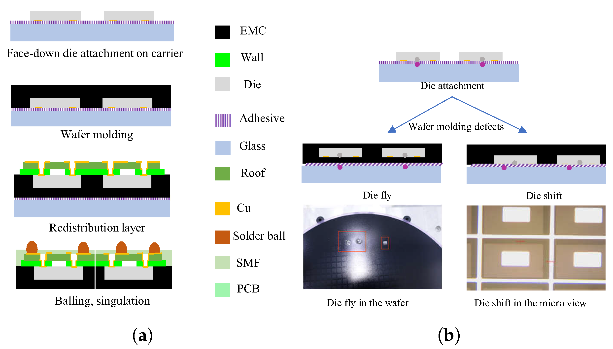
2. Thermal Compression Molding Process

Xiamen Sky Semiconductor Technology Co., Ltd. has recently introduced a novel wafer-level fan-out package for SAW filters in Figure 1, which is suitable for the microdies’ FOWLP. In Figure 1a, the cavity is formed by two passivation layers, resembling a wall and roof built for the enclosed hollow structure. Besides, the solder mask film (SMF) is formed to resist the reflow thermal shock in the solder ball assembly. From Figure 1b, in terms of die fly and die shift, we assume one is detached with the carrier by the permeability of flow EMC, while another is horizontally slid along the contact plane by the thermal strain from EMC. The key process is wafer molding, illustrated in Figure 2.
  • The support carrier is attached with a heat-foaming double-adhesive tape, as shown in Figure 3. After the liner peeling, the foaming adhesive is in contact with a glass carrier, while the base adhesive in contact with dies.
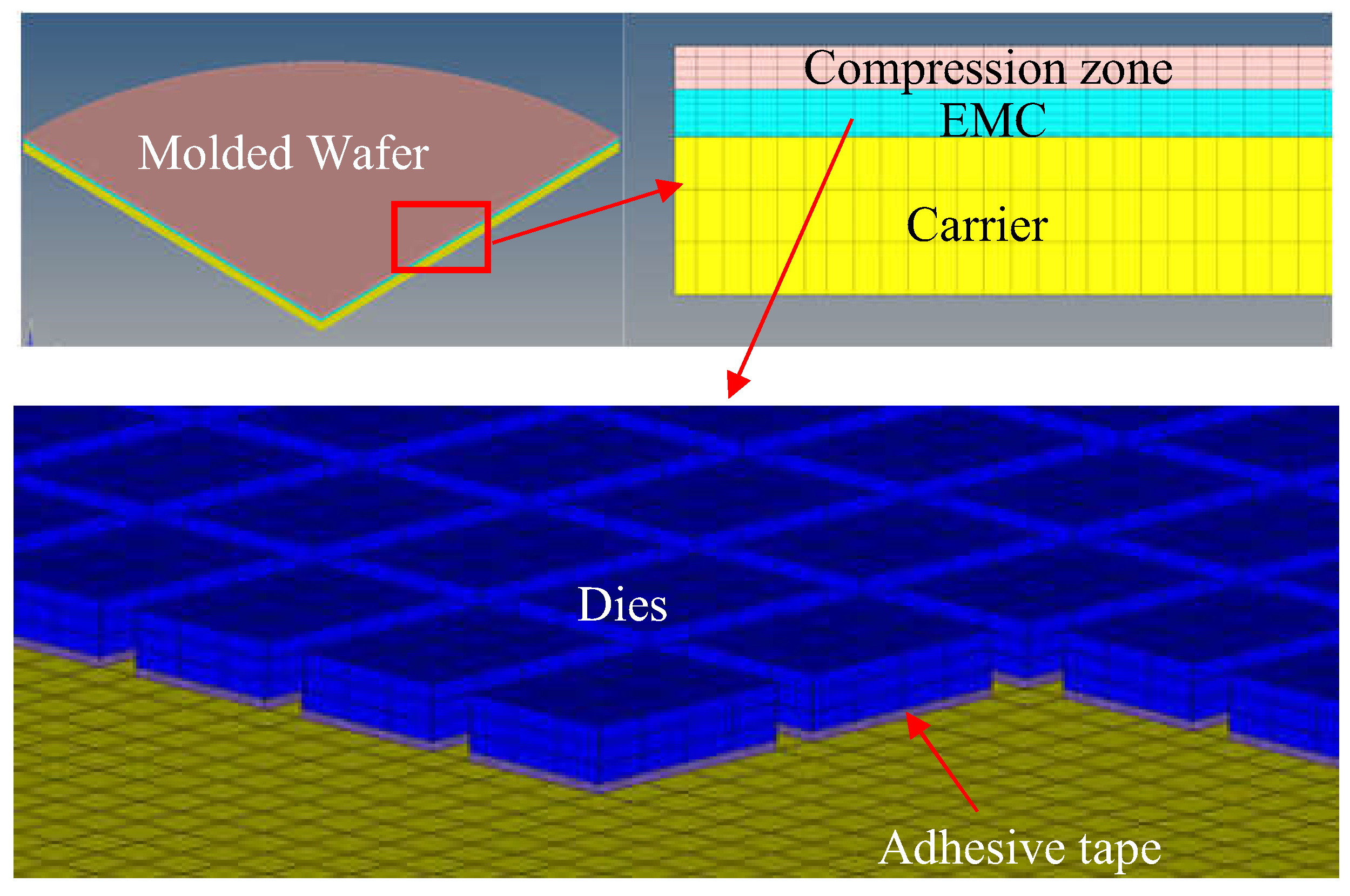
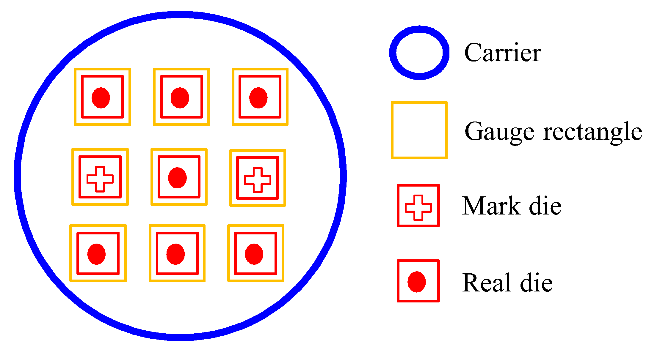
  • The known good dies diced from the wafer are mounted on the carrier by the die mounter with the active side facing down to realize the prespecified layout. The die height is 200 μ m , length and width is 737 μ m × 517 μ m , and the pitch is 150 μ m . There are about 50,000 dies on 8-inch wafers (radius 103.5 mm).
  • A plunger with a diameter of 198 mm. Once the mold is closed, the plunger begins to rise. The lower mold in Figure 2a is sprayed with a layer of spiral EMC in Figure 2b.
  • Different from [16], we adopt the spiral spray spiral parameters facilitating flow disperse. The basic parameters of the spiral is listed as: 23 turns, outer radius of 103.5 mm, spacing of 4.5 mm, and dispensing volume of 14.5 g as shown in Figure 2.
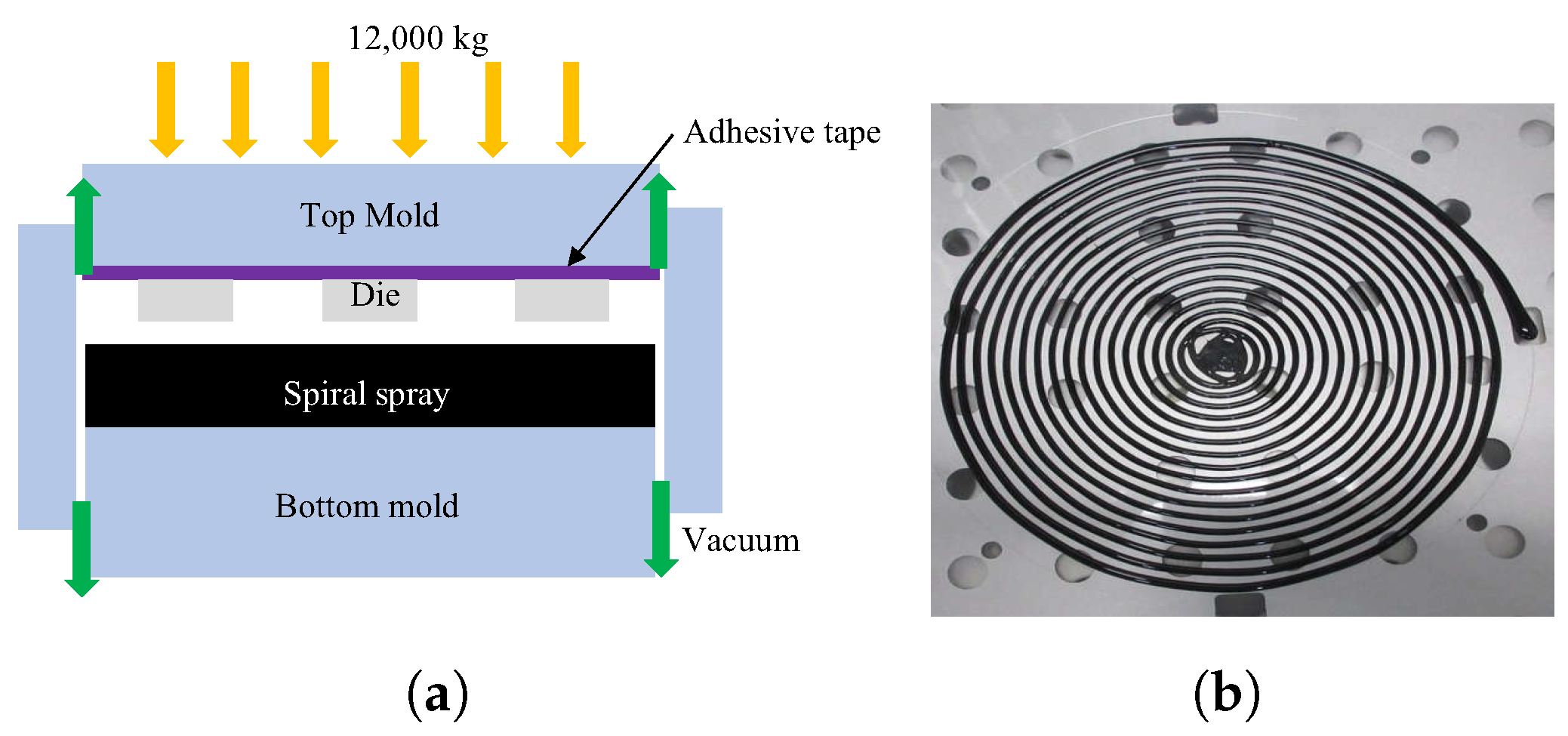
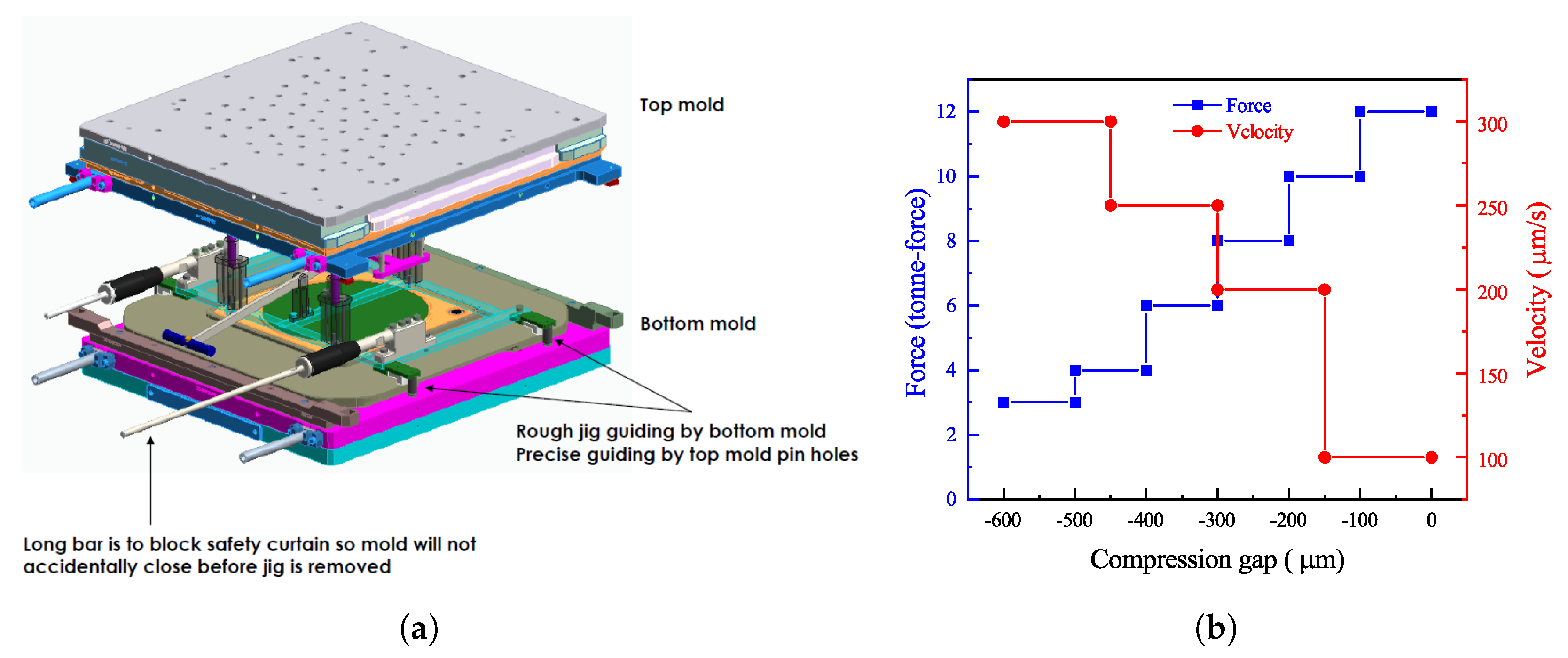
  • After 15 s, the EMC is compressed to fill the entire cavity (mold cap) and reaches the setting pressure (12 tons). The plunger stops moving, and the four fine-tuning motors increase or decrease according to the actual thickness of the mold cap. The buffering spring force of the plunger is generally 150∼450 Kg.
  • After 10 min of heat preservation, the EMC is cured, and the mold chamber is opened. Then, the wafer is removed by the hands of the operator or industrial robot, and the cooling stage is completed at the ambient temperature.

3. Mechanism of the Die Fly and Shift

3.1. Cohesive Zone Material Model for Debonding

As shown in Figure 4a, the testing apparatus (Instron ITW) is employed for characterizing the adhesive strength of the LiTaO3 die and adhesive tapes. Technically, from the peak value of the test signal, the shear strength is obtained with a temperature-controlled carrier between 80 C and 150 C. The peel strength concerned the total input energy for peel ( G c ) and the plastic bending energy ( G p ) during the peel, which are measured from the testing apparatus. Die fly and shift are activated by associating a cohesive zone material model with the contact elements. The peel strength is converted to the critical fracture energy to facilitate calculations. In terms of the vendor-supplied thermal release tape, the interfacial tension of the foaming adhesive surface in the expected condition (i.e., when the temperature is below 170 C) is around 2.015 N / cm . The value decreased to 0.035 N / cm after foaming. To characterize the traction–separation law shown in Figure 4b, from the test results and the commercial vendor’s data, the parameters of CZM employed in the contact interface element are listed in Table 1.
The interface behavior of CZM is described by a nonlinear traction–separation law (TSL), which has been modeled and measured extensively [17]. Since the brittle adhesive, the bilinear traction–separation law [18] is employed in this paper. By adopting the shear-lag model [19], the initiation and propagation of the debonding between the dies and the adhesive tape are predicted. Unlike the [14], the die shift and fly are altered under different modes, depending on the thermomechanical processes (heating or cooling). Here, the die fly is mimicked under the heating steps concerning the primarily mixed mode (shearing mode and normalizing mode), while the die shift is accumulated in the cooling stage.
Since the die fly can be equivalent to debonding behavior occurring in the tangential and normal direction, the mixed debonding mode is the appropriate choice. The CZM model consists of the constitutive relation between the strain u t acting on the horizontal interface and the vertical interface u n . The contact gap or penetration and tangential slip distance define the interface separation. The contact element type and the contact detection point’s location are used for contact and tangential slip calculations. The constitutive equations for the normal and tangential directions are written as follows:
σ = K n u n 1 d m τ = K t u t 1 d m d m = Δ n 2 + Δ t 2 1 Δ n 2 + Δ t 2 u n c u n c u n = Δ n 2 + Δ t 2 1 Δ n 2 + Δ t 2 u t c u t c u ¯ t
where σ denotes the normal contact stress, τ denotes the tangetial contact stress, K n is the normal contact stiffness, u n signifies the contact displacement, K t is the tangential contact stiffness, u t is the tangential contact displacement, u t c is the tangential slip distance after debonding completed, u ¯ n is the contact displacement at the maximum normal contact stress, u n c is the contact displacement at the completion of debonding, d m is the key factor for K m in mix mode slip, Δ n = u n u ¯ n , and Δ t = u t u ¯ t .
From Figure 4b, the traction–separation law similarly suits the sliding displacement along the tangential direction. Initially, the tangential displacement first increases with an initial stiffness K i . After a critical removal, the shear traction reaches its maximum, τ m a x . Then, the tangential stress decreases with further sliding due to energy accumulation at the interface. Eventually, the tangential stress is minimized to zero at another critical displacement, u t c , and the tangential stress remains zero as the interface is delaminated.

3.2. The Mathematical Model for Mold Flow

A mathematics pressure–volume–temperature (P-V-T) equation for epoxy molding compound [20] is employed to describe the intrinsic mechanism of volume change. The volume change, Δ V , was defined by the decrease in the height of a sample, Δ h , in the mold cavity. The chemical conversion varies with time in an isothermal state, as given by Equation (2). The volume shrinkage V s h at any instant can be expressed as a function of pressure P, temperature T, and the conversion factor C i .
The degree of curing (DOC) is elucidated by Equation (2), as shown in Figure 5a. The excellent fluidity before curing is the benefit of filling the gap between dies. Hence, the EMC is cured by sustaining 10 min under the 120 C. These curves can be fitted by Equation (2):
d α d t = k 1 + k 2 α m ( 1 α n )
where k 1 = A 1 exp E 1 R T , k 2 = A 2 exp E 2 R T , α is the curing degree, and A 1 , A 2 , E 1 , E 2 , k 1 , and k 2 are undetermined coefficients.
Through measurement, we found that under a constant temperature of 100∼200 C , there is no change in the viscosity after the EMC is maintained for 50 s. During the curing, the viscosity EMC is illuminated by Equation (2), as shown in Figure 5b. After 300 s, the viscosity is sharply upsurged until the maximum plateau value is met. These curves can be fitted by Equation (3):
η ( α , T ) = η 0 ( T ) α g α g α C 1 + c 2 α η 0 ( T ) = A exp E a / R T
where α g is the curing degree of epoxy resin when the curing process reaches the gel point and A, E a , C 1 , and C 2 are undetermined coefficients.
G ( t ) = G 0 1 i = 1 n g i + i = 1 n g i G 0 exp t / τ i G κ ( t ) = κ 0 1 i = 1 n k i + i = 1 n k i κ 0 exp t / τ i κ
It is described in the form of Prony series, which will be used in the subsequent stress analysis.
The modified two-domain Tait PVT model elucidates the function of the temperature and pressure for the density of the polymer. The EMC flow simulation during high temperatures depends on the PVT model’s dynamics. The two-domain Tait PVT model is demonstrated in the following equations, whose parameters are listed in Table 2.
V ( T , p ) = v 0 ( T ) 1 C ln 1 + p B ( T )
where V ( T , p ) is the specific volume at temperature and pressure, V 0 is the specific volume at zero gauge pressure and is determined below, T is the temperature, p is the pressure, C is a constant, 0.0894 , and B accounts for the pressure sensitivity of the material.

4. Simulation and Experiment for Die Fly

4.1. Mold Flow Simulation

By virtue of manufacturing line of Xiamen Sky Semiconductor Technology Co., Ltd., Xiamen, China, simulation and the manufacturing process are investigated with the aforementioned material property. In the high-temperature flow curing stage, after 10 s, the maximum fluid force occurred. The simulation boundary conditions are set as follows: the compression time is 10 s, the compression gap is 600 μ m, the maximum velocity is 300 μ m/s, and the maximum compression force is 12 ton. Referring to the molding devices settings, the wafer loading jig is illuminated in Figure 6a, which is conducted with the same default setting as in Figure 6b. Herein, the curve of compression gap and speed, the curve of compression force and void, and the compression interval are illustrated. In addition, the processing time is composed of the compression time, the cure time, and the geometry parameters, as illustrated in Table 3. The wafer level molding model is constructed in Figure 7, wherein the adhesive tape is set as CZM. In the simulation setting, the adhesive tape and die are treated as the mold core to conduct the casting process. Namely, we merely take the heat and compression procedure into account to obtain the stress induced from the molding flow and curing at high temperatures, ignoring the cooling stage. There is always some rest resin in order to form the perfect spiral. Initially, the rest resin is dotted in the center zone, as shown in Figure 8a. Then, it is dotted in the wafer periphery, as shown in Figure 8b.

4.1.1. Effect of Die Thickness

Due to the die fly induced by the multi-dimension direction effect, in three directions, the fourth strength theory for the failure explanation is employed. Figure 9 shows the simulated von Mises stress results with statistical distribution for different die thickness, i.e., 200 μ m , 175 μ m , and 100 μ m . It is observed that the die fly risk increases as the die thickness demonstrates backside thinning. This is due to increased fluid pressure acting on the die surfaces, while simultaneously, the relative volume ratio is increased by significantly increased curing shrinkage stress. In addition, as the dies become thinner, the epoxy molding compound fluid velocity on the top surface of the mold increases, and the impact force on the mold wall increases, resulting in an irregular flow of fluid in the die gap and causing die fly.

4.1.2. Effect of the Die Layout

In terms of the die layout in different radius ranges, as the die layout range increases, the impact force of the fluid on the die first increases and then decreases. The minimum stress of these layout is 0.592 MPa when it is close to whole laid, as shown in Figure 10. In addition, the blue zone always corresponds to the periphery without the spiral spray, while the red side is the periphery of the spiral spray.

4.1.3. Effect of the Spiral Layout

Generally, to reduce the die shift during the molding process, the compression filling speed is decreased, the thickness of the molded body is increased, the initial diameter of the molding compound is optimized, a low-viscosity molding compound material is selected, and a mold with a large surface area and a low die thickness is used. We employed a novel adhesion promoter and optimized the recipe of the molding process. We should find the equilibrium point between the viscosity and the filling completed degree, i.e., the gaps between the dies filled with a low viscosity fluid to avoid the die fly. Hence, the velocity of the filling of molding is of great engineering significance. Intuitively, the die fly will more likely occur in the periphery of the wafer, for the viscosity increased with the EMC flowing from the center to the edge. However, in the spiral spray sample, the result varies. Empirically, limited by the vacuum chamber’s volume, the spiral layout adjustment is crucial and adequate to the die fly. With the weight unchanged, the rest of EMC forming the perfect spiral line is sprayed to the wafer’s center or the peripheral. Thus, the von Mises stress distribution and the die fly layout are illuminated in Figure 11. Obviously, compared with the center compensation spiral in Figure 11a, the von Mises stress concerning peripheral compensation in Figure 12a is significantly decreased from 1.087 MPa to 0.677 Mpa. Since the helix is not left–right symmetrical and there is a filler gap on the left side of the helix, the stress value on the right side is smaller. In fact, given the vacuum effect, i.e., the airflow is ignored in mold flow simulation, the simulation results reflect the possibility of die fly. Under the default setting recommended by vendors, numerous die flies (Figure 11b), located in the von Mises notable region in Figure 11a, verified the simulation results. Moreover, the vacuum hole is located below these places, which can cause the die fly to occur.

4.2. Optimization Scheme

From Table 4, by fine-tuning the dies’ thickness and the spray’s layout and adding a layer of adhesion promoter, the whole wafer without the die fly flaw is obtained, as shown in Figure 12a. The value of the von Mises stress is significantly decreased when the filling speed is reduced to 30 μ m/s. Therefore, the multiple-step compression top mold with high-velocity values is inferior to the speed with a constant low-velocity value of 30 μ m/s. Namely, given that the compression gap is short, the total executed time is only increased to 20 s, and the known good die yields are significantly upsurged.

5. Simulation and Experiment for Die Shift

Initially, the glass carrier with a metalized gauge rectangle is designed and made with the physical vapor deposition (PVD) and wet etch process, as shown in Figure 13. After the mounter device completes die attaching, the back of the die is measured from center to periphery. Based on these measurements, compensation data to the mounter can be collected by benchmarking with the left mark. An automatic image device CHOTEST measures the die and gauges the rectangle’s relative gap in the horizontal and vertical directions. The automatic image device CHOTEST establishes coordinate data through a sample measurement, drawing calculation, and import data. Since the opaque EMC, die shift cannot be measured directly after the wafer molding, but can only be measured from the transparent glass carrier.

5.1. Optimization of the Die Shift Using Mounter Compensation

In terms of the die mounter, from the three horizontal and vertical paths, we obtain the distribution of the die shift with the electron microscope by benchmarking the gauge of the glass. The die shift rule induced by the mounter is: for the horizontal direction, the average is 1.5 μ m and maximum is 4 μ m, while in the vertical direction, the standard is 3 μ m and maximum is 7 μ m, as shown in Figure 14.
By controlling the die attach compensation of the machine, the mechanical error of the attachment itself, the impact of the fluid on the chip, the mismatch of the cooling shrinkage, and the chip offset caused by the external force of the vacuum machine can be compensated. Compensation is divided into three areas according to the die shift’s scale after the die attach. After repeated iterative calibration of the simulation with actual experience, we optimized the patch recipe from the predicted chip offset value, maximizing the chip offset’s compensation. The measured die shift after molding shows that the method is efficient and feasible. By setting the cure temperature as the reference point, the die shift results in comparison are demonstrated in Figure 15a,b. Given that the adjacent dies have a relative die shift concerning the glass gauge, we further ensure die attachment compensation. Consequently, in Figure 15c,d, the die shift can be controlled within 70 μ m for both directions. Given that the opening diameter of the first passivisation layer is not large than 100 μ m, when the die shift is greater than 40 μ m, the merits of the FOWLP cannot be realized with mass production. The high yield should be taken into account to adapt the needs of manufacture.

5.2. Alternative of EMC with Thermosetting Films

The excellent flow mobility of EMC may not, as is often assumed, be its most compelling feature from device packaging. Although the spiral dispensing can better adapt the fluid impact of molten EMC on the die, considering the process capability of the equipment, we recommend reducing the number of die layouts on the periphery of the wafer and adjusting the spiral dispensing. The layout of the die and adding adhesion promoters can solve the die fly. After placement on a vacuum laminator, a thickness of 100 μ m thermosetting epoxy resin film is employed. It only needs to control the CTE of the carrier and the curing temperature curve to obtain a slight die shift. In terms of thickness, a plastic-encapsulated wafer with a specified thickness can be completed based on multiple vacuum lamination processes. This method has better process compatibility for high CTE and ultrafine dies. The process of the vacuum suction film technique is demonstrated in Figure 16. By choosing a suitable CTE and Young’s modulus thermosetting films, the die shift is decreased in Figure 17b, while Figure 17a is the die shift for A-film cured. In Figure 17a, the results are deteriorated. With A-film compression and cure, dies are even shifted out of the rectangle. However, corresponding to Figure 17b, the die shift for the two directions is measured, as shown in Figure 18, which illuminates the die shift limited to 50 μ m. Empirically, the count of the die shift in the interval of 40 to 50 μ m is too small (less than 5%) to affect the high yield. Thereby, it is comparable to the silicon die wafer molding results [7] to facilitate the next step of the FOWLP.

6. Conclusions

This paper informatively alleviates the die fly challenge in the conventional EMC molding process and obtains the die fly rule for the SAW filters with FOWLP. We have successfully controlled the die shift within 50 μ m, while none of the die flies occurred in the wafer with nearly 5000 dies. The process parameters optimization is performed from the design and optimization of the channel structure of the molding flow and the fluid-curing coupling simulation. Verified by the experiment, the problem of the submillimeter die fly is solved. The predicted die shifts during molding cooling agree with the online measurement data, demonstrating the validity of the proposed theoretical model. Some other critical concluding observations are listed as follows:
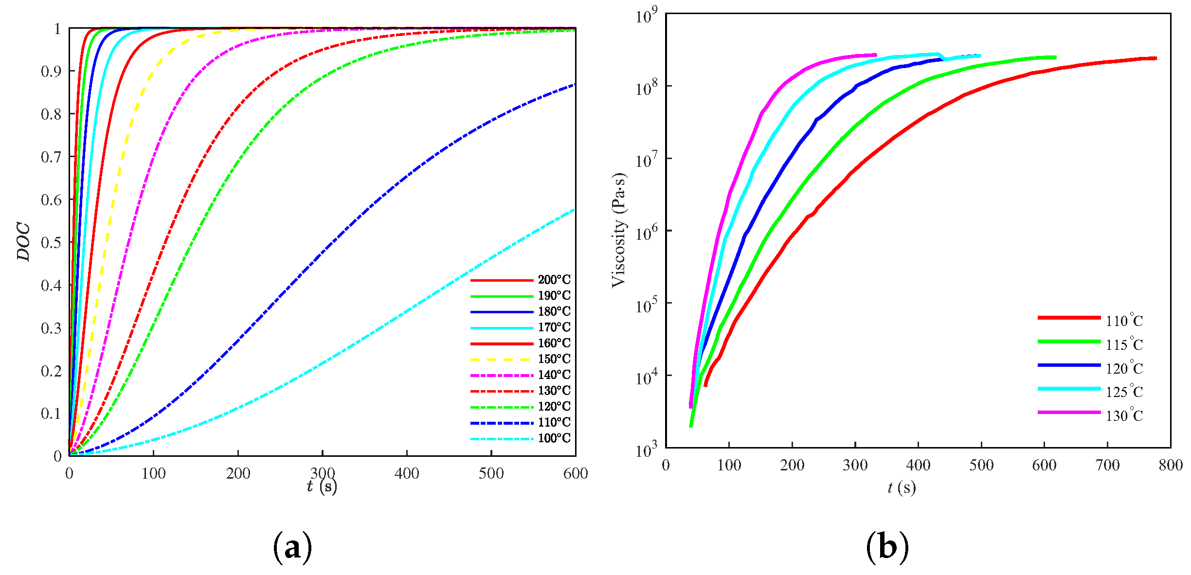
  • The impact of fluid on the chip and bonding layer was analyzed with an experiment. The adhesive layer was equivalent to the CZM layer, and the curve law of the fluid viscosity and DOC of EMC were used for mode flow simulation. The von Mises stress was employed to evaluate the comprehensive stress on the adhesive layer.
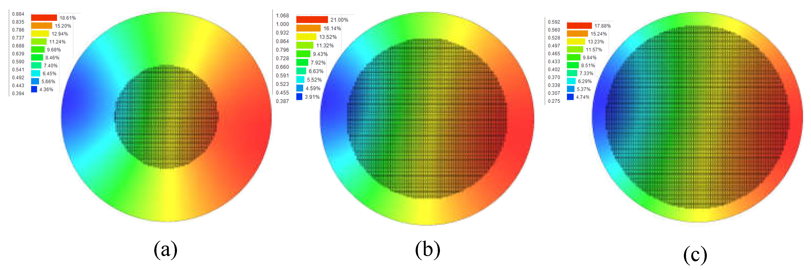
  • With the optimization of a process parameter, 100 kPa vacuum pressure, a speed of the top mold of 30 μ m/s, and a modified layout of the spiral and geometry of the die, the die fly is shut out to realize the high yield.
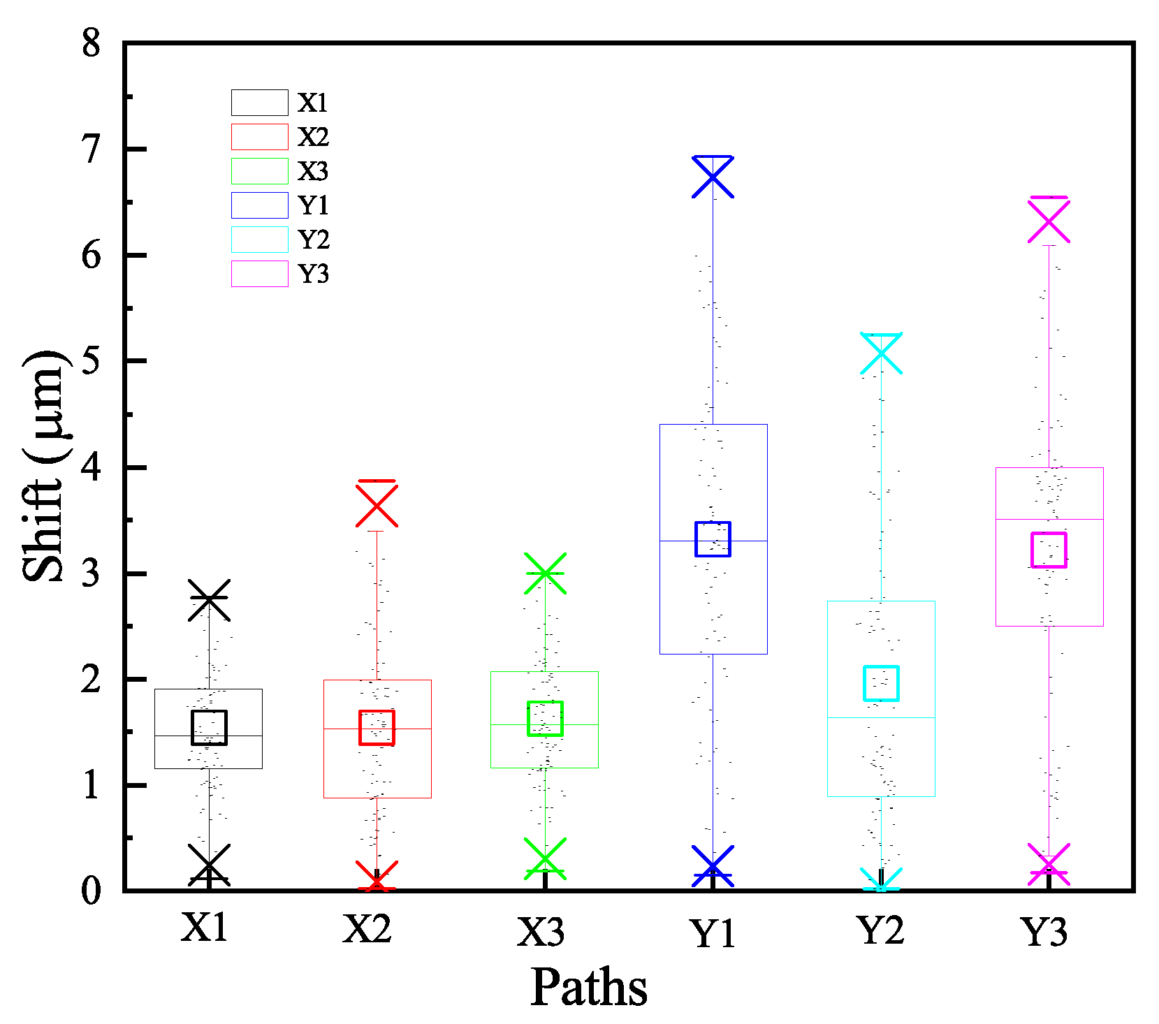
  • In the cooling stage, the die shift suffers from the viscoelastic dynamic of the EMC and the anisotropy of LiTaO3. Since the die shift is linearly increased along the radius direction, the die shift issue is mitigated through the compensation in the premium stage of the die mounter.
  • Based on the vacuumed filling principle, a novel thermosetting film can avert the die fly and control the die shift by optimizing the film thickness and the compression process.

Author Contributions

Conceptualization, W.L.; methodology, W.L.; software, W.L.; experimental validation, W.L.; supervision, D.Y.; project administration, D.Y.; funding acquisition, D.Y. All authors have read and agreed to the published version of the manuscript.

Funding

This work was supported by the Science and Technology Major Project of Xiamen City, China (3502Z20201004).

Data Availability Statement

Due to researcher’s confidential interest, the data are unavailable.

Acknowledgments

The author would like to thank Jibao Lu, Yulong Li from the Shenzhen Institute of Advanced Technology, Chinese Academy of Sciences, Jianhong Huang, Jingbo Xiao, Houdun Zhang, and Binbin Zhou at Xiamen Sky Semiconductor Technology Co., Ltd. for their experimental support.

Conflicts of Interest

The authors declare no conflict of interest.

References

  1. Zhang, X.; Wang, Q.; Wang, B.; Wang, G.; Gu, X.; Chen, Y.; Tan, L.; Zhou, S.; Cai, J. A hybrid antenna in package solution using fowlp technology. J. Electron. Packag. 2022, 144, 031005. [Google Scholar] [CrossRef]
  2. Braun, T.; Becker, K.F.; Hoelck, O.; Voges, S.; Kahle, R.; Graap, P.; Wöhrmann, M.; Aschenbrenner, R.; Dreissigacker, M.; Schneider-Ramelow, M.; et al. Fan-out wafer level packaging-a platform for advanced sensor packaging. In Proceedings of the 2019 IEEE 69th Electronic Components and Technology Conference (ECTC), Las Vegas, NV, USA, 28–31 May 2019; pp. 861–867. [Google Scholar]
  3. Li, W.; Yu, D. Experimental and numerical investigations of the warpage of fan-out wafer-level packaging with saw filters. IEEE Trans. Components Packag. Manuf. Technol. 2022, 12, 869–877. [Google Scholar] [CrossRef]
  4. Yu, D.; Jiang, F.; Zhang, X. A Kind of Fan-Out Packaging Structure and Packaging Method for Filters. CHN Patent CN202010962125.8, 12 February 2021. (In Chinese). [Google Scholar]
  5. Lau, J.H.; Li, M.; Tian, D.; Fan, N.; Kuah, E.; Kai, W.; Li, M.; Hao, J.; Cheung, Y.M.; Li, Z.; et al. Warpage and thermal characterization of fan-out wafer-level packaging. IEEE Trans. Components Packag. Manuf. Technol. 2017, 7, 1729–1738. [Google Scholar] [CrossRef]
  6. Sharma, G.; Rao, V.S.; Kumar, A.; Su, N.; Ying, L.Y.; Houe, K.C.; Lim, S.; Sekhar, V.N.; Rajoo, R.; Kripesh, V.; et al. Embedded wafer level packages with laterally placed and vertically stacked thin dies. In Proceedings of the 2009 59th Electronic Components and Technology Conference, San Diego, CA, USA, 26–29 May 2009; pp. 1537–1543. [Google Scholar]
  7. Sharma, G.; Kumar, A.; Rao, V.S.; Ho, S.W.; Kripesh, V. Solutions strategies for die shift problem in wafer level compression molding. IEEE Trans. Components Packag. Manuf. Technol. 2011, 1, 502–509. [Google Scholar] [CrossRef]
  8. Ji, L.; Kim, H.J.; Che, F.; Gao, S.; Pinjala, D. Numerical study of preventing flow-induced die-shift in the compression molding for embedded wafer level packaging. In Proceedings of the 2011 IEEE 13th Electronics Packaging Technology Conference, Singapore, 7–9 December 2011; pp. 406–411. [Google Scholar]
  9. Bu, L.; Ho, S.; Velez, S.D.; Chai, T.; Zhang, X. Investigation on die shift issues in the 12-in wafer-level compression molding process. IEEE Trans. Components Packag. Manuf. Technol. 2013, 3, 1647–1653. [Google Scholar]
  10. Ji, L.; Sorono, D.V.; Chai, T.C.; Zhang, X. 3-d numerical and experimental investigations on compression molding in multichip embedded wafer level packaging. IEEE Trans. Components Packag. Manuf. Technol. 2012, 3, 678–687. [Google Scholar] [CrossRef]
  11. Sun, Y.; Hou, F.; Chen, F.; Liu, H.; Zhang, H.; Sun, P.; Lin, T.; Cao, L. Compensation method for die shift in fan-out packaging. In Proceedings of the 2018 19th International Conference on Electronic Packaging Technology (ICEPT), Shanghai, China, 8–11 August 2018; pp. 1681–1686. [Google Scholar]
  12. Fowler, M.; Massey, J.P.; Braun, T.; Voges, S.; Gernhardt, R.; Wohrmann, M. Investigation and methods using various release and thermoplastic bonding materials to reduce die shift and wafer warpage for ewlb chip-first processes. In Proceedings of the 2019 IEEE 69th Electronic Components and Technology Conference (ECTC), Las Vegas, NV, USA, 28–31 May 2019; pp. 363–369. [Google Scholar]
  13. Mazuir, J.; Olmeta, V.; Yin, M.; Pares, G.; Planchais, A.; Inal, K.; Saadaoui, M. Evaluation and optimization of die-shift in embedded wafer-level packaging by enhancing the adhesion strength of silicon chips to carrier wafer. In Proceedings of the 2011 IEEE 13th Electronics Packaging Technology Conference, Singapore, 7–9 December 2011; pp. 747–751. [Google Scholar]
  14. Hsiao, C.-L.; Yang, C.-Y.; Chen, H.-C.; Yang, T.-S.; Chen, K.-S.; Wu, T.-H.; Wang, Y.-C.; Lee, S. Identification of curing kinetics of epoxy molding compounds and mold flow analysis for assessment of die-shift defects. In Proceedings of the 2017 12th International Microsystems, Packaging, Assembly and Circuits Technology Conference (IMPACT), Taipei, Taiwan, 25–27 October 2017; pp. 42–45. [Google Scholar]
  15. Li, W.; Xue, K.; Chen, H.; Lee, K.; Cheng, G.; Wu, J. Failure mechanism of fly die in eutectic bonding. IEEE Trans. Components Packag. Manuf. Technol. 2015, 5, 838–844. [Google Scholar] [CrossRef]
  16. Cheng, H.-C.; Chung, C.-H.; Chen, W.-H. Die shift assessment of reconstituted wafer for fan-out wafer-level packaging. IEEE Trans. Device Mater. Reliab. 2020, 20, 136–145. [Google Scholar] [CrossRef]
  17. Jaillon, A.; Jumel, J.; Paroissien, E.; Lachaud, F. Mode i cohesive zone model parameters identification and comparison of measurement techniques for robustness to the law shape evaluation. J. Adhes. 2020, 96, 272–299. [Google Scholar] [CrossRef]
  18. Sharma, V.P.; Datla, N.V. Effect of bond-line thickness and mode-mixity on the fracture behavior and traction separation law of sn-0.7 cu solder joints. Eng. Fail. Anal. 2022, 131, 105855. [Google Scholar] [CrossRef]
  19. Moradi, M.; Sivoththaman, S. Strain transfer analysis of surface-bonded mems strain sensors. IEEE Sens. J. 2012, 13, 637–643. [Google Scholar] [CrossRef]
  20. Deng, S.-S.; Hwang, S.-J.; Lee, H.-H. Warpage prediction and experiments of fan-out waferlevel package during encapsulation process. IEEE Trans. Components Packag. Manuf. Technol. 2013, 3, 452–458. [Google Scholar] [CrossRef]
Figure 1. (a) The packaging process flow of the FOWLP. (b) The scheme for die fly and die shift.
Electronics 12 02073 g001
Figure 2. (a) The sketch of molding. (b) Spiral spray epoxy molding compound.
Electronics 12 02073 g002
Figure 3. The sketch of the adhesive tape construction.
Electronics 12 02073 g003
Figure 4. (a) The shear strength measurement device. (b) The principle of the debonding failure.
Electronics 12 02073 g004
Figure 5. (a) The temperature-dependent DOC changes in the first 10 min. (b) The viscosity of the EMC.
Electronics 12 02073 g005
Figure 6. (a) Wafer loading jig. (b) The multi−stage velocity and force default setting.
Electronics 12 02073 g006
Figure 7. The meshed CFD model using Moldex3D.
Electronics 12 02073 g007
Figure 8. (a) The initial layout of the spiral. (b) The modified layout of the spiral.
Electronics 12 02073 g008
Figure 9. The effect of die thickness.
Electronics 12 02073 g009
Figure 10. The effect of the die layout. (a) Die attached in 4 inch range. (b) Die attached in 6 inch range. (c) Die attached in 8 inch range.
Electronics 12 02073 g010
Figure 11. (a) The von Mises stress distribution of the center compensation spiral. (b) The die fly layout by the default process.
Electronics 12 02073 g011
Figure 12. (a) The von Mises stress distribution of the peripheral compensation of the spiral. (b) The perfect wafer by the optimization scheme.
Electronics 12 02073 g012
Figure 13. The sketch of the die shift measurement.
Electronics 12 02073 g013
Figure 14. The die shift after the mounter for the six paths.
Electronics 12 02073 g014
Figure 15. (a) The die shift distribution in the horizontal direction before optimization. (b) The die shift distribution in the vertical direction before optimization. (c) The die shift distribution in the horizontal direction after optimization. (d) The die shift distribution in the vertical direction after optimization.
Electronics 12 02073 g015
Figure 16. (a) Opening and cleaning of the chamber. (b) Layout the wafer attached with dies and covered with the film. (c) Closing of the chamber and conducting the compression with vacuum. (d) Opening and cooling of the chamber.
Electronics 12 02073 g016
Figure 17. (a) The die shift located in the marked zone after being cured with A-film. (b) The die shift located in the marked zone after being cured with B-film.
Electronics 12 02073 g017
Figure 18. The count of the optimized die shift for the thermosetting film compression.
Electronics 12 02073 g018
Table 1. Parameters of the cohesive zone model.
ParametersSymbolValues
Maximum normal stress σ max 0.87 MPa
Critical fracture energy
density for normal separation
G cn 201.5 J / m 2
Maximum tangential stress τ max 0.87 MPa
Critical fracture energy density for tangential slip G ct 201.5 J / m 2
Artificial damping coefficient η 1.00 × 10 3 s
Flag for tangential slip under
compression stress
β 1
Table 2. Parameters of the modified two-domain Tait PVT model.
ParametersCuredRawUnit
b 1 L 0.59340.5859cc/g
b 2 L 0.0001530.000153cc/(g·K)
b 3 L 4.37 × 10 9 7.144 × 10 9 dyne / cm 2
b 4 L 0.0094290.012541/K
b 1 S 0.5930.5859cc/g
b 2 S 6.705 × 10 5 6.705 × 10 5 cc/(g·K)
b 3 S 5.308 × 10 9 7.34 × 10 9 dyne / cm 2
b 4 S 0.0050060.010071/K
b 5 418.1323.1K
b 6 4.495 × 10 9 3.337 × 10 9 cm 2 ·K/dyne
Table 3. Geometry parameters of the FOWLP.
ComponentsDimensions
Die 740 × 520 × 200   μ m (8-inch wafer)
Adhesive30 μ m (thickness)
Glass1100 μ m (thickness)
Die pitch150 μ m (width)
EMC300 μ m (thickness)
Table 4. Optimized process for the wafer molding.
ItemsData
Die thickness200 μ m
Over mold thickness100 μ m
Compression velocityConstant with 30 μ m/s
Die layoutFull laid
SpiralPeripheral compensation
Vacuum pressure100 kPa
Disclaimer/Publisher’s Note: The statements, opinions and data contained in all publications are solely those of the individual author(s) and contributor(s) and not of MDPI and/or the editor(s). MDPI and/or the editor(s) disclaim responsibility for any injury to people or property resulting from any ideas, methods, instructions or products referred to in the content.

