Communication

On the Minimum Value of Split DC Link Capacitances in Three-Phase Three-Level Grid-Connected Converters Operating with Unity Power Factor with Limited Zero-Sequence Injection

1
School of Electrical and Computer Engineering, Ben-Gurion University of the Negev, Beer-Sheva 8410501, Israel
2
Department of Electrical Engineering and Electronics, Ariel University of Samaria, Ariel 40700, Israel
3
Department of Mechanical Engineering and Mechatronics, Ariel University of Samaria, Ariel 40700, Israel
4
Department of Electrical and Electronics Engineering, Shamoon College of Engineering, Beer-Sheva 8410802, Israel
*
Author to whom correspondence should be addressed.
Electronics 2023, 12(9), 1994; https://doi.org/10.3390/electronics12091994
Submission received: 14 March 2023 / Revised: 23 April 2023 / Accepted: 24 April 2023 / Published: 25 April 2023
(This article belongs to the Special Issue Single-Stage DC-AC Power Conversion Systems)

Abstract

:
This paper introduces an approach to calculating the minimum value of split DC link capacitance in three-phase three-level grid-connected DC-AC converters operating with unity power factor without either active balancing circuits or AC zero sequence injection. Due to the fact that partial DC link voltages and rectified mains phase voltages reach their maximum and minimum values, respectively, at different time instants, it is feasible to decrease the minimum value of the former below the maximum value of the latter while still maintaining proper functionality of the power stage. The minimum possible split DC link capacitance values are hence derived from the boundary condition where the above-mentioned voltages are tangent to each other. The accuracy of the analytical derivations is confirmed by simulations and experiments carried out on a 10 kVA T-type converter prototype, which show a high degree of agreement.

1. Introduction

Grid operators have established rigorous guidelines for maintaining high standards of mains current quality, which is measured in terms of total harmonic distortion (THD) [1,2]. As a result, power converters that are connected to the grid are required to ensure that the mains current waveform is almost sinusoidal and synchronized with the grid voltage, i.e., to operate with unity power factor [3]. Grid-connected power converters usually incorporate short-term energy storage components (typically in the form of capacitors) on the DC side in order to deal with pulsating power components [4], maintain desired operation during power mismatches that occur during transients [5] and provide hold-up energy (if necessary) [6].
Regrettably, DC link capacitance is often the limiting factor for reliability and/or physical size in grid-connected power conversion systems [7,8,9]. The value of required DC link capacitance is usually determined by hold-up time requirements. Conversely, for certain applications where short loss of mains may be handled, hold-up energy storage is unnecessary. In such cases, it may be feasible to decrease the amount of DC link capacitance. Various common methods for reducing the required amount of DC link capacitance have been proposed so far, including:
-
Active power decoupling [10,11,12];
-
Distorting the mains current to the lowest permissible power quality level [13,14];
-
Increasing the DC link voltage ripple [15,16].
-
The literature provides minimum values of DC link capacitance for:
-
Single-phase grid-connected converters that employ active power decoupling circuitry [17];
-
Line waveform control [14];
-
PI + Notch DC link voltage controllers [18];
-
Increased DC link ripple [16].
In three-phase converters operating under balanced conditions, the pulsating power component is eliminated at the DC side [19], resulting in a relatively small total DC link capacitance requirement for two-level three-phase converters [20]. Nevertheless, Ref. [21] conducted minimum DC link capacitance sizing based on stability requirements for photovoltaic inverters. Recently, three-level three-phase AC/DC and DC/AC converters with split two-capacitors DC links have emerged as a viable topology for power ratings ranging from 10 kVA to 100 kVA [22] (it should be emphasized that inverters producing more than three-levels of voltage containing multiple-split-capacitors DC links [23,24] are not addressed in this work). However, systems that use split DC links introduce an interesting phenomenon as follows: despite the absence of a pulsating power component at the DC side, split DC link capacitors in such systems are still subject to oscillating power components even though they sum up to zero. When the midpoint of the split DC link capacitors is isolated from the mains neutral line, it is feasible to remove the resultant ripples in the partial DC link voltage. This can be accomplished by supplementing the modulating signal with a third-harmonic zero-sequence component (in the case of a converter operating at unity power factor) in addition to the DC component, which is necessary for balancing the average values of split DC link voltages [25,26,27,28]. However, to prevent grid-side currents from containing zero-sequence components, it is important to avoid injecting high-frequency zero sequence components in three-phase four-wire three-level converters. Furthermore, the presence of high-frequency zero components can result in common mode currents in transformerless grid-connected photovoltaic systems [29]. If minimizing DC link capacitance is desired in such systems, it can be achieved by using additional specialized hardware, as suggested in [30,31]. Nevertheless, it should be noted that this solution would come at the expense of increased system cost and physical size. Recently, a methodology has been proposed in [30] to establish a baseline for split DC link capacitance values and voltage set points in three-phase three-level AC/DC (or DC/AC) converters. This methodology applies to converters that operate with unity power factor and a zero-sequence component injected into modulation signals comprising solely a DC component. The present study merges the approach introduced in reference [32] with the concept proposed in [15] to ascertain the lowest achievable values of split DC link capacitance through maximal increase of DC link voltage ripple. It is shown that the proposed methodology allows the attainment of a two-fold reduction of utilized DC link capacitance compared to the technique proposed in [32]. The proposed approach is validated through simulations and experiments.

2. Materials and Methods

A generalized three-phase three-level grid-connected AC-DC power converter operating with unity power factor which the present study focuses on is depicted in Figure 1 [33]. Possible realizations of three-way switches SR, SS and ST may be found in [34,35,36]). The AC side of the converter is interfaced to the grid via L or LCL filters while its DC side is linked with either a two- or three-terminal equivalent power element, representing a downstream converter [37]. The split DC link is realized by two capacitors, namely CDC1 and CDC2.
Referring to Figure 1, vectors of mains voltages and currents are given by
v R S T t = v R N t v S N t v T N t = V M s i n ω t s i n ω t φ s i n ω t + φ i R S T t = i R t i S t i T t = I M s i n ω t s i n ω t φ s i n ω t + φ
with φ = 2 π / 3 . Consequently, the corresponding pulse-width modulation signals vector is approximately (neglecting voltage drops across filter components) given by
m R S T t = m R t m S t m T t M t s i n ω t s i n ω t φ s i n ω t + φ + m 0 t
with M(t) and m0(t) denoting the modulation index and zero-sequence component (restricted to DC in this work), respectively. Corresponding converter-imposed AC-side voltages are given by
v A B C t = v A O t v B O t v C O t = m A B C t · v D C 1 t , m A B C t > 0 v D C 2 t , m A B C t < 0
with vDC1(t) and vDC2(t) denoting partial DC link capacitors CDC1 and CDC2 voltages, respectively. Considering (1), the instantaneous AC-side phase power vector is given by
p R S T t = p R t p S t p T t = v R N t i R t v S N t i S t v T N t i T t = V M I M 2 1 c o s   2 ω t 1 c o s   2 ω t φ 1 c o s   2 ω t + φ ,
hence total AC-side power is ripple-free,
p R S T t = p R t + p S t + p T t = 3 2 V M I M = P R S T .
On the other hand, assuming that DC-side steady-state instantaneous power is also constant, given by
p L t = P L ,
the instantaneous system power balance (neglecting conversion losses and energy stored in filter components) is given by
P R S T = P L .
Consequently, pC(t) = pC1(t) + pC2(t) = 0 in steady state and the total DC link voltage vDC(t) is low-frequency-ripple-free. While AC-side voltages v R S T t and currents i R S T t do not contain any zero-sequence components, converter AC-side voltages v A B C t may contain such components in case of nonzero m0(t). Consequently, converter-imposed DC-side partial power vectors are obtained as
p A 1 B 1 C 1 t = p A 1 t p B 1 t p C 1 t = v A O t i R t = p R t + p 0 t 3 v B O t i S t = p S t + p 0 t 3 v C O t i T t = p T t + p 0 t 3 , i A B C t > 0 0 , i A B C t < 0 p A 2 B 2 C 2 t = p A 2 t p B 2 t p C 2 t = 0 , i A B C t > 0 v A O t i R t = p R t p 0 t 3 v B O t i S t = p S t p 0 t 3 v C O t i T t = p T t p 0 t 3 , i A B C t < 0
with p0(t) denoting the zero-sequence power component originated by m0(t). Consequently, converter-imposed DC-side partial powers are given by (cf. (7)) [32]
p A B C 1 t = p A 1 t + p B 1 t + p C 1 t P L 2 + p 0 t + P L 6 s i n 3 ω t p A B C 2 t = p A 2 t + p B 2 t + p C 2 t P L 2 p 0 t P L 6 s i n 3 ω t .
In case average components of split DC link capacitors’ voltages are balanced, then m0(t) (and thus p0(t)) are constant. Consequently, steady-state partial DC link capacitors’ powers are given by
p C 1 t = v D C 1 t C D C 1 d v D C 1 t d t P L 6 s i n 3 ω t p C 2 t = v D C 2 t C D C 2 d v D C 2 t d t P L 6 s i n 3 ω t .
In case set points of split DC link capacitor voltages are given by V D C 1 and V D C 2 , respectively, corresponding steady-state DC link capacitors’ voltages are obtained as [32]
v D C 1 t = V D C 1 1 P L 9 ω V D C 1 2 C D C 1 c o s 3 ω t , v D C 2 t = V D C 2 1 + P L 9 ω V D C 2 2 C D C 2 c o s 3 ω t .
Furthermore,
V D C 1 = V D C 2 = V D C , C D C 1 = C D C 2 = C D C
are typically employed, hence (11) may be generalized into
v D C 1 , 2 t = V D C 1 ± P L 9 ω V D C 2 C D C c o s 3 ω t .
Denoting the voltage rating of the split DC link capacitors as VR, maximum steady-state capacitors’ voltages should be set to αVR with α < 1 to allow a safety margin for prolonging the lifetime of the devices, imposing (cf. (13))
V D C 1 + P L 9 ω V D C 2 C D C = α V R .
Hence, split DC link capacitance value must satisfy
C D C = P L 9 ω V D C 2 α V R V D C 2 1 .
On the other hand,
v D C 1 , 2 t v R S T t
must hold at all times to allow correct functionality of the converter in Figure 1, imposing the boundary condition (cf. (1) and (13))
V M sin ω t = V D C 1 P L 9 ω V D C 2 C D C cos 3 ω t ,  
yielding tangency of partial DC link voltage and grid phase voltage. Hence, split DC link capacitance value must also satisfy
C D C = P L 9 ω V D C 2 1 V M sin ω t V D C 2 cos 3 ω t .
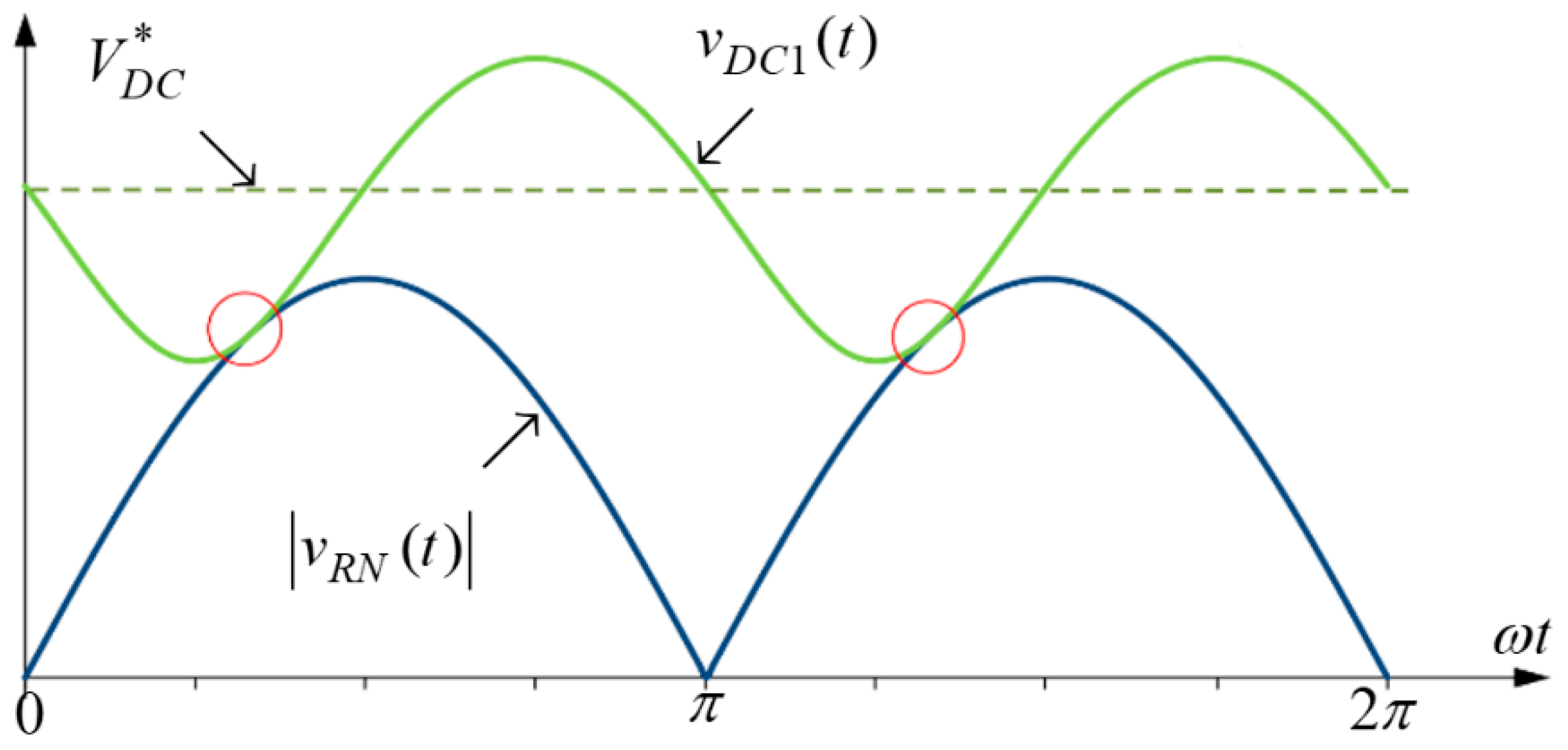
It is important to emphasize that the boundary condition allows the minimum value of partial DC link voltage to be lower than the maximum value of the rectified grid phase voltage, as illustrated in Figure 2. Such a situation was not considered in [32]. Consequently, the two boundary conditions yield the system of the two Equations (15) and (18) which must be solved simultaneously to obtain the required values of V D C and CDC. In order to eliminate the trigonometric form of (18), note first that
cos 3 ω t = 4 c o s 3 ω t 3 c o s ω t ,   s i n 2 ω t = 1 c o s 2 ω t .
Then, defining
x = cos ω t ,
letting
a = V M 2 V D C 2   ,   b = P L 9 ω V D C 2 C D C  
and substituting (19)–(21) into (18) yields
x 3 a 4 b x 2 3 4 x + a 1 4 b = 0 .
Solving (22) and applying (21) returns
C D C = 2 P L 9 ω V D C 2 3 72 1331 V M 8 V D C 8 9680 V M 6 V D C 6 + 22176 V M 4 V D C 4 20736 V M 2 V D C 2 + 6912 3 V M 8 V D C 8 + 23 24 · V M 4 V D C 4 + 2 .  
Combining (15) with (23) yields
1 α V R V D C 2 1 = 2 3 72 1331 V M 8 V D C 8 9680 V M 6 V D C 6 + 22176 V M 4 V D C 4 20736 V M 2 V D C 2 + 6912 3 V M 8 V D C 8 + 23 24 · V M 4 V D C 4 + 2 ,  
which may be solved using any available computational package to obtain the value of V D C . Then, CDC should be obtained by substituting the resulting value of V D C with (15).

3. Verification

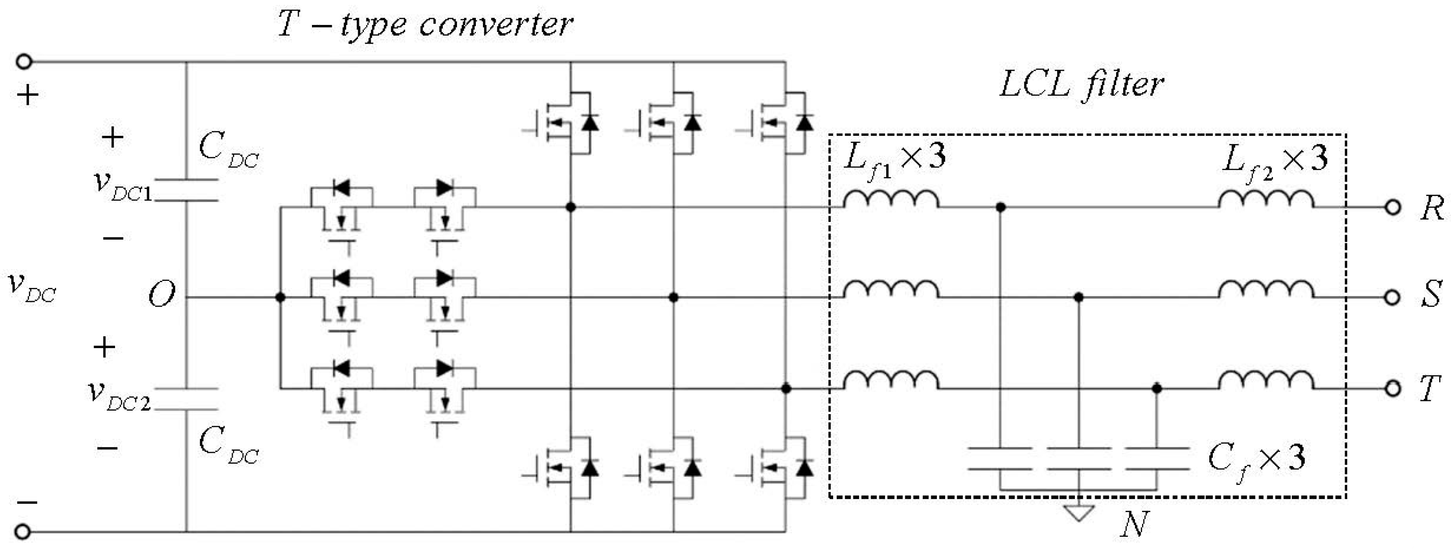
In order to verify the proposed methodology, consider a 10 kVA LCL-filter-based three-phase three-level T-type converter, shown in Figure 3. The corresponding system parameters are summarized in Table 1.
Simultaneous solution of (15) and (23) for the parameters in Table 1 results in
V D C = 327.25 V , C D C = 430 μ F .
The graphical solution is shown in Figure 4 for demonstration purposes, where the “maximum voltage imposed value” curve relates to (15) while the “minimum voltage imposed value” curve relates to (23). It is well-evident that upper and lower bound constraints on DC link voltage yield a single optimal solution.
In order to compare the required DC link capacitances’ values obtained using the methodology proposed in this paper to the results presented in [32], the value of V D C in (24) was substituted with [32], Equation (19), while taking into account the constraint stated in Section 3B of [32], namely vDC(t) > VM, yielding
V D C = 327.25 V , C D C 30 = 876 μ F .
It may be concluded that by employing the proposed methodology it is possible to attain a two-fold reduction of utilized DC link capacitance compared to [32].
Split DC link capacitances valued according to (25) were assumed to possess ESR of 0.5 mΩ each in simulation to match actual devices. The converter was operated in a semi-open-loop fashion by applying pulse-width modulation signals (2) with M(t) = 325/ V D C (open loop) and m0(t) determined as shown in Figure 5 (closed loop) with NF150 representing a 150 Hz-centered notch filter employed to eliminate the triple-mains-frequency constituent to retain a DC-only zero-sequence component similar to [30], with K denoting constant gain.
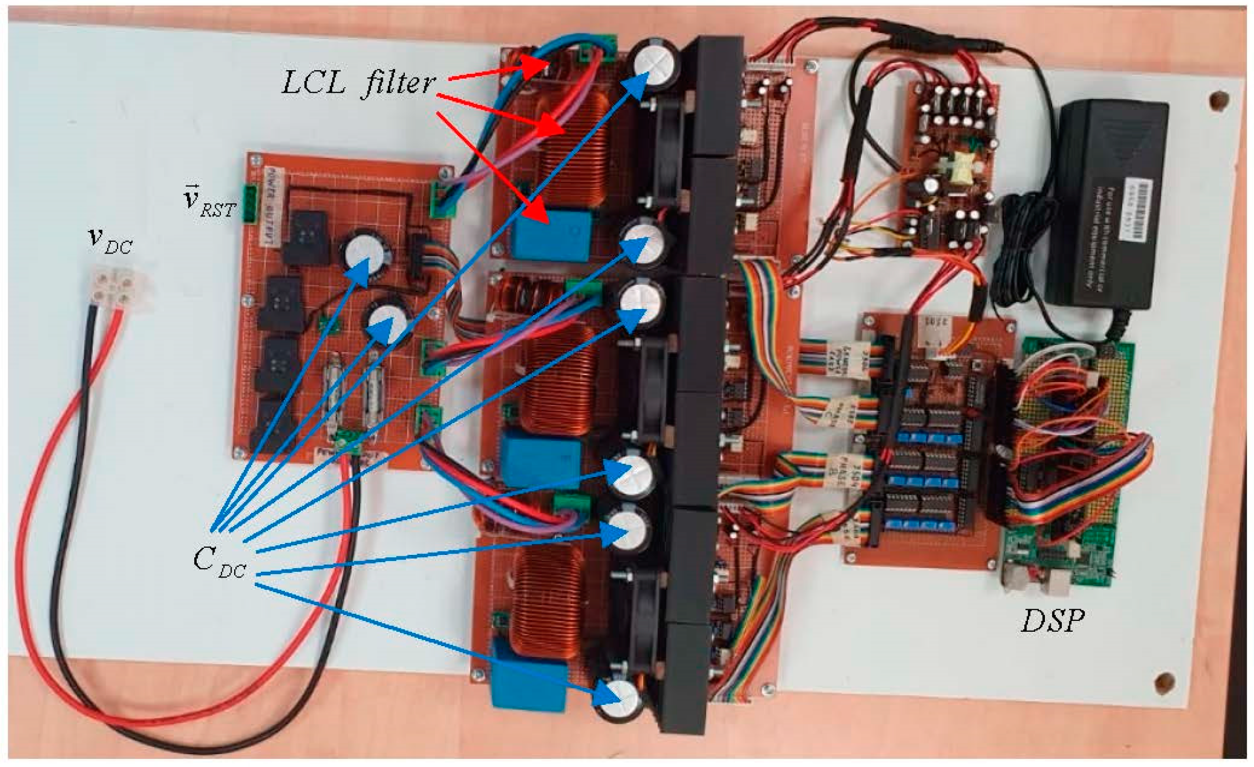
The corresponding experimental prototype shown in Figure 6 was built according to design guidelines in [38]. The converter was operated at 50 kHz switching/sampling frequency by a Texas Instruments TMS320F28335 DSP Control Card. The power stage was fed by a DC power supply and terminated by a three-phase balanced resistive load, drawing nominal power for a phase voltages magnitude of VM = 230 2 V ≈ 325 V. Four parallel connected 110 μF electrolytic capacitors (yielding slightly higher capacitance than the analytically predicted value in order to account for ESR-imposed ripple) were employed to realize each split DC link capacitance (i.e., eight devices in total were used, as seen in Figure 6). The system was simulated using PSIM software prior to conducting full-rating matching experiments. During the experiments, a 4-channel oscilloscope was employed, hence the total DC link voltage in Figure 8 was estimated by partial DC link voltage summation using an oscilloscope Math function.
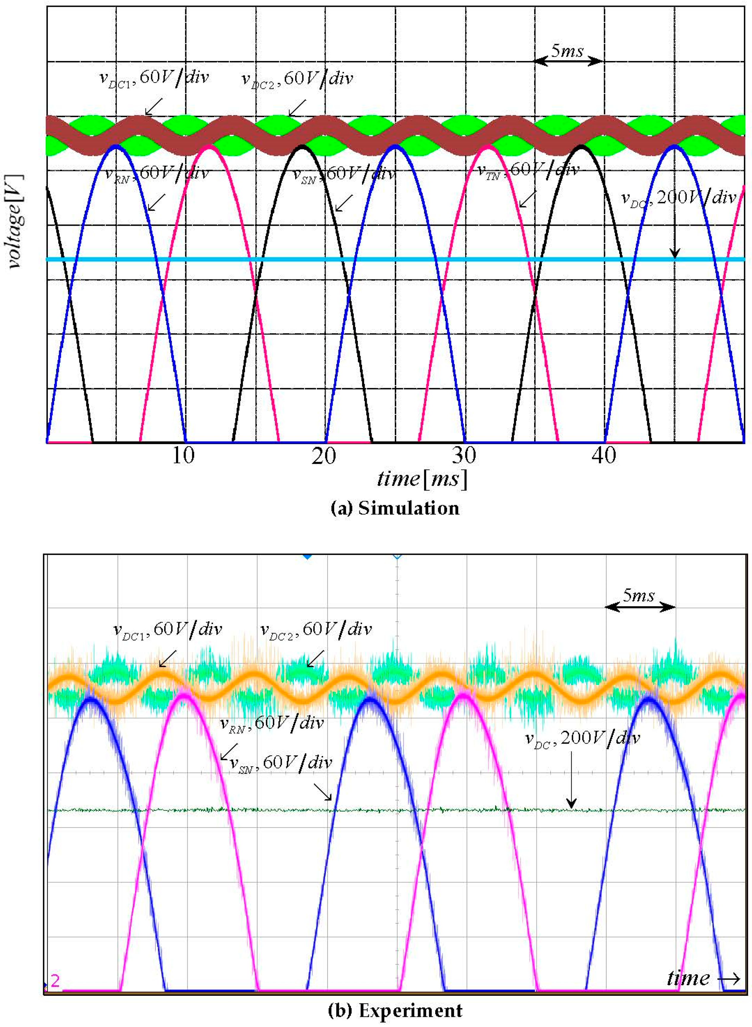
Simulated and experimental grid-side phase voltages and currents are depicted in Figure 7. It is well-evident that the system operates with unity power factor and under rated loading. Partial DC link voltages and grid-side phase voltage waveforms are shown in Figure 8. It may be concluded that the instantaneous values of partial DC link voltages are never below their grid-side phase voltages counterparts even though the global minimums of the former are below the global maximum of the latter, as expected.

4. Conclusions

The study introduces a methodology for ascertaining the minimum split DC link capacitance values in three-phase three-level DC-AC power converters that operate with unity power factor and do not involve AC zero-sequence component injection or supplementary balancing circuitry. The proposed approach relies on the tangency between partial DC link voltages and the absolute values of AC-side voltages as the boundary case to ensure appropriate power stage operation. It was shown that the proposed methodology allows for a two-fold reduction of utilized DC link capacitance compared to the previously proposed technique for the same value of the DC link voltage set point. The validity of the proposed methodology is reinforced by 10 kVA T-type converter simulations and experimental results that exhibit excellent correspondence.

Author Contributions

Conceptualization, D.B. and A.K.; methodology, Y.S. and A.K.; software, Y.S.; validation, Y.S., M.S., I.A. and S.L.; formal analysis, A.K.; investigation, Y.S.; resources A.K.; data curation, Y.S.; writing—original draft preparation, D.B.; writing—review and editing, M.S., I.A., S.L. and A.K.; visualization, Y.S., M.S., I.A. and S.L.; supervision, D.B., M.S., I.A., S.L. and A.K.; project administration, A.K.; funding acquisition, A.K. All authors have read and agreed to the published version of the manuscript.

Funding

This research was funded by the Israel Science Foundation under grant 2186/19, and by the Israel Ministry of Energy.

Data Availability Statement

Not applicable.

Conflicts of Interest

The authors declare no conflict of interest.

References

  1. Gazafrudi, S.; Langerudy, A.; Fuchs, E.; Al-Haddad, K. Power quality issues in railway electrification: A comprehensive perspective. IEEE Trans. Ind. Electron. 2015, 62, 3081–3090. [Google Scholar] [CrossRef]
  2. Taul, M.G.; Wang, X.; Davari, P.; Blaabjerg, F. Current reference generation based on next-generation grid code requirements of grid-tied converters during asymmetrical faults. IEEE J. Emerg. Sel. Top. Power Electron. 2020, 8, 3784–3797. [Google Scholar] [CrossRef]
  3. Singh, B.; Singh, B.N.; Chandra, A.; Al-Haddad, K.; Pandey, A.; Kothari, D.P. A review of three-phase improved power quality AC-DC converters. IEEE Trans. Ind. Electron. 2004, 51, 641–660. [Google Scholar] [CrossRef]
  4. Mellincovsky, M.; Yuhimenko, V.; Peretz, M.M.; Kuperman, A. Low-frequency DC-link ripple elimination in power converters with reduced capacitance by multiresonant direct voltage regulation. IEEE Trans. Ind. Electron. 2017, 64, 2015–2023. [Google Scholar] [CrossRef]
  5. Mutovkin, A.; Mellincovsky, M.; Yuhimenko, V.; Schacham, S.; Kuperman, A. Conditions for direct applicability of electronic capacitors to dual-stage grid-connected power conversion systems. IEEE J. Emerg. Sel. Top. Power Electron. 2019, 7, 1805–1814. [Google Scholar] [CrossRef]
  6. Baek, J.; Lee, J.-B.; Kim, J.-K. Effective hold-up time extension method using fan control in server power systems. IEEE Trans. Ind. Electron. 2020, 67, 5820–5824. [Google Scholar] [CrossRef]
  7. Huai, W.; Blaabjerg, F. Reliability of capacitors for DC-link applications in power electronic converters—An overview. IEEE Trans. Ind. Appl. 2014, 50, 3569–3578. [Google Scholar]
  8. Wang, H.; Wang, H.; Zhu, G.; Blaabjerg, F. An overview of capacitive DC links: Topology derivation and scalability analysis. IEEE Trans. Power Electron. 2019, 35, 1805–1829. [Google Scholar] [CrossRef]
  9. Wang, H.; Wang, H. Capacitive DC links in power electronic systems—Reliability and circuit design. Chin. J. Electr. Eng. 2018, 4, 29–36. [Google Scholar]
  10. Mutovkin, A.; Yuhimenko, V.; Schacham, S.; Kuperman, A. Simple and straightforward realization of an electronic capacitor. Electron. Lett. 2019, 55, 220–222. [Google Scholar] [CrossRef]
  11. Mutovkin, A.; Yuhimenko, V.; Mellinkovsky, M.; Schacham, S.; Kuperman, A. Control of direct voltage regulated active DC-link capacitance reduction circuits to allow plug-and-play operation. IEEE Trans. Ind. Electron. 2019, 66, 6527–6537. [Google Scholar] [CrossRef]
  12. Mutovkin, A.; Yuhimenko, V.; Schacham, S.; Kuperman, A. Nonlinear control of electronic capacitor for enhanced stability and dynamic response. IEEE Trans. Ind. Electron. 2021, 68, 6881–6892. [Google Scholar] [CrossRef]
  13. Lamar, D.G.; Sebastian, J.; Arias, M.; Fernandez, A. On the limit of the output capacitor reduction in power factor correctors by distorting the line input current. IEEE Trans. Power Electron. 2012, 27, 1168–1176. [Google Scholar] [CrossRef]
  14. Hanson, A.J.; Martin, A.F.; Perreault, D.J. Energy and size reduction of grid-interfaced energy buffers through line waveform control. IEEE Trans. Power Electron. 2019, 34, 11442–11453. [Google Scholar] [CrossRef]
  15. Marcos-Pastor, A.; Vidal-Idiarte, E.; Cid-Pastor, A.; Martinez-Salamero, L. Minimum DC-link capacitance for single-phase applications with power factor correction. IEEE Trans. Ind. Electron. 2020, 67, 5204–5208. [Google Scholar] [CrossRef]
  16. Strajnikov, P.; Kuperman, A. On the minimum DC link capacitance in practical PFC rectifiers considering THD requirements and load transients. IEEE Trans. Ind. Electron. 2022, 69, 11067–11075. [Google Scholar] [CrossRef]
  17. Krein, P.T.; Balog, R.S.; Mirjafari, M. Minimum energy and capacitance requirements for single-phase inverters and rectifiers using a ripple port. IEEE Trans. Power Electron. 2012, 27, 4690–4698. [Google Scholar] [CrossRef]
  18. Strajnikov, P.; Kuperman, A. DC link capacitance reduction in PFC rectifiers employing PI+Notch voltage controllers. IEEE Trans. Power Electron. 2023, 38, 977–986. [Google Scholar] [CrossRef]
  19. Erickson, R.W.; Maksimovic, D. Fundamentals of Power Electronics; Springer: New York, NY, USA, 2001. [Google Scholar]
  20. Malesani, L.; Rossetto, L.; Tenti, P.; Tomasin, P. AC/DC/AC PWM converter with reduced energy storage in the DC link. IEEE Trans. Ind. Appl. 1995, 31, 287–292. [Google Scholar] [CrossRef]
  21. Messo, T.; Jokipii, J.; Puukko, J.; Suntio, T. Determining the value of DC-link capacitance to ensure stable operation of a three-phase photovoltaic inverter. IEEE Trans. Power Electron. 2014, 29, 665–673. [Google Scholar] [CrossRef]
  22. Stecca, M.; Soeiro, T.B.; Elizondo, L.R.; Bauer, P.; Palensky, P. Comparison of two and three-level DC-AC converters for a 100 kW battery energy storage system. In Proceedings of the 2020 IEEE 29th International Symposium on Industrial Electronics (ISIE), Delft, The Netherlands, 17–19 June 2020; pp. 677–682. [Google Scholar]
  23. Tehrani, K.A.; Rasoanarivo, I.; Andriatsioharana, H.; Sargos, F.M. A new multilevel inverter model NP without clamping diodes. In Proceedings of the 2008 34th Annual Conference of IEEE Industrial Electronics, Orlando, FL, USA, 10–13 November 2008; pp. 466–472. [Google Scholar]
  24. Debnath, T.; Gopakumar, K.; Umanand, L.; Zielinski, D.; Rajashekara, K. A nine-level inverter with single DC link and low-voltage capacitors as stacked voltage sources with capacitor voltage control irrespective of load power factor. IEEE Open J. Ind. Electron. Soc. 2022, 3, 522–536. [Google Scholar] [CrossRef]
  25. Song, Q.; Liu, W.; Yu, Q.; Xie, X.; Wang, Z. A neutral-point potential balancing algorithm for three-level NPC inverters using analytically injected zero-sequence voltage. In Proceedings of the APEC ’03, Eighteenth Annual IEEE Applied Power Electronics Conference and Exposition, 2003, Miami Beach, FL, USA, 9–13 February 2003; pp. 228–233. [Google Scholar]
  26. Pou, J.; Zaragoza, J.; Rodriguez, P.; Ceballos, S.; Sala, V.M.; Burgos, R.P.; Boroyevich, D. Fast-processing modulation strategy for the neutral-point-clamped converter with total elimination of low-frequency voltage oscillations in the neutral point. IEEE Trans. Ind. Electron. 2007, 54, 2288–2294. [Google Scholar] [CrossRef]
  27. Alemi, P.; Jeung, Y.-C.; Lee, D.-C. DC-link capacitance minimization in T-type three-level AC/DC/AC PWM converters. IEEE Trans. Ind. Electron. 2015, 62, 1382–1391. [Google Scholar] [CrossRef]
  28. Sangwongwanich, A.; Novak, M.; Sangwongwanich, S.; Blaabjerg, F. Reliability of DC-link capacitors in three-level NPC inverters under different PWM methods. In Proceedings of the 2022 IEEE Applied Power Electronics Conference and Exposition (APEC), Houston, TX, USA, 20–24 March 2022; pp. 1804–1811. [Google Scholar]
  29. Srinivas, V.L.; Singh, B.; Mishra, S. Enhanced power quality PV inverter with leakage current suppression for three-phase SECS. IEEE Trans. Ind. Electron. 2022, 69, 5756–5767. [Google Scholar] [CrossRef]
  30. Zielinski, C.; Stefanczak, B.; Jedrus, K. Phase-independent reactive power compensation based on four-wire power converter in the presence of angular asymmetry between voltage vectors. Energies 2022, 15, 497. [Google Scholar] [CrossRef]
  31. Cao, D.P.; Song, W.X.; Xi, H.; Chen, G.C.; Chen, C. Research on zero-sequence signal of space-vector modulation for three-level neutral-point-clamped inverter based on vector diagram partition. In Proceedings of the 2009 IEEE 6th International Power Electronics and Motion Control Conference, Wuhan, China, 17–20 May 2009; pp. 1435–1439. [Google Scholar]
  32. Siton, Y.; Yuhimenko, V.; Baimel, D.; Kuperman, A. Baseline for split DC-link design in three-phase three-level converters operating with unity power factor based on low-frequency partial voltage oscillations. Machines 2022, 10, 722. [Google Scholar] [CrossRef]
  33. Schechter, N.; Kuperman, A. Zero-sequence manipulation to maintain correct operation of NPC-PFC rectifier upon neutral line disconnection and reconnection. IEEE Trans. Ind. Electron. 2017, 61, 866–872. [Google Scholar] [CrossRef]
  34. Kolar, J.W.; Friedli, T. The essence of three-phase PFC rectifier systems—Part I. IEEE Trans. Power Electron. 2013, 28, 176–198. [Google Scholar] [CrossRef]
  35. Friedli, T.; Hartmann, M.; Kolar, J.W. The essence of three-phase PFC rectifier systems—Part II. IEEE Trans. Power Electron. 2014, 29, 543–560. [Google Scholar] [CrossRef]
  36. Gadelovits, S.; Kuperman, A. Modeling and classical control of unidirectional VIENNA rectifiers. In Proceedings of the 2012 Electric Power Quality and Supply Reliability, Tartu, Estonia, 11–13 June 2012; pp. 1–4. [Google Scholar]
  37. Singer, S.; Erickson, R.W. Power-source element and its properties. IEEE Proc. Circ. Dev. Syst. 1994, 141, 220–226. [Google Scholar] [CrossRef]
  38. Available online: https://www.ti.com/lit/ug/tidue53f/tidue53f.pdf (accessed on 13 March 2023).
Figure 1. Generalized three-phase three-level grid-connected AC/DC power conversion system.
Electronics 12 01994 g001
Figure 2. Boundary condition of tangency between partial DC link and grid phase voltages.
Electronics 12 01994 g002
Figure 3. T-type three-phase three-level power converter.
Electronics 12 01994 g003
Figure 4. Graphical solution of (14) and (23) to obtain (24).
Electronics 12 01994 g004
Figure 5. Generation of zero-sequence component m0.
Electronics 12 01994 g005
Figure 6. Experimental prototype.
Electronics 12 01994 g006
Figure 7. Mains voltages and currents under rating loading.
Electronics 12 01994 g007
Figure 8. AC-side and DC-link side voltages under rating loading.
Electronics 12 01994 g008
Table 1. System parameter values.
ParameterValueUnits
VM 230 2 V
ω 2 π · 50 rad/s
Lf1 350 μH
Cf 10 μF
Lf2 10 μH
ESR(Lf1) 50
ESR(Cf) 316
ESR(Lf2) 1
PL 10 kW
VR 360 V
α0.97-
Disclaimer/Publisher’s Note: The statements, opinions and data contained in all publications are solely those of the individual author(s) and contributor(s) and not of MDPI and/or the editor(s). MDPI and/or the editor(s) disclaim responsibility for any injury to people or property resulting from any ideas, methods, instructions or products referred to in the content.