Review

An Overview of Multilevel Inverters Lifetime Assessment for Grid-Connected Solar Photovoltaic Applications

by
Shaik Nyamathulla
1,
Dhanamjayulu Chittathuru
1,* and
S. M. Muyeen
2,3,*
1
School of Electrical Engineering, Vellore Institute of Technology, Vellore 632014, Tamil Nadu, India
2
School of Electrical Engineering, Component and Mathematical Sciences, Curtin University, Perth, WA 1987, Australia
3
Department of Electrical Engineering, Qatar University, Doha 2713, Qatar
*
Authors to whom correspondence should be addressed.
Electronics 2023, 12(8), 1944; https://doi.org/10.3390/electronics12081944
Submission received: 27 February 2023 / Revised: 7 April 2023 / Accepted: 18 April 2023 / Published: 20 April 2023
(This article belongs to the Special Issue Feature Papers in Industrial Electronics)

Abstract

:
Nowadays, due to advancements in power electronic devices as well as the rise in consumer awareness of the need to protect the environment on a global scale, many people are turning to the use of solar photovoltaic (PV) technology in the distributed power generation side. In the field of power electronics, manufacturers need to develop products that have high lifespans. Power electronic device reliability is important for the maintenance of the device and may be scheduled under that information. Rather than preventing failures, reliability can be improved by predicting them. Even though some research has been conducted over the past few years to investigate the reliability of power electronic devices, the reliability is many common circuits has not been investigated and this leads to a big challenge for researchers. In this review paper, an overview of the grid-connected multilevel inverters for PV systems with motivational factors, features, assessment parameters, topologies, modulation schemes of the multilevel inverter, and the selection process for specific applications are presented. In this paper, the findings of a comprehensive reliability analysis of fundamental multilevel inverters are studied. To evaluate the reliability of three basic multilevel inverters, a calculation is made using each component’s mean time before its failure. Two techniques of computation approximate and exact were used to arrive at the final result. To calculate power losses in temperature-sensitive components such as diodes and switches, MATLAB Simulink is employed. In addition, the concept of oversizing photovoltaic (PV) arrays is presented in this study. This concept proposes that energy output may be increased by increasing the size of the PV array under conditions of poor solar irradiation. Finally, the mission-profile-based and Monte Carlo simulation-based methods process flows are discussed for the accurate lifetime prediction and reliability assessments of PV inverters in a real-time scenario, followed by a conclusion with future work.

1. Introduction

Energy demand from the power grid has grown dramatically over the previous decade due to an increase in users and high-power sectors. As a result, traditional power production has resulted in a huge increase in world emissions. Hence, the incorporation of solar and wind power into the electricity system has greatly grown. Photovoltaic (PV) systems are now the most preferred resource due to their tremendous potential. Hence, the globally grid-connected solar PV power generation has climbed to more than 635 GW, meeting roughly 2% of global energy consumption. According to the International Energy Agency (IEA), solar photovoltaic (PV) energy may offer 11% of total green energy globally, which equates to a significant decrease in CO2 emissions of 2.3 giga tons per year. The sun is the source of solar energy, delivering 1367 W/m2 to the atmosphere. The entire worldwide absorption of solar energy is almost 1.8 × 10¹¹ MW, which is sufficient to cover the world’s current electricity needs. Figure 1 shows that solar energy generating capacities have increased dramatically over the previous decade, and extrapolation shows that they might reach 1700 GW by 2030 [1].
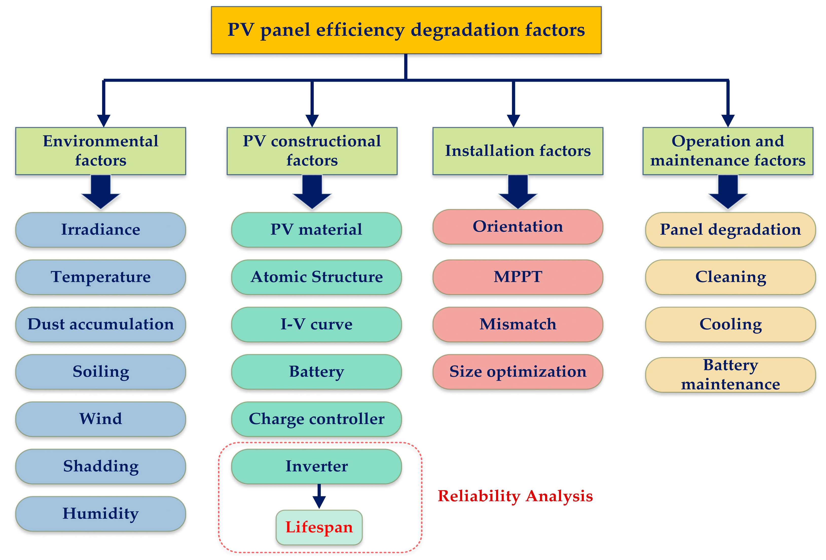
Several external and internal issues, including environmental, constructional, installation, operation, and maintenance issues, are to blame for the decline in PV panel efficiencies in Figure 2. However, PV construction components and installation methods will be progressively updated.
Solar panels produce DC voltage, an inverter is needed to transform the solar power into usable AC power. The medium-voltage grids’ direct connection of AC voltage supplied by renewable sources is crucial in today’s business due to the demand for higher-power equipment. To deal with these larger input voltages and boost the output voltage, multiple inverters have been developed. Satellites also rely on solar cells as a reliable source of electrical power. An investigation was conducted to determine the most effective method of absorbing energy from photovoltaic (PV) modules mounted on an orbiting spacecraft. The reliability of the inverter and the PV module is crucial in a satellite feed system. It stands to reason that an inverter would last longer in service if it is more reliable. The initial efficiency of most PV modules is just around 25% [2], although their makers offer a 25-year lifespan, and multilevel inverters, widely regarded as the next generation of inverters, are thus receiving more attention as a means to solve the inverter reliability issues.
The MLI provides several inherent advantages over two-level inverters. This has led to the development of many new and exciting research advancements in the field of power electronics, such as multilevel inverters (MLIs) [3,4,5,6,7]. The MLIs’ ability to construct a stepwise output voltage waveform by combining numerous tiny voltage levels. The MLIs have less total harmonic distortion (THD), reduced stress on switches, a low di/dt effect, and less electromagnetic interference (EMI). References [3,4,5] are mentioned in Table 1.
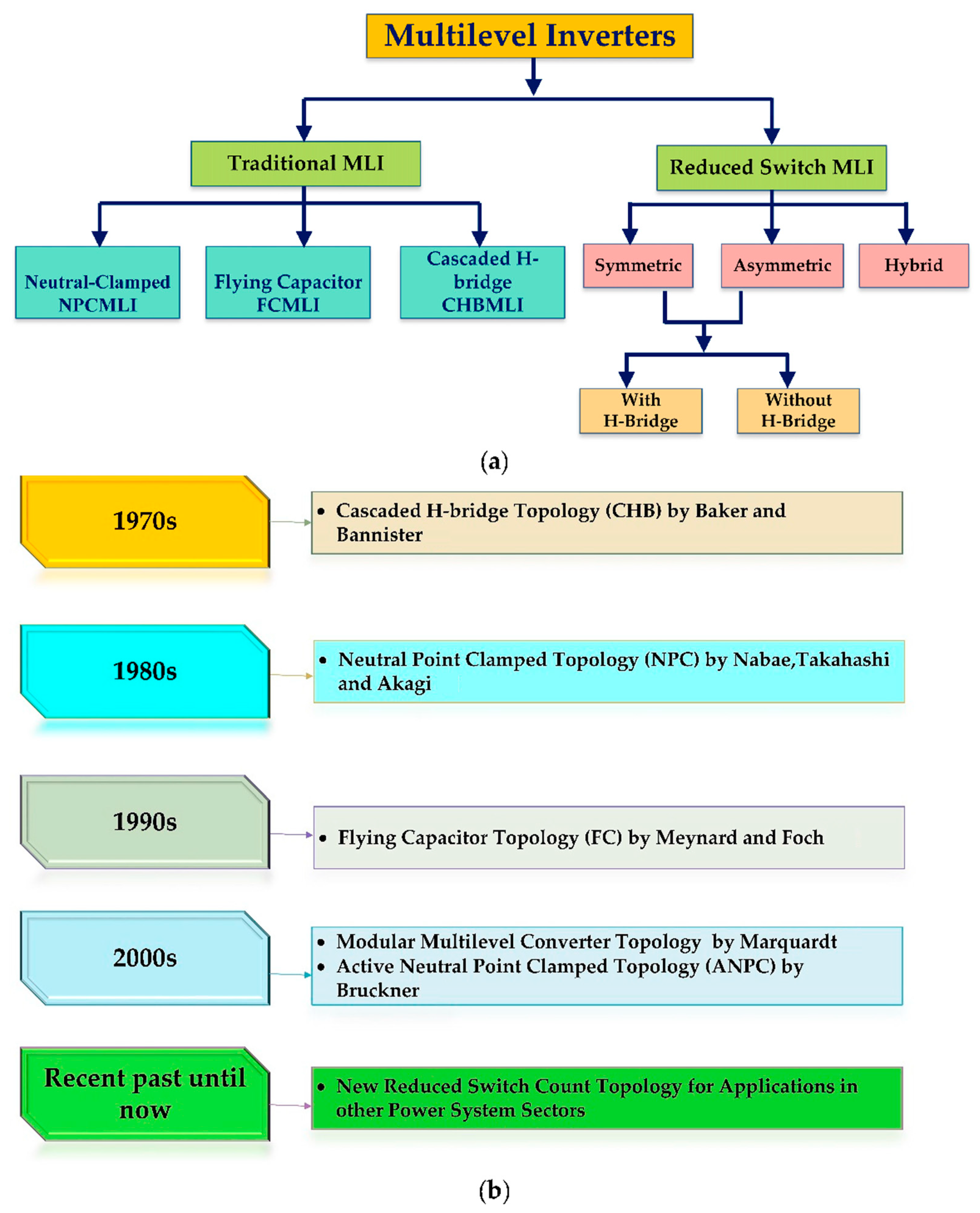
Multilevel inverters come in a variety of topologies and control approaches. In general, multilevel inverters are classified into two types: traditional and reduced switch types. Figure 3a,b show three standard topologies for multilevel inverters and their developments [8,9,10,11,12].
Although basic inverters have found widespread use in several sectors, there are still many unknowns regarding these topologies because of the unsolved advancements of the supplementary categories of converters. In recent years, a variety of innovative topologies have been developed to enhance performance, boost reliability, and decrease the number of circuit parts. In this article, we employed a three-level system with these three specified inverters, and the circuit diagrams of these inverters are shown in Figure 4.
This paper provides a thorough analysis of the idea of reliability and an evaluation of the dependability of multilevel inverters. Multilevel inverter dependability is determined using both approximate and exact methods. Assembling the reference failure rates for each component and using that total as an approximation is how we receive our approximation. The exact method provides a stress technique for assessing component reliability for inverter evaluation. For the first time, this research determines the reliability of fundamental multilevel inverters with a rigorous method that takes into consideration all possible scenarios.
The significant contributions of this review paper include:
The following is the outline for this paper. Section 2 outlines an overview of the grid-connected multilevel inverters for PV systems with motivational factors, features, assessment parameters, topologies, modulation schemes of the multilevel inverter, and the selection process for specific applications, and the common failure mechanisms of power electronic devices are discussed in great length. A comprehensive evaluation of the reliability of CHB, FC, and NPC using two approaches is presented in Section 3, and this section also explains the fundamental principle of reliability and the approximate and exact methods proposed for assessing the lifespan. In addition, this section illustrates the effect of series redundancies. Finally, in Section 4, the mission-profile-based and Monte Carlo simulation-based methods’ process flows are discussed for the accurate lifetime prediction and reliability assessment of a PV inverter in a real-time scenario, followed by a conclusion with future work.

2. Grid-Connected Power Electronic Devices and Failure Mechanisms: Background

The sun’s energy is converted into electricity using PV cells in solar-based technology. Photovoltaic cells, converters, and an energy control unit are depicted in Figure 5 of the system for solar energy conversion [13,14]. Despite this, more research is being done on how to integrate renewable sources of energy into the power system for greater efficiency. Due to their critical function in converting power and regulating output power, power converters and their controls are given increased attention in this respect. In most cases, renewable energy sources are integrated into the DC grid using DC–DC converters as the first step. The output voltage variability of non-conventional energy sources such as wind and photovoltaics (PV) necessitates a high efficiency at this step. Therefore, the DC–DC front-end stages must be able to react to this fluctuation so that they may work at their maximum efficiency. DC–DC converters change the voltage level of a direct current (DC) source. Low-to-high and vice versa. They also use high frequency switching modes, transformers, inductors, and capacitors to reduce switching noise (EMI) to a minimum, which is necessary for particular applications such as industrial, medical, railway, and RES power production. The DC–DC converter works by varying the input current via an inductor. Energizing the switch activates the inductor, which stores magnetic energy. Energizing the switch closes it. To calculate the time constant of an RC circuit, the capacitor output voltage is considered to be high enough. A constant output voltage Vo (t) = Vo (constant) is ensured at the load terminal by the enormous time constant.
These inverters are often used in small-scale industrial or utility applications because of their high voltage stress, poor efficiency, as well as their high operating temperatures and pressures. This is why large-scale, high-power, grid-connected renewable energy systems employ mostly multilevel inverters [15].

2.1. DC–AC Converters (or) Reduced Switch Multilevel Inverters (RSC-MLIs)

The goal of RSC-MLIs is to surpass the size and complexity restrictions of traditional MLIs. However, alterations in their topological organization have an impact on their structural and operational characteristics.

2.1.1. Motivational Factors

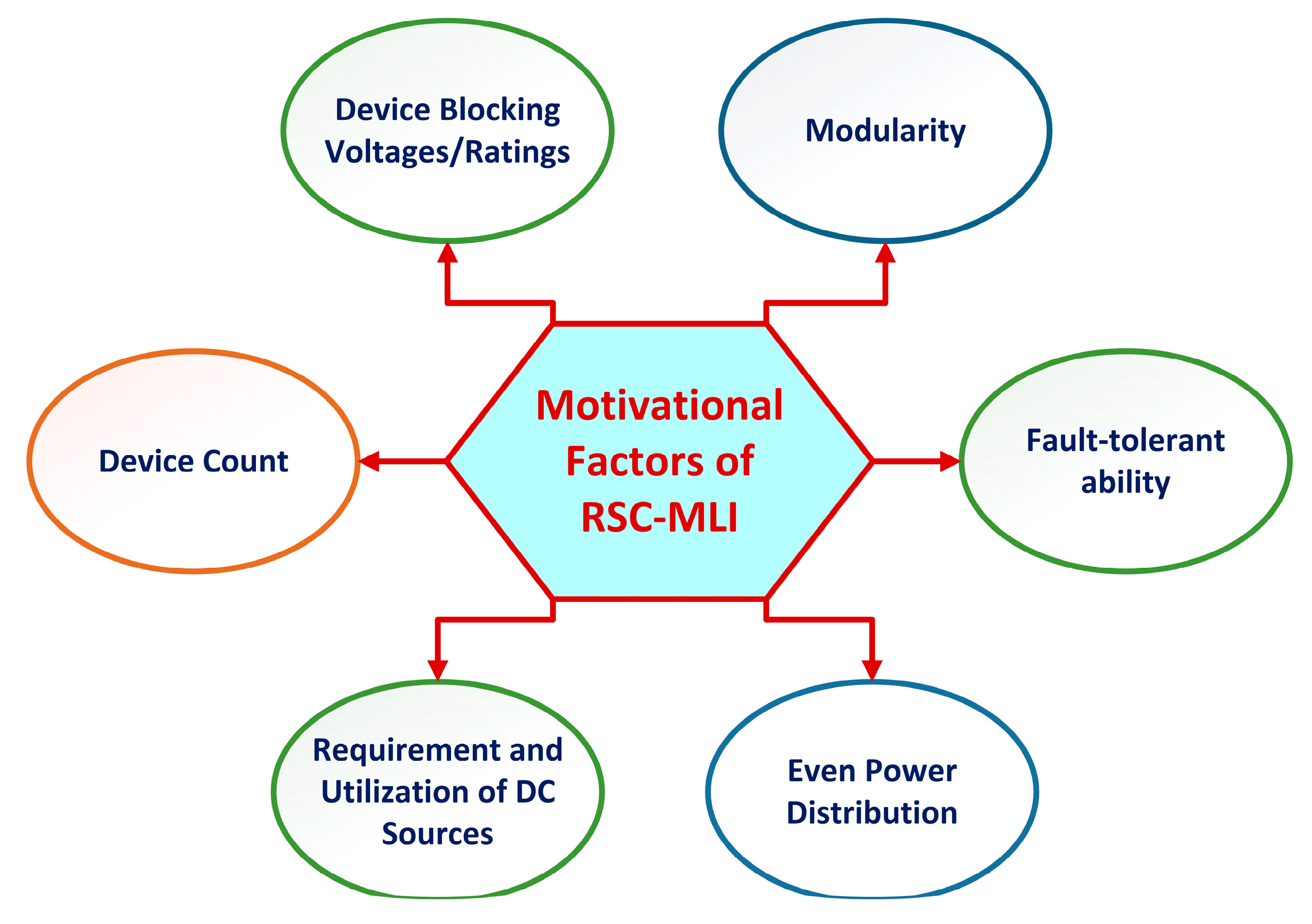
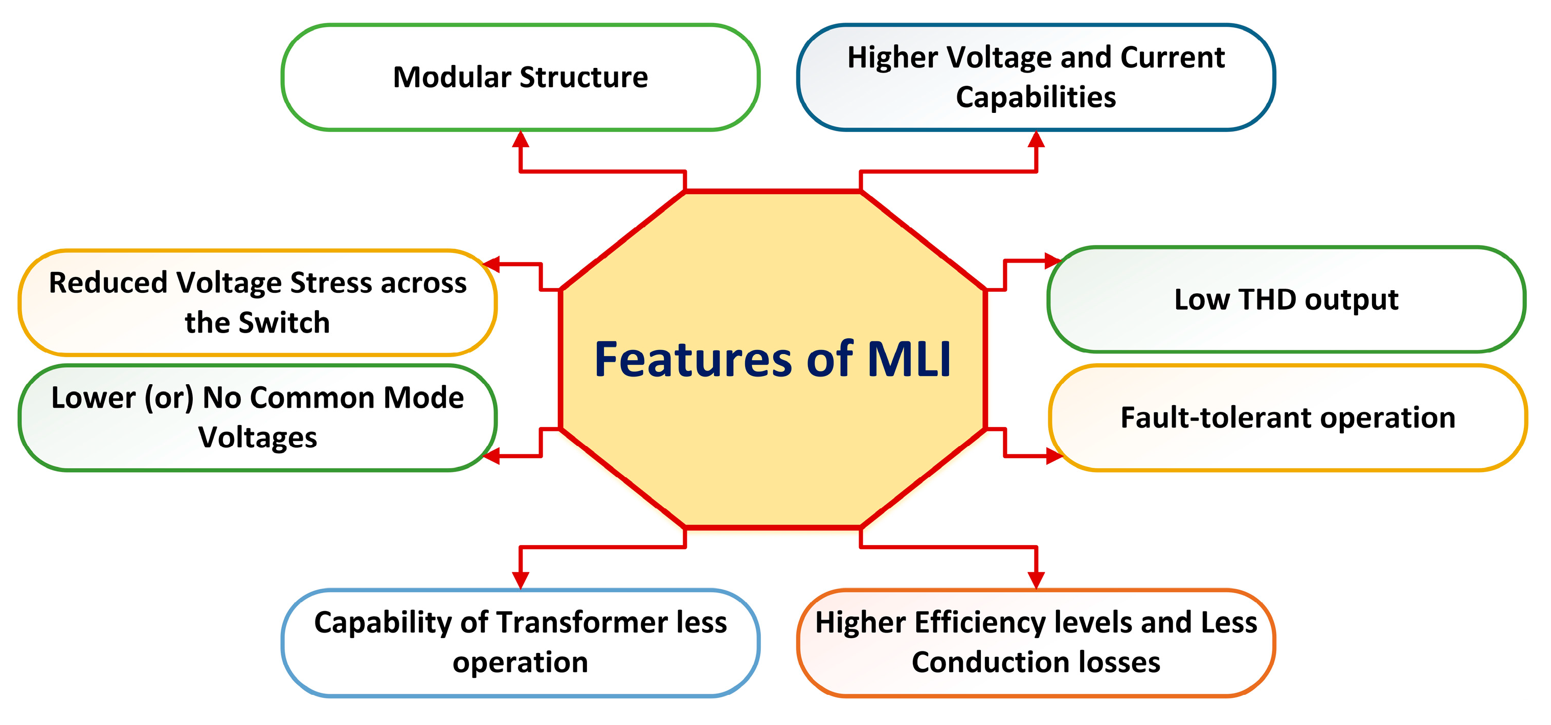
When constructing a novel RSC-MLI topology, researchers typically look at the following properties, as illustrated in Figure 6, as a possible rationale. The following is a list of the most important characteristics.

2.1.2. Classification

Devices such as switches and DC-link voltages may be coupled in any topology in any physical architecture. Including ladders, staircases, columns, U-shaped structures, and cascade structures, and, in certain cases, there is no specified architecture at all. As a result, based on their topological and operational characteristics, created RSC-MLIs may be classed as follows, as seen in Figure 7.

2.1.3. Assessment Parameters for MLI

However, in this study, generic criteria for the assessment of suggested topologies are considered:
In Figure 8, several assessing parameters of MLI are demonstrated to be dependent on these factors. Here are some of the MLI’s most important causes behind this ability, as demonstrated in Figure 9.
An interconnected multilevel converter system may practice renewable energy sources including solar PV, wind energy, and fuel cells. Their operation, effectiveness, improved power quality, and applications are mostly determined by the control scheme used in MLI PWM. Multiple MLI topologies have been suggested in recent years [16,17,18,19]. Based on the magnitude of DC sources, the MLIs are classified in Figure 10.

2.1.4. Modulation Techniques

Modulation schemes control inverter efficiency metrics including harmonic reduction and switching losses. They create reference control signals to balance voltage sources. Modulation generates a staircase DC voltage signal that matches a sinusoidal reference signal. Modulation generally comprises various carrier signal waveform properties with a modulating waveform. Modulation is a way to regulate switching by modifying the properties of a carrier signal with the reference signal. To select a suitable modulation scheme, total harmonics, distortion, switching frequency, losses, and reaction time factors are to be considered.
  • Sine Property: This is a contemporary technique for determining the firing angle to be supplied to the switching devices. By using this approach, calculating the firing angle is simple. To do simulations with ease, the firing angle is often calculated in degrees with the option of converting to any other unit of time, such as “seconds”.
  • Space Vector/Nearest Vector Control (SVC/NVC): This operates at a low switching frequency and is an SHE alternative. It does not generate the average load voltage for every switching time such as SHE. SVC selects a vector closest to the reference vector to minimize the distance or space error. The NVC approach is straightforward and appropriate for greater output voltage levels, since the increasing density of vectors generates only modest mistakes concerning the reference vector.
  • Selective Harmonic Elimination (SHE): In 1973, researchers proposed SHE, a voltage control and harmonic elimination theory. This method eliminates the most dominating chosen lower-order harmonics. SHE can reduce output filter size and THD. As the switching angles are pre-determined as offline, it is presumed to be open-loop modulation. The firing angle for switching is calculated using multiple Fourier equations, according to the authors. By choosing the firing angle for the Fourier series equation correctly, odd harmonics may be restricted for any MLI level. These firing angles are sent to switches via a microcontroller. Hence, it may be implemented without a closed-loop controller.
High-Frequency Switching Pulse Width Modulation is used for high switching frequencies (kHz) and numerous commutations per cycle.
  • Multi-Carrier Pulse Width Modulation (MC-PWM) technique: This method uses numerous triangular carriers to generate a single modulating sinusoidal signal. The number of carriers is usually (n−1), where n is the inverter level. Carrier disposition PWM and phase-shifted PWM are two forms of MC-PWM.
  • Space Vector Pulse Width Modulation (SV-PWM) technique: The reference waveform is modulated by numerous vector states in the SV-PWM approach. This approach generates PWM voltages under a known voltage using digital modulation. This system fails with several levels because sector identification and switching sequence selection are critical. An “n”-level inverter needs “(n − 1)2” vector combinations per sector, six sectors, and “n3” switching sequences. This approach achieves a better fundamental voltage ratio and better harmonic removal than sinusoidal PWM. SV-PWM also has a 15% higher maximum peak output voltage than triangle carrier-based modulation.

2.2. Applications of Multilevel Inverters in Renewable Energy Systems

2.2.1. Solar Photovoltaic (PV) Systems

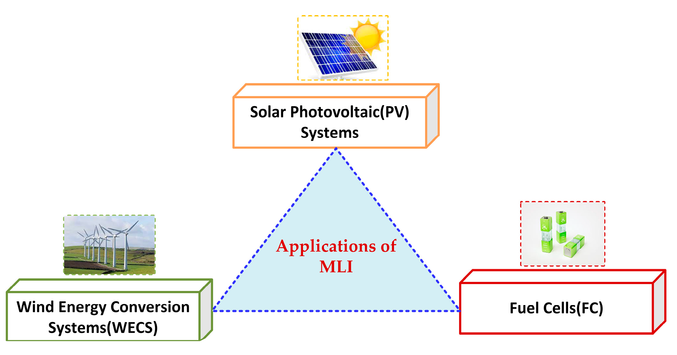
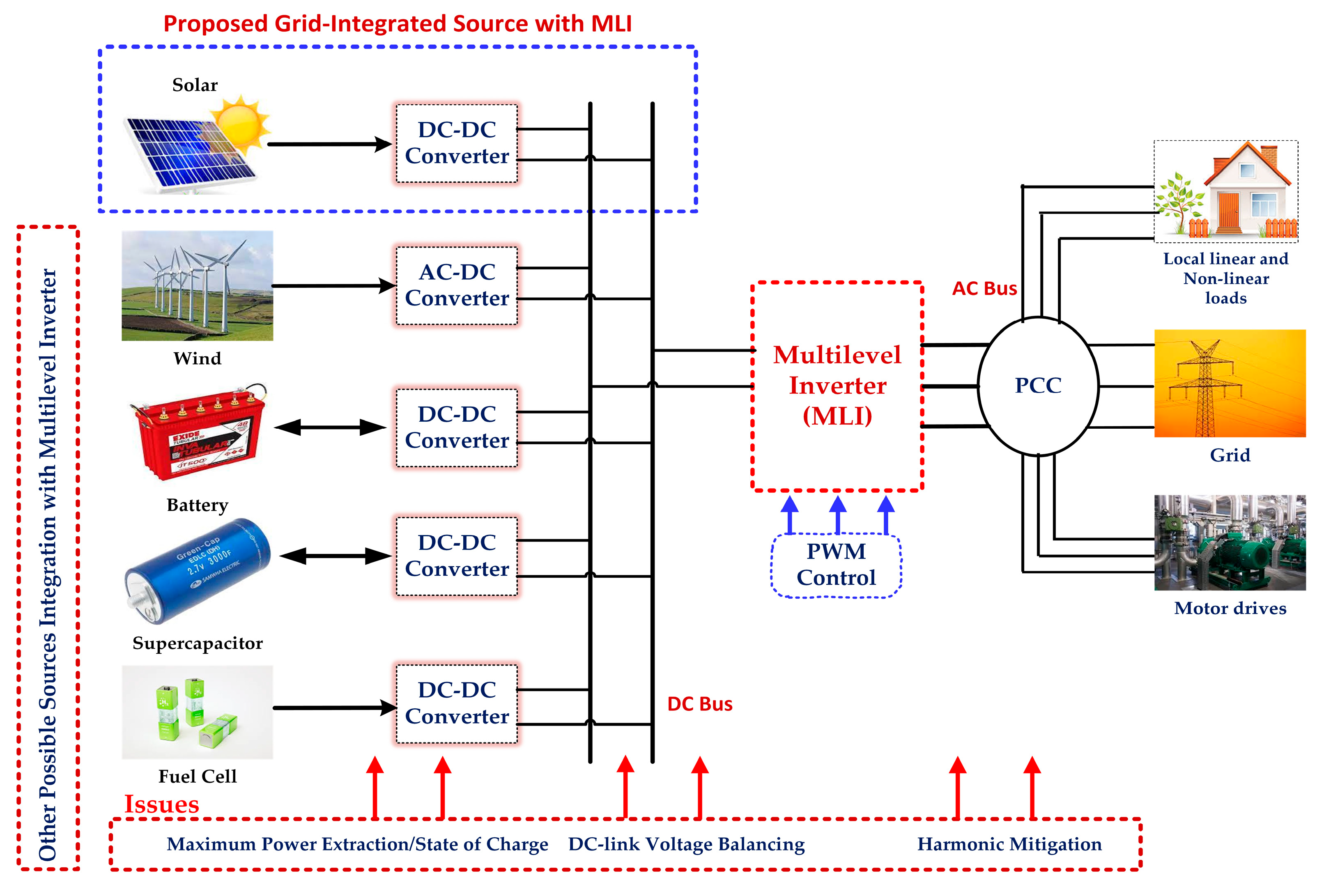
The use of multilevel inverters (MLIs) in solar PV systems increases power quality and efficiency. An important problem in photovoltaic (PV) system designs is determining the best converter for each application. The MLI is chosen for medium- and high-power applications due to its ability to produce high-quality voltage waveforms while operating at a low switching frequency [20,21,22]. Figure 11 exhibits examples of MLIs being employed in diverse applications, and Figure 12 illustrates the different possible types of energy sources integrated with MLI-based systems.

2.2.2. Wind Energy Conversion Systems (WECS)

An effort was made to connect split winding wind alternators (SWAs) to the power grid using CHBMLI topology. The results from the experiments with the SWA-CHBMLI system showed that it was effective for interfacing a large wind turbine to the grid, and it also improved power quality at the PCC. Recent years have seen an increased scholarly focus on designs for MLIs that used fewer gate drivers and switches to decrease both the amount of space needed for installation and the cost of MLIs. Wind turbine grid integration has been studied using a modular-cascaded MLI in a fault-tolerant distributed control system. After resolving a grid fault or upon first connection to the grid, the inverter was found to be able to synchronize with grid frequency without causing any harm to the incoming currents.

2.2.3. Fuel Cells (FC)

The variable-frequency-inverted sine wave carrier modulation approach is devised and constructed as a hybrid-cascaded MLI for use in fuel cells (VFISPWM). The output voltage is optimized with this modulation method for minimal THD and low switching losses. Fuel cell power conditioning systems may benefit from a hybrid-cascaded multilevel inverter CMLI. The designed system can generate high voltages at rapid speeds with high conversion efficiencies and minimal switching losses. The developed technology applies to high-output fuel-cell setups.

2.3. Failure Mechanisms of Modern Power Electronic Devices

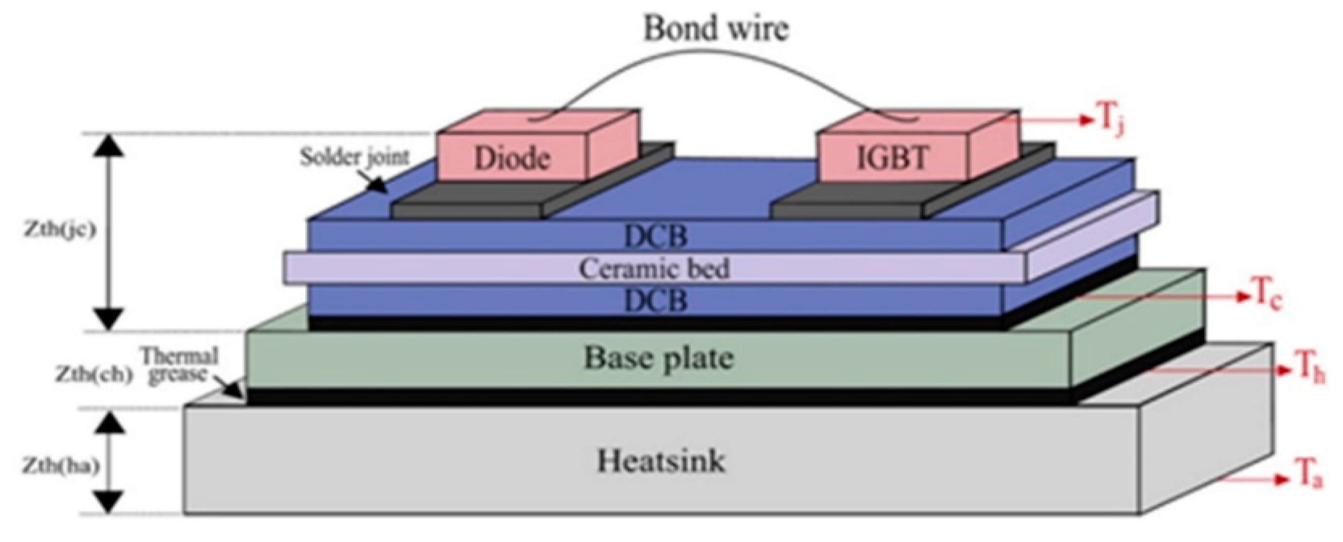
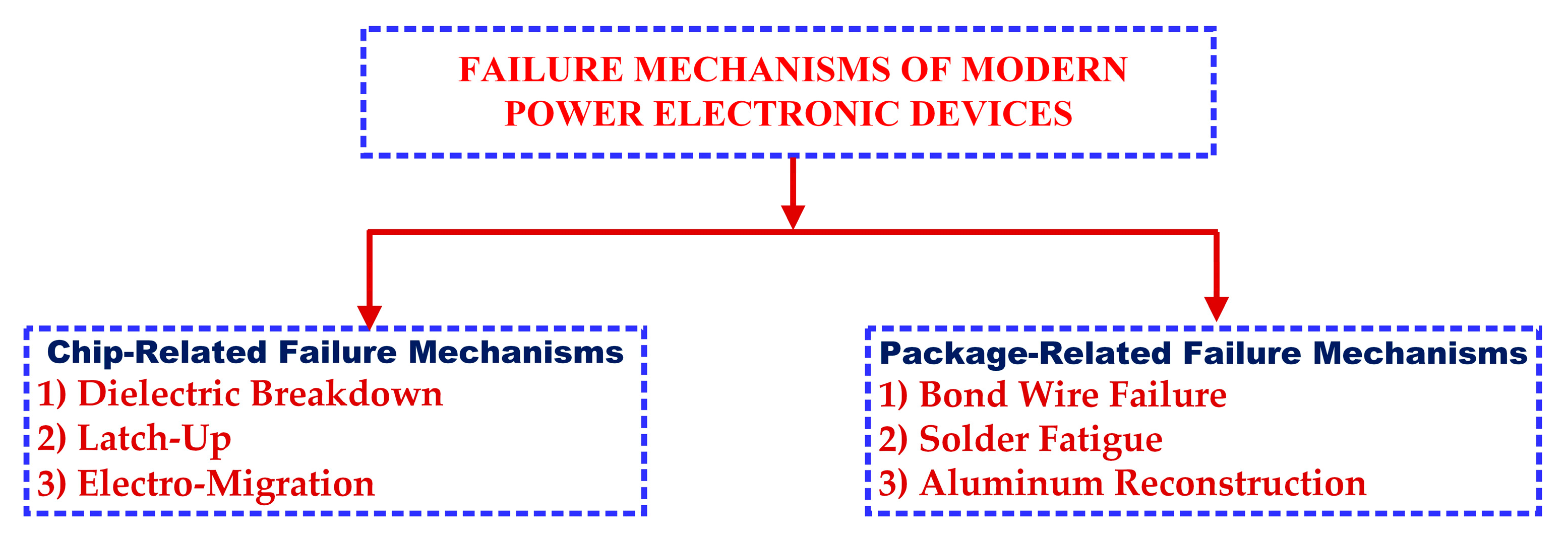
Power electronic devices may be broken down into two categories: discrete devices and power electronic modules. Thermal, chemical, electrical, and mechanical stresses all contribute to the continuous degradation and eventual collapse of these power electronic equipment as shown in Figure 13. In the case of hybrid electric cars, heat damage is the leading cause of breakdown [23]. Additionally, stress or vibration might speed up the deterioration process. Earlier research divided power electronic device failure mechanisms into two classes: those that occurred on the chip itself (intrinsic failures), and those that occurred in the package (extrinsic failures) [24,25]. Extrinsic failures are often generated by thermal–mechanical overstress, but intrinsic failure mechanisms are typically associated with electrical overstress, namely, high current and high voltage.
The incompatibility of the materials’ coefficients of thermal expansion (CTE) is the root cause of failure in packaging. It should be noted that the failure mechanisms discussed here are not an exhaustive list. This section’s primary goal is to lay the groundwork for reading the rest of the article. For a more in-depth look at the underlying causes of failure in power electrical devices, see [24,26]. Many failure causes can be reduced or eliminated with the advent of new technologies such as die-to-attach and bond wire materials and improved Silicon carbide (SiC) power modules; however, these innovations are either in their infancy or may be prohibitively expensive [27,28]. Therefore, there are several flaws in SiC module wafers produced in factories. Since the electric field strength in a SiC MOSFET is nearly three-times greater than in similarly rated Si devices [29], the gate oxide layer is extremely fragile in these devices. Hence, it is expected that traditional power electronics will continue to rule the industry for the foreseeable future.

2.3.1. Chip-Related Failure Mechanisms

  • Dielectric Breakdown: The Failure Mechanisms of Contemporary Power Electronic Devices are listed in Figure 14. A time-dependent dielectric breakdown (TDDB) occurs when gate oxide degrades owing to accumulating faults [25,30]. Impact ionization, anode hole injection, and trap production are described in [31]. Catastrophic/acute dielectric breakdown happens when the device undergoes extreme electrical or thermal stress, such as overvoltage and electrostatic discharge [25,32].
  • Latch-Up: IGBTs and MOSFETs can latch up if the parasitic thyristor or bipolar junction transistor structure is activated, causing a loss of gate control. Any excessive current will kill the device if the latch-up is not eliminated [30,33]. High dv/dt causes MOSFET and IGBT latch-up. In [34], heating the IGBT caused a latch-up.
  • Electro-Migration: Metal migration from high current density in silicon interconnects [24,25,32]. Voids arise between metal connections, causing resistance or an open circuit. Large contact surfaces prevent power electronics from degrading [24].

2.3.2. Package-Related Failure Mechanisms

The failure mechanisms described here are in line with those found in high-power applications that use power modules. It’s worth noting that even low-power devices might be susceptible to these failure types. The layered power modules shown in Figure 13 can operate on several voltage levels. For electrical isolation, silicon chips are first attached via solder to a direct-bonded copper (DBC) substrate before being attached to a bottom plate. Connections between semiconductors and terminals are made by bond wires. Bond wire failure, solder fatigue, and aluminum rebuilding are all recognized as major failure mechanisms [26].
  • Bond Wire Failure: Bond wire failures are of two types: (1) Lift-off and (2) heel-cracking bond wire. Mismatching Si and Al CTEs causes bond wire lift-off. During thermal cycling (TC), a fracture forms at the wire-to-device contact, leading to bond wire lift-off. Bond wire heel cracking is caused by fracture fatigue. Thermal cycling alters a bond wire loop’s bending angle by shifting its top. Advanced IGBT modules seldom fatigue [26].
  • Solder Fatigue: A typical power module has two solder layers: one between the Si device and DBC and another between the substrate and baseplate in Figure 13. A higher substrate-to-baseplate CTE mismatch causes solder fatigue. Thermal and power cycling cause voids and fractures in solder-attached layers [35]. Void increases thermal resistance, raising die temperature and accelerating void propagation. Die temperatures and void growth generate a positive feedback loop. Heat might harm the gadget. Overheating can induce latch-up and failure to ON [36]. Package issues might cause chip issues.
  • Aluminum Reconstruction: Aluminum reconstruction is the aging of silicon chip metallization [37]. Aluminum can undergo reconstruction if compressive and tensile stresses exceed the elastic limit, brought about by the dissimilar CTEs of aluminum and silicon. This mode of failure is prevented by passivation layers [26]. A correlative table may be produced based on IGBT module failure modes and mechanisms to highlight likely failure sites, causes, and impacted parameters [38]. Table 2 summarizes, as follows.

3. Fundamentals of Reliability and Lifespan Evaluation

Manufacturers aim for maximum gadget efficiency. This optimal use comprises excellent output quality, longer longevity, less energy consumption, etc. Longer-lasting converters are more reliable. Reliability shows system failure probability [39]. To analyze a system’s dependability, it must be broken into smaller sections and evaluated individually. Reliability is judged by several factors. Figure 15 indicates a measure of system reliability [40].

3.1. Reliability

“The capacity of an object to execute the required function under the given conditions over a certain time period” [41] is the definition of reliability, which is often quantified by measuring the likelihood of a failure or the frequency with which it occurs. Figure 16 depicts the categories of reliability and how the typical distribution of system reliability can be done [42].
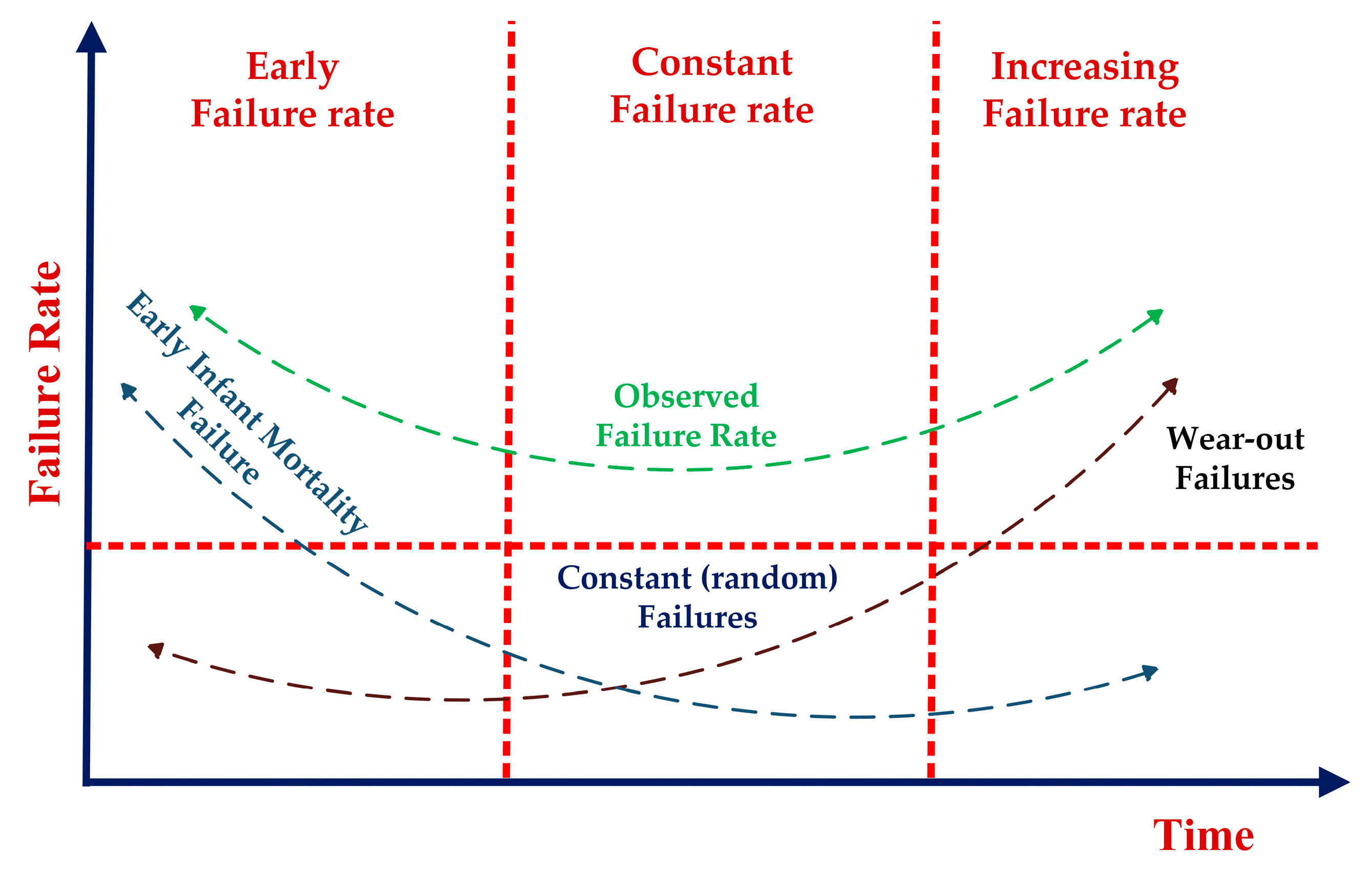
When studying the idea of dependability, researchers typically ignore the passage of time, which is especially important for industrial items that are covered by warranties [40]. There are three time points that may be used to illustrate a failure’s progression through time. In the beginning, you will be in a learning phase when your rate of job failure will gradually go down. The duration of this time frame might range from a few minutes to a few hours. Second, there is a random amount of time, known as the failure consolidation phase, which demonstrates that failure does not evolve following the learning phase. The third period is known as the fatigue stage, and it is characterized by a rise in failure rates with time. It is possible to construct a combined failure graph [42] by summing the three time intervals into a single one. The hazard function representation of this coupled graph is known as the bathtub curve graph (Figure 17). Similar to the merged graph, this one has three subsections [43]:
  • The burn-in or early failure period, during which the hazard function tends to diminish with time.
  • There is a constant danger function during the random failure.
  • The deterioration period, where the threat function rises.

3.2. Failure

Failure happens when, for any reason, the system stops doing the process that was asked of it. Thus, the amount of time that something works without breaking down is usually a random variable. There are two different kinds of failure: sudden and slow. Failure that happens all of a sudden is called “cataleptic failure”, and failure that happens over time is called “degradation failure” [44].

3.3. Failure Rate

When determining system reliability, the failure rate is a key factor. A definite time’s failure probability can be calculated using the “failure rate” function. It may be described as the likelihood of a failure occurring once every time unit throughout the interval [t, t + Δt], assuming no failures occurred before t. The following equation is used for calculating the failure rate [45]:
Failure rate = P (t ≤ T ≤ t + Δt|T > t)/(Δt) = P (t ≤ T ≤ t + Δt)/(Δt.P(T > t))
Here, P (t ≤ T ≤ t + ∆t) represents the chance that T will fail between time t and time t + Δt. The failure density functions CDF (f(t)) and PDF (f(t)) can be linked to probability:
P(t ≤ T ≤ t + Δt) = f(t)Δt = F(t + Δt) − F(t)
When all probabilities are added together (which would result in 1), the failure probability is subtracted, giving us the reliability probability distribution. Equation (3) gives us the dependability function of the constant hazard unit [46].
R (t) = 1 − F (t)
The failure density function offers the system dependability. Knowing component reliability allows for evaluating dependability. Exponential and Weibull functions are used to determine component reliability [45,46].
For Δt, it is common for t to be close to 0 or even smaller. Using [47], we receive the following Equation (4) representing the failure rate function:
z ( t ) = L i m Δ t 0 ( F ( t + Δ t ) F ( t ) Δ t · R ( t ) ) = f ( t ) / R ( t )
The proportion of attempts that fail is also represented by λ. The probability distribution function is derived from a mixture of the following failure rates using the Exponential distribution.
F (t, λ) = λ e−λt
The dependability function is obtained from Equation (6), as follows [35]:
R (t, λ) = e−λt
The failure in time (FIT) [40] is a metric for estimating the “failure rate” that is defined as the average number of failures per time interval.
1 FIT = 10−9 failure/hour

3.4. “Mean Time to Failure” (MTTF)

MTTF is the average time until a component or device fails once it begins working. This failure renders the gadget inoperable. MTTF is commonly given among parts specified in hours or thousand hours.
The reliability function used to define MTTF looks similar to this:
MTTF = 0 + R ( t )   d t
where e−λt is required to derive the reliability function. Consequently, the MTTF is expressed as follows [40,45,46,47]:
MTTF = 1 λ

3.5. “Mean Time to Repair” (MTTR)

“MTTR” is the amount of time it takes to fix broken equipment on average, and its worth is contingent on upkeep [17]. MTTR may be calculated using Equation (10), as follows, from [48], if we suppose that System X’s repair time follows a parametric gamma distribution.
MTTF = 0 + x   N ( x )   d t = β / µ
The N-Distribution of the “Gamma Function” (x) is N ( x ) . If we set equal 1 to β, the gamma distribution changes to an exponential one. Hence, 1/µ shows MTTR. MTTR is hard to quantify and is generally obtained experimentally [49].

3.6. “Mean Time between Failures” (MTBF)

MTBF is a significant quantitative indicator for achieving preventative maintenance and dependability. The MTBF is the average time between two consecutive failures. In References [50,51], the writers regarded have defended MTBF by saying it is a valid metric, since it adequately combines MTTR and MTTF readings. The following Equation (11) can be used to compute MTBF:
MTBF = MTTF + MTTR

3.7. “Availability” and “Average Availability”

“Availability” is used to describe the likelihood that a system will be operational at a given time. Equation (12) may be used to calculate the Typical Availability:
A avg = M T T F / ( M T T F + M T T R )

3.8. Methodology for Lifespan Evaluation

In 1956, the Rome Air Development Centre in the United States put out the first reliability estimation. It was called TR-1100. After this standard came out, this field’s most widely used handbook, MIL-HDBK-217, was released to the public. After that, companies and organizations began developing their own reliability manuals and applications, which were then refined over time. Here, some of the procedures are:
  • SAE’s PREL [52]
  • Siemens’ SN29500 standard [53]
  • CNET’s reliability prediction method [54]
  • RAC’s PRISM [55]
  • Telcordia SR-332 [56]
  • British Telecom’s HRD-4 [57]
In Reference [58], the writers compared the techniques for measuring dependability. Today, MIL-HDBK-217 is utilized to estimate dependability. As a military standard, MIL-HDBK-217 is more conservative than other standards. Moreover, this standard’s applicability compared to others has been shown due to its various and more features that cover all areas of dependability and influential things such as parts count and stress [59,60].

3.8.1. Approximate Technique

Two widely used methods quantify failure rates in reliability evaluations. First, count pieces to estimate a system’s dependability. This approach uses reference circumstances to forecast the failure rate. The actual operating circumstances will impact component count failure rates. This approach is approximate. In this strategy, only the number of components matters. This approach is quantitative.
The approximation method implemented here is analogous to the one utilized in Reference [61], which investigated the dependability of three-level “NPC” and “CHB” inverters based on “FIT”. In this paper, we focused on comparing the number of components and found that the “NPC” inverter was significantly more reliable than the “CHB” inverter by a factor of 4.5.
The voltage level of the analyzed inverters was clearly one of the parameters necessary for the analysis utilizing this approach. In truth, this way of comparison was identical to the components count approach, which estimates failure rates based on voltage values. Furthermore, the comparison was done when inverters were attached to the drive. As a result, a comparison without a drive is required.
First, we need to determine the inverter voltage, as was previously explained. The authors of [61,62] classified NPC, FC, and CHB inverters as high, high, and low voltage IGBT switches, respectively. The approach had consistently yielded a failure rate of 100 FIT for diodes, 400 FIT for high-voltage IGBTs, and 100 FIT for low-voltage IGBTs. It had also been shown that the failure rate of high voltage capacitors was 300 FIT, whereas that of low voltage capacitors was 400 FIT. The overall system failure rate may be calculated by multiplying the individual failure rates of the diodes, IGBTs, and capacitors by the total number of those components.
A device reference failure rate can be represented as:
λ sys = i = 1 N λ r e f ( i )   x   k
The total number of components (N) is multiplied by the reference failure rate λref (i) per element (k).

3.8.2. Exact Technique

The exact technique shows the components stress scheme. The parts stress technique involves knowledge of part stress levels and operating circumstances. To use this approach, the pressures on each item and exact environmental conditions must be known. Various pi factors in failure rate equations exhibit these situations. This method’s many factors make estimating failure rates hard, but they improve accuracy. Similar to the parts count approach, the parts stress method total failure rate is the sum of all failure rates. The next section reviews exact method relations. In MIL-HDBK-217, the circuit component failure rate is computed using the base failure rate. The base failure rate in Equation (14) is from [63]:
λ b = A .   exp   ( N T 273 + T + ( ( Δ T ) S ) ) ·   exp   (   273 + T + ( Δ T ) S T M )   P
Specifically, “A” is the scaling factor for the rate of failure. T is the temperature, and ΔT is the change in temperatures. “NT”, “TM”, and “P” are shape properties, and S is the stress ratio. The value of S is established by comparing the observed stress to the theoretical maximum.
MIL-HDBK-217 gives a combined technique to estimate dependability, determining each part’s reliability separately and as a whole. Form Equation (15) as per [64].
λp = λOπO + λeπe + λCπC + λSjπSj + λi
In this equation, λp is the expected failure rate, λO is the failure rate due to operational stresses, λe is the failure rate due to environmental stresses, λC is the failure rate due to temperature cycling stresses, λSj is the failure rate due to solder joints, and λi is the failure rate due to induced stresses.
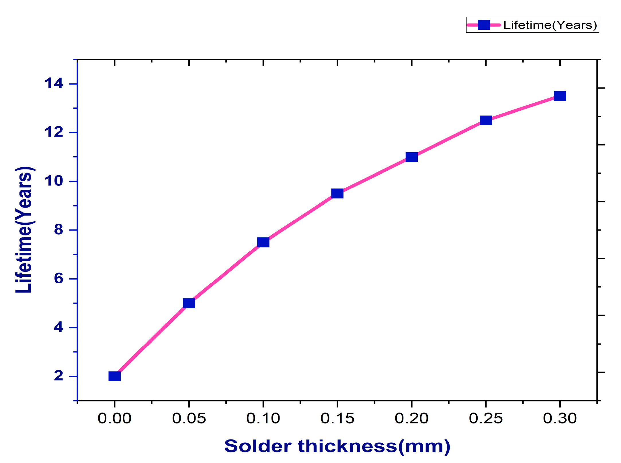
As the thickness of the solder rises, as does its dependability. Figure 18 depicts the influence of a solder junction on an IGBT module lifespan rises proportionally [65].
Research done recently on the reliability of electronic parts (switches, diodes, capacitors, inductors) provides correlations and formulas for predicting failure rates. This paper expresses the failure rate for the following power electronic circuit components [50,66,67,68]:
λp (Cap) = λbπCVπQπE
λp (Inductor − Transformer) = λbπCπQπE
λp (Sw) = λbπTπAπQπE
λp (D) = λbπTπCπSπQπE
Switch and diode base failure rates λb are 0.012 and 0.064, respectively. For inductors, use Equation (20) [50,68]:
λ b = 0.00035 × exp   ( T H S + 273 329 ) 15.6
To calculate the inductor’s hot spot (heat sink) temperature THS, use the following formula [50,66,68], where TA is the device ambient temperature (in C0).
THS = TA + 1.1 × ΔT
To determine λb for capacitors based on [50], apply the following equation:
λ b = 0.00254 [ ( s 0.5 ) 3   + 1 ]   exp   ( 5.09 × ( T A + 273 378 ) ) 5
The πT temperature factor of switch and diode failure rates and can be calculated as follows in Equations (23) and (24) from [50,66]:
π T ( S )   = exp   ( 1925   ×   ( 1 T j + 273 1   298 ) )
π T ( D )   = exp   ( 1925 × ( 1 T j + 273   1 293 ) )
Tj is the junction temperature and must be obtained by the following equation:
Tj = TC + θjc × Ploss
The stress factor S is calculated using the following Equation (26) [50]: where TC is the heat sink temperature, θjc denotes the thermal resistance of the diode or switch (assuming 0.25 for switch and 1.6 for diode), and Ploss is the power loss of the diode or switch:
πS = VS2.43
This is represented by the symbol VS, which stands for the ratio of operating voltage to rated voltage. The capacitor factor πCV is obtained through [50]; it determines the failure rate of capacitors.
πCV = 0.34 × C0.12
In several papers, πQ (quality factor) and πE (environmental factor) were assumed to be equal to 1 and, as a result, were disregarded [66,67]. To improve precision, the quality factor values for a semiconductor, an inductor, and a capacitor can be taken as 5.5, 10, and 20, respectively. The application factor πA and contact construction factor πC may be determined from Table 3 and Table 4:
When evaluating the longevity of power electronic equipment, the temperature is a major consideration since it affects the efficiency with which semiconductors dissipate energy. Power loss calculations in diodes and IGBTs have a direct bearing on the failure rate. In this study, we employ a method based on calculating the conduction and switching losses of each semiconductor element individually. We perform this by using simulation tools to determine the true extent of power loss. Ref. [69] provides a comprehensive and detailed explanation of the method used to detect and quantify these power losses.

3.9. Results and Discussion

Due to variations in power electronic circuit architecture and voltage, the base failure rate must be determined independently for each element and topology. Key elements of a multilevel inverter include:
  • Diodes
  • DC-link capacitors
  • IGBT switches
FIT is often used as an analytical tool. Each FIT is calculated by dividing the total number of failures by one billion hours, and the MTTF is calculated by doing the opposite. A better formula for calculating the rate of failure might look like the following Equation (28):
MTBF = 1/λ
The MTTF parameters for three-level/phase inverters (3L-3P) with virtually identical operations may be calculated as shown in Table 5, using the approximation approach described and utilizing the FIT values provided for the circuit components, as shown in Figure 4, and comparisons are shown in Figure 19.
To determine the overall FITs for each inverter, we multiplied the number of components by their FITs and then added the results. If the dependability of a system is predicted by adding together the rates of all possible failures, then any single failure will bring down the entire system. An equation may be used to receive the MTTF for each inverter [9]. Based on these results, the 3L-3P CHB inverter is the most reliable configuration.
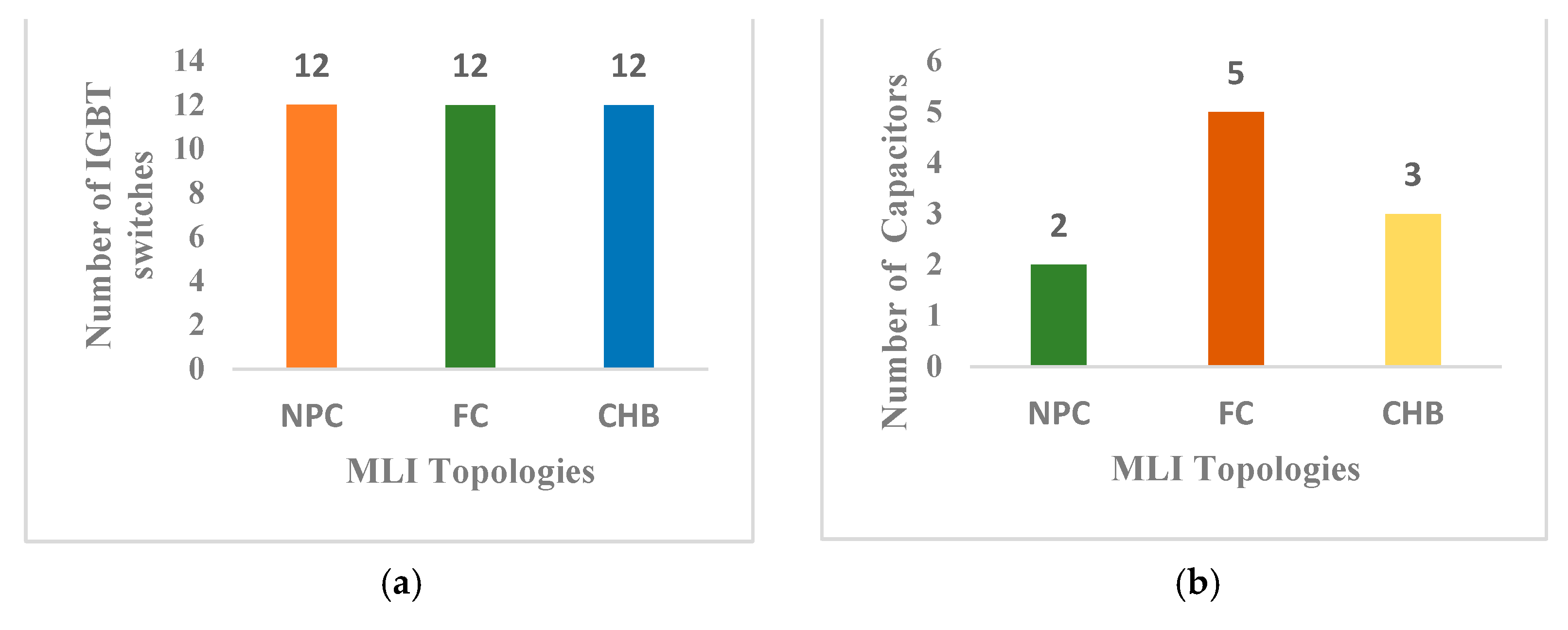
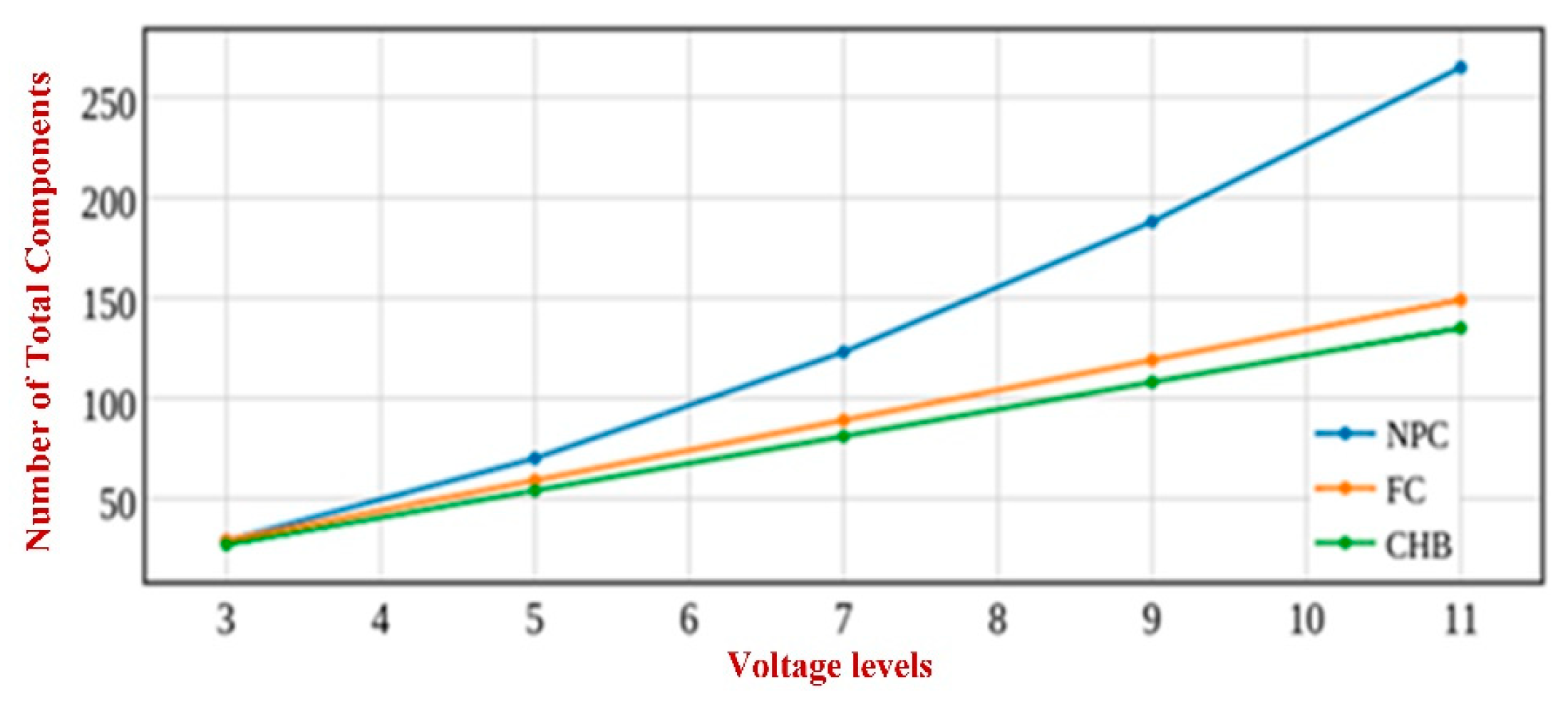
In the investigated inverters, any single component failure in the inverters under study would result in the complete loss of power. An additional factor that might impact a power electronic circuit’s dependability is the total number of components. Figure 20 depicts the correlation between the inverter voltage levels and the total number of circuit components.
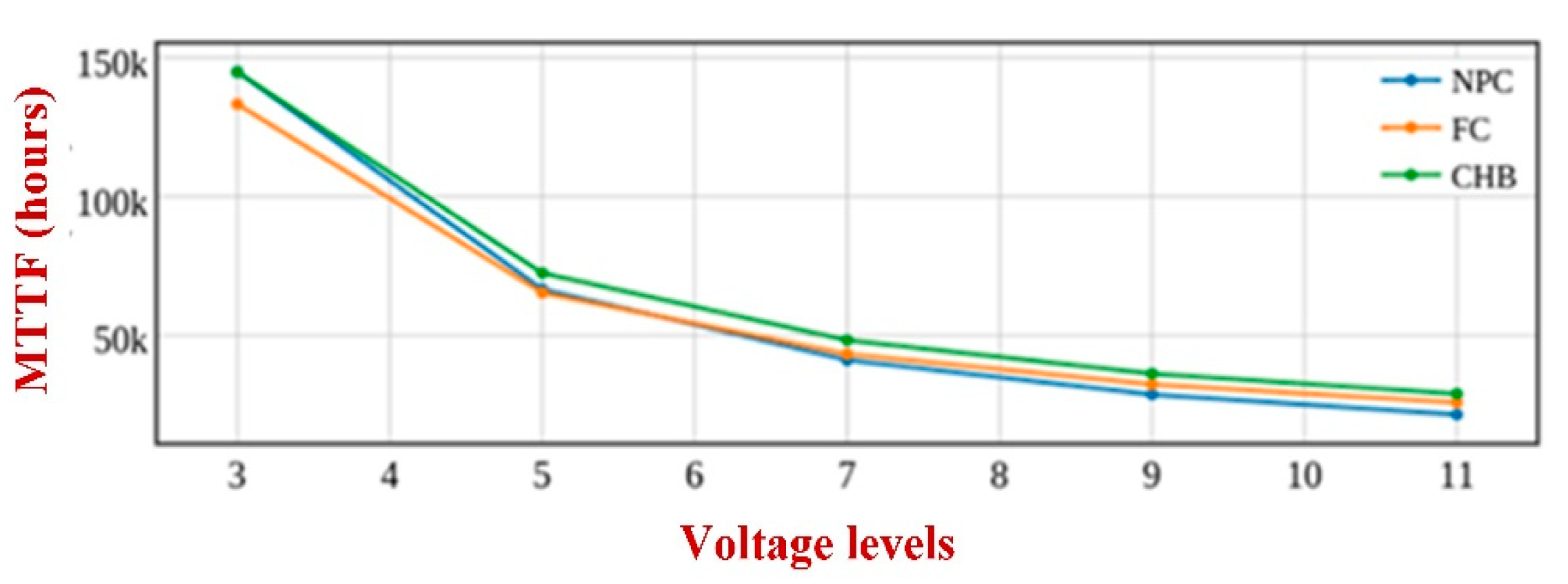
Reliability estimation and the prior quantitative approach reveal that as the number of levels and components increases, then MTTF decreases. Figure 21 shows that it is clear that raising the voltage levels in any one of the three inverters drastically decreases the system’s dependability when a quantitative approach is used. A different approach to calculating the failure rate is thus required to provide a more accurate assessment.
The following Equation (29) from [50] can be used to estimate the overall failure rate of a system.
λ SYS = i = 1 N λ p i
The components stress technique is described. This approach relies heavily on the temperature factor T being accurately calculated. Calculations of power loss in diodes and switches have been made with great precision using the software MATLAB Simulink. The current has been measured with a resistor of 1 ohm. Using Equations (16)–(27), the Pi factors and failure rates for each circuit element are computed for basic three-level three-phase inverters of NPC, FC, and CHB, operating under identical conditions. All three inverters under consideration share the same fundamental specifications, including input voltage (200 V), output frequency (50 Hz), and switching frequency (20 kHz). NPC, FC, and CHB each have their unique maximum output powers, which are 2075, 3750, and 2150 W. Capacitor values employed by the inverters under consideration are also displayed in Table 6, Table 7 and Table 8.
As in Reference [50], we assume a control circuit failure rate of 0.88 over all three inverters. Equation (28) states that the overall failure rate of a system may be computed by multiplying the total number of each component by its failure rate and then adding the resulting products. The conclusive calculations for this analysis are displayed in Table 9.
According to the findings, CHB inverters are more trustworthy. There is a large discrepancy between the estimated method’s calculations and the accurate methods’. Due to the predicted MTTFs being larger than the results of the precise technique, it may be concluded that the approximate method is unsuitable for judging dependability. Both the approximate and accurate techniques are acceptable here since the inverters are equally reliable, regardless of which one is used. There are additional considerations that should be made while choosing an inverter, such as price and performance. Many strategies have been offered to increase the stability of power electronic circuits, but they will not be discussed here. However, the impact of one of the most helpful approaches in this respect should be emphasized.

Series Redundancy

Reliability can be increased by adding components in series in this setup. A single component failure will not bring down the rest of the system. The only restriction on the size of a series is its price. The dependability function [67] for an n-series system is as follows.
R(t) = 1 − (1 − e−λt)n
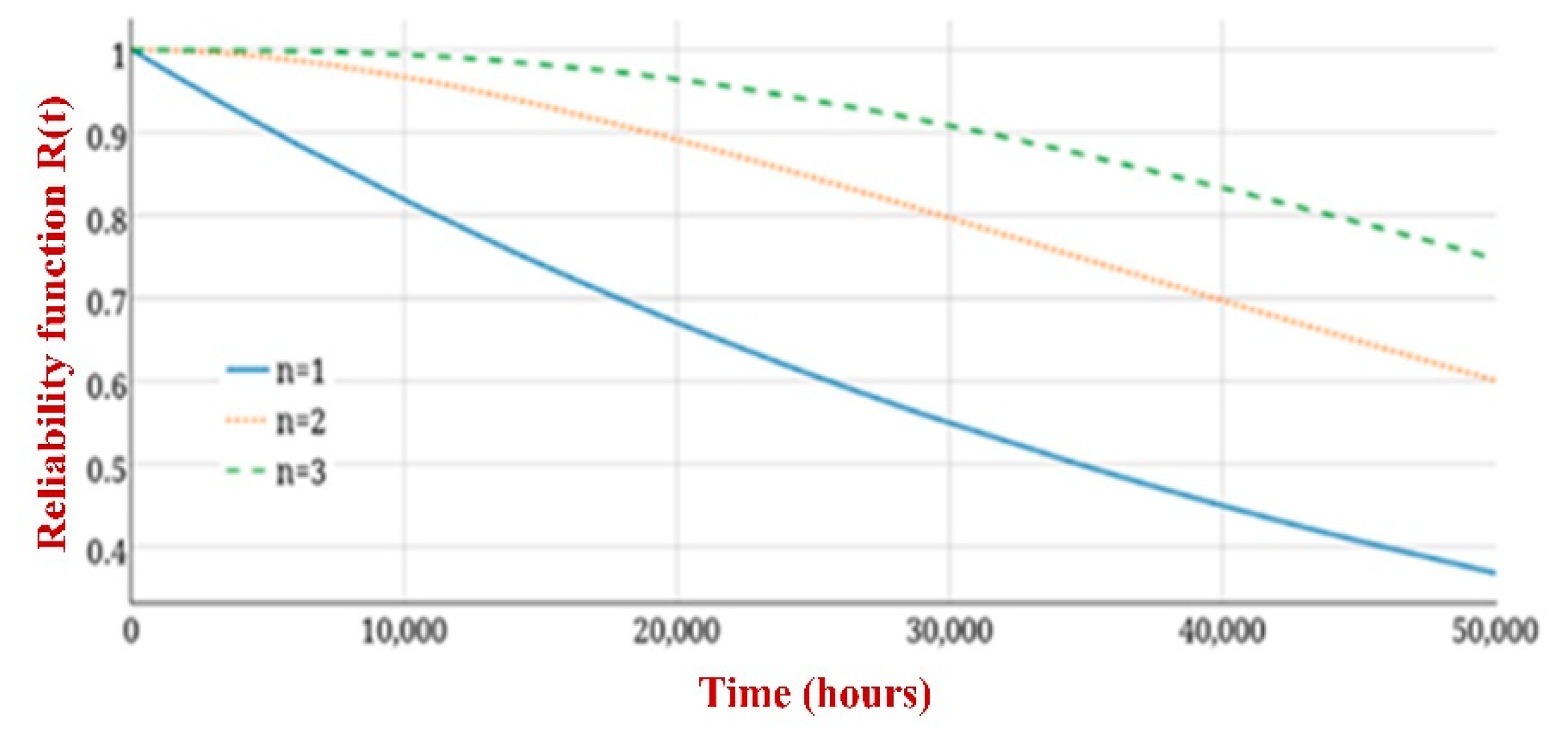
When there are more elements in the series, the dependability function approaches 1, as shown in Equation (30). The results of series redundancy on three multilevel inverters of NPC, FC, and CHB are depicted in Figure 22, Figure 23 and Figure 24.
Power electronics’ reliability has been the subject of several academic investigations. References [67,70] assess the effectiveness of various redundancy architectures and strategies for improving the reliability of power electronic circuits. Redundancy structures in various circuits have received a lot of research and development focus in recent years. Inverters [71,72], matrix converters [73], multilevel converters [74], direct current (DC) to direct current (DC) converters [75], and power factor correction rectifiers [76] all have their own suggested redundancy structures.
To emphasize the significance of the reliability concept in power electronic circuits, this study provides the first-ever assessment of the reliability of three standard multilevel inverters of NPC, FC, and CHB using both approximate and exact methodologies. However, several cutting-edge multilevel inverters, such as Hybrid Multilevel Cells, have not yet had their dependability assessed.
The precise numbers for NPC, FC, and CHB are 50,036, 42,245, and 65,451 h, respectively, as shown in Figure 25, and the findings of the exact technique are comparable to those of the approximation method. By taking into account all of the circumstances for each inverter, the precise technique has the advantage of increasing accuracy. The CHB inverter is the most reliable option, and it may be determined using the suggested methodology. The outcomes demonstrated that the expected failure rates are reliant on the technique employed. In addition, the basic multilevel inverters’ series redundancy idea was explained. The outcomes demonstrated that series redundancy boosts dependability. For NPC, FC, and CHB, the reliability function value improved by approximately 23.26%, 21.24%, and 24.88%, respectively, as shown in Figure 26, with the addition of one redundancy part over 50,000 h.

4. The Effects of PV Array Size on the Durability and Reliability of PV Inverters

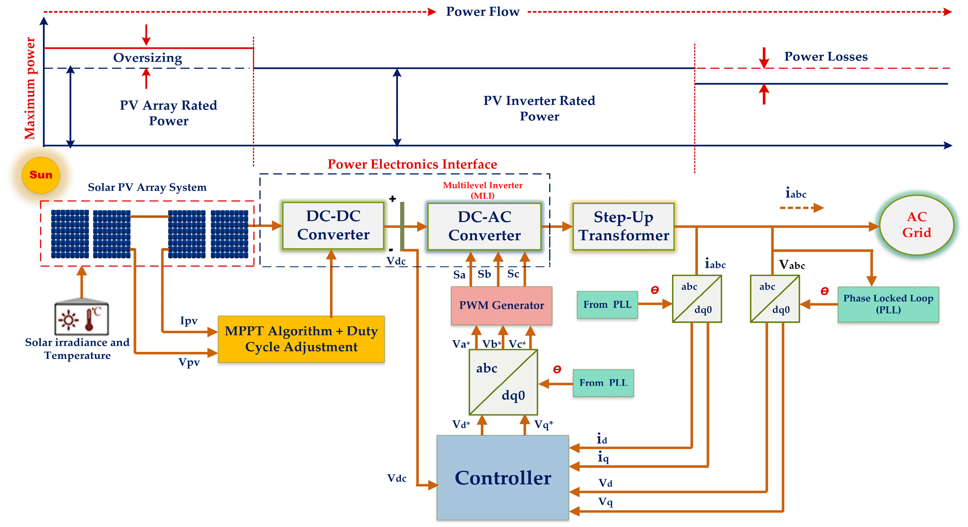
PV power plants may compete with more traditional ones (e.g., fossil-fuel-based systems). According to [77], the price of PV energy (for residential applications in the US) has to drop from its present 0.18 USD/kWh to 0.05 USD/kWh by the year 2030. Reducing the price of PV electricity by more than thrice is an ambitious goal. The aforementioned goal may be reached in many ways, all of which serve to lower the price of PV energy (e.g., improving efficiency and enhancing the component’s lifetime). Oversizing the PV arrays is a typical (and feasible) option, where the rated power of the PV arrays is deliberately built to be higher than the rated power of the PV inverter [78,79,80]. This is seen in Figure 27. More PV energy can be harvested at off-peak times, and the inverter for the panels will be able to function closer to its rated power for a greater fraction of the time. Oversizing PV arrays becomes an appealing alternative with a modest increase in the system cost, and, therefore, a lower overall cost of PV energy [81,82,83], since the price of PV panels continues to fall, with the PV module price falling by roughly 13% per year [84,85,86,87].
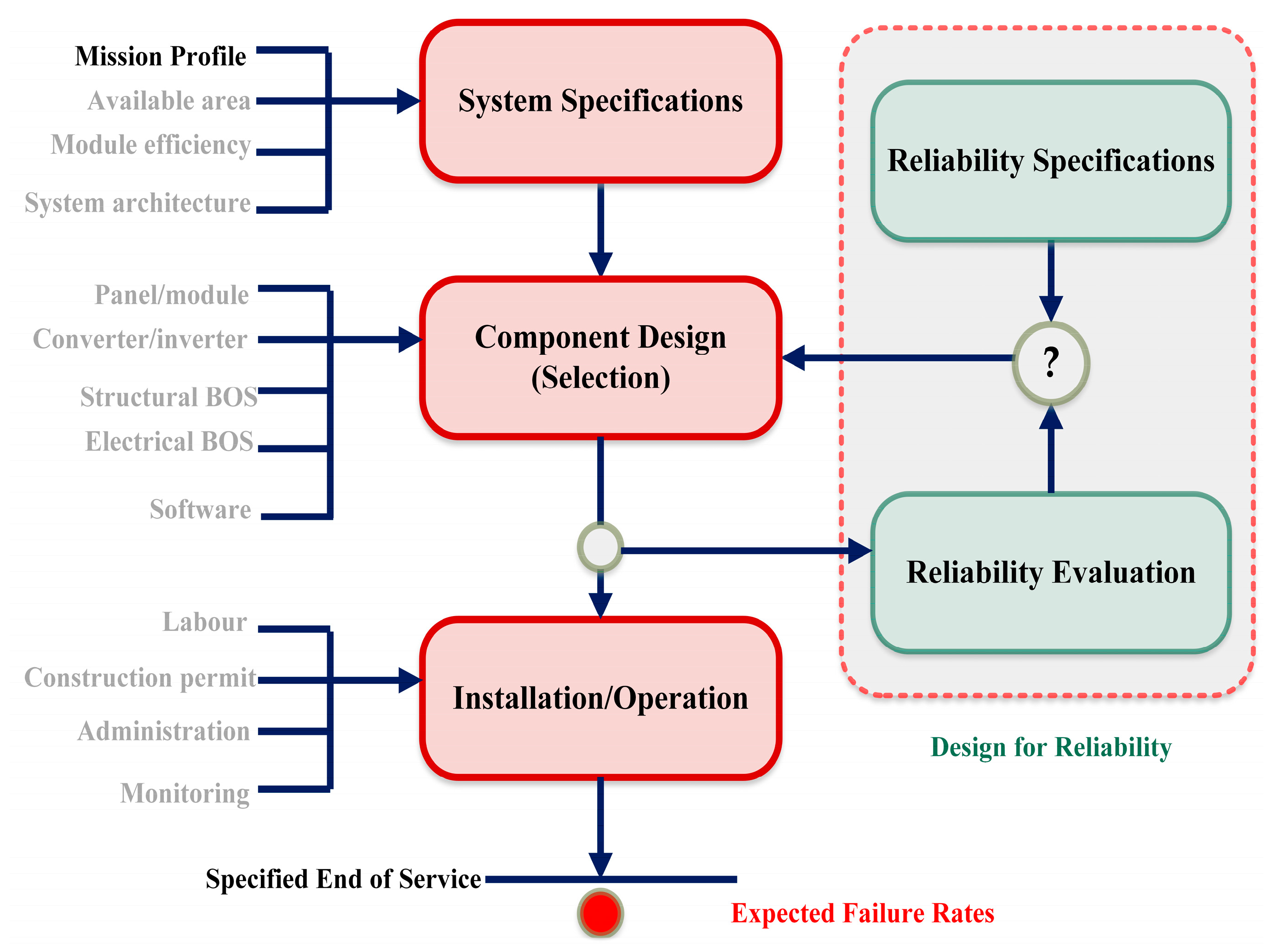
Mission profiles are used to depict how the system is performing in the field [88], as shown in Figure 27. Since PV power generation is very sensitive to both solar irradiation and ambient temperature, these two factors are taken into account while designing a mission profile for PV systems.
Oversizing the PV array, however, will harm the inverter’s loading and dependability. Due to this, the longevity of the system’s components and dependability as a whole may suffer. The PV inverter lifetime is a major factor in the cost evaluation of the PV system [86,87]. Since the cost associated with the PV inverter failure is about 59% of the overall system cost. Costs associated with running and maintaining the PV inverter might become prohibitive, offsetting any savings from the additional energy generated. Both [82] and [85] draw attention to this problem, but they do not provide any extensive lifespan studies. In light of the aforementioned gap and problem, the purpose of this article is to explore the effects of PV array size on the longevity and dependability of PV inverters.
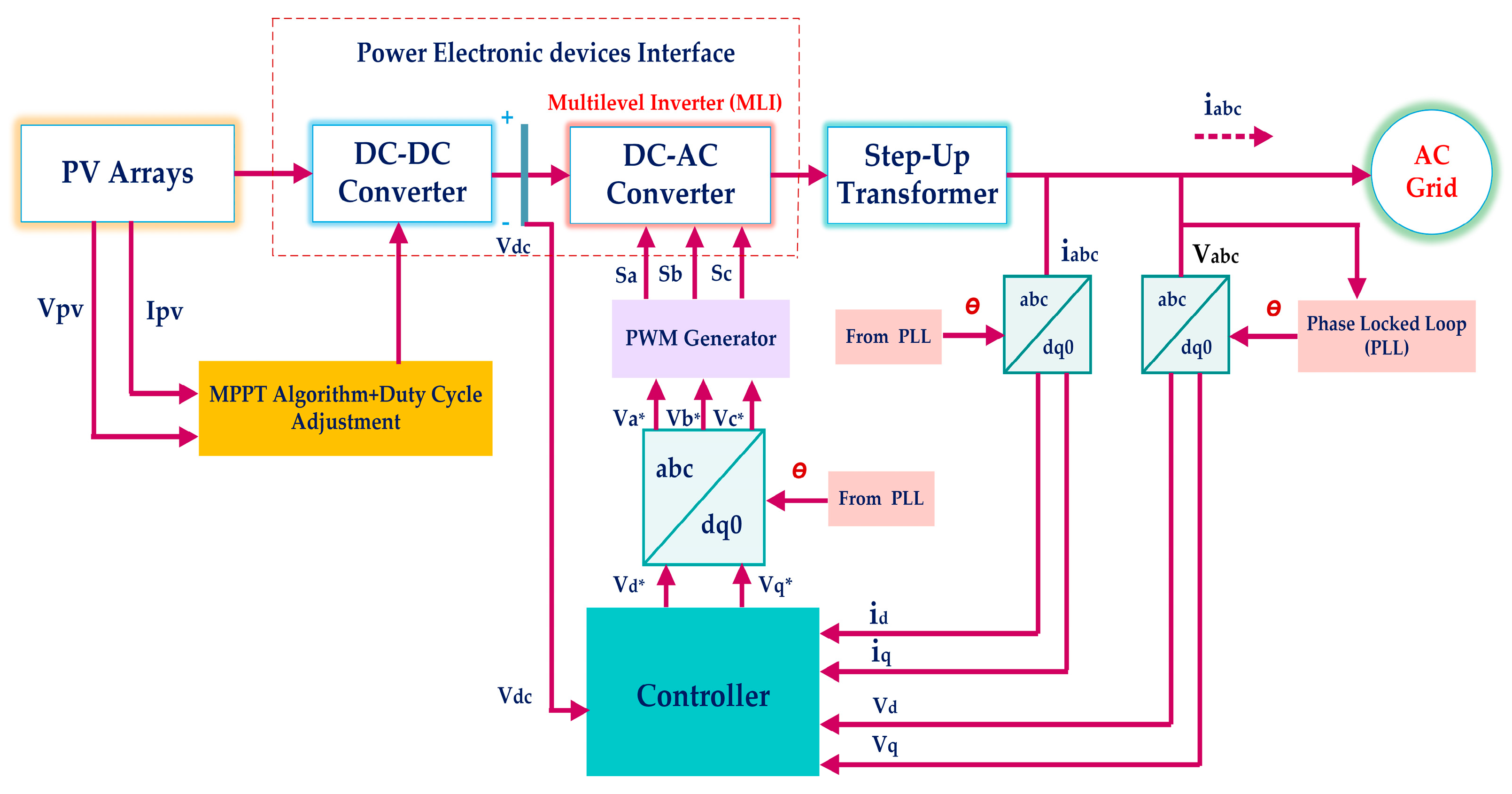
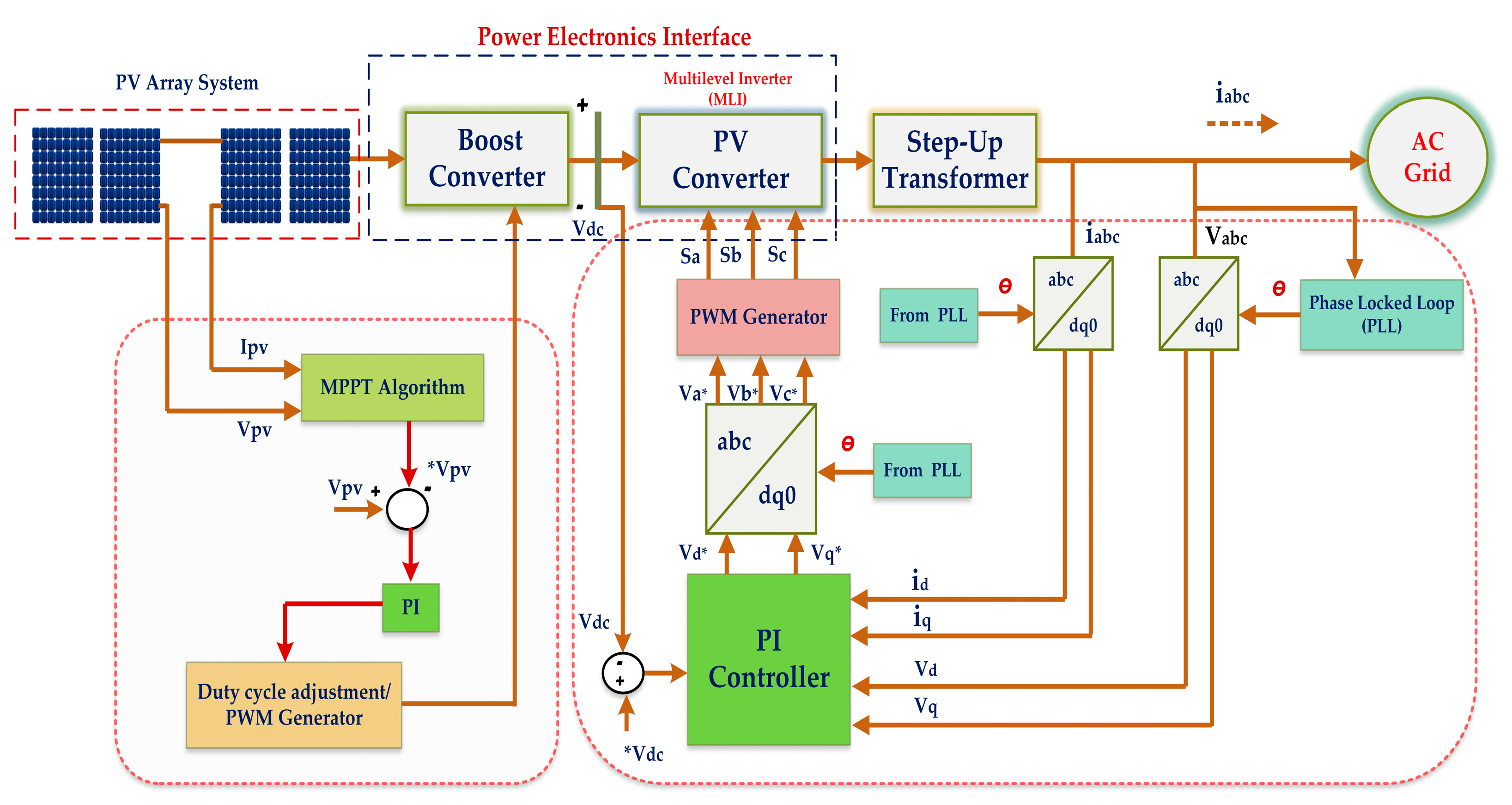
Figure 28 depicts a single-phase grid-connected PV system’s setup and control framework. Two power converters—a boost DC–DC converter and a PV inverter—are used to connect PV arrays with the grid [89]. A boost converter controls the PV power extraction [90]. A Maximum Power Point Tracking (MPPT) method is applied in the boost converter by adjusting the PV voltage Vpv at the PV array’s MPP to maximize solar energy generation. The PV inverter transmits the extracted power to the AC grid by managing the DC-link voltage Vdc using a current controller. PLL is essential for synchronization [91].
The sizing ratio Rs is commonly defined as the ratio of the Standard Test Condition (STC) rated power of the PV array Ppv rated to the rated power of the PV inverter Pinv rated. To maximize PV energy acquisition (even under low solar irradiation), as shown in Figure 29, systems are often built to be large (Rs > 1) in [92,93,94,95]. Installation locations affect the sizing ratio, with the normal value (today) being between 1 and 1.5.
Figure 30 depicts the PV power extraction with bigger PV arrays, where the energy production of the PV system is boosted as a result of the greater energy yield during the Maximum Power Point (MPP) of the sun. Oversized PV arrays in a grid-connected PV system can provide maximum power at all stages of the power conversion process. The situation is a lack of sunlight. However, the performance of the PV inverter, the connection between PV arrays and the grid, might be affected if the PV array is oversized. There is some research on the effects of oversizing the PV array on PV energy costs and methods of design that aim to optimize energy production and its process flow, as shown in Figure 31.

4.1. Mission-Profile-Based Lifetime Estimation

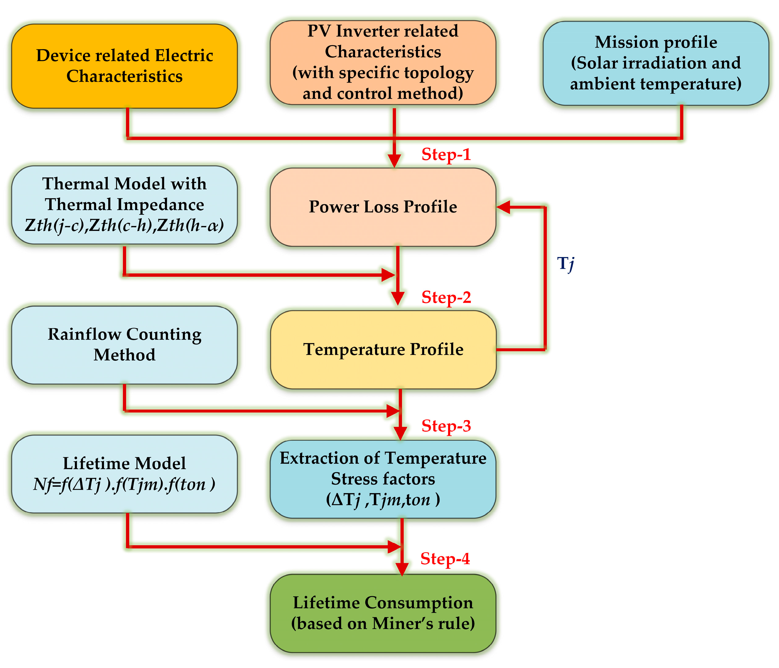
The operational state of the system, known as mission profiles (i.e., solar irradiance and ambient temperature), can have a significant impact on the lifetime of PV inverters [96]. This thermal stress of the PV inverter is directly related to the PV power output, which is, in turn, influenced by the solar irradiation and ambient temperature conditions of the system. Therefore, the mission profile is often included throughout the lifecycle evaluation process, which consists of three primary activities [96,97,98]. First, we need to convert mission profiles into thermal loading conditions; second, we need to understand thermal cycling; and, third, we need to model power devices’ lifetimes. Below, we will fill out the details of the process flow diagram, as shown in Figure 32 and Figure 33.

4.2. Monte Carlo Simulation-Based Lifetime Estimation

Monte Carlo simulations were used in earlier research to evaluate the reliability of power electronics in some different applications. The initial concept was used to forecast the reliability of PV inverters in [99,100], and the others [101,102,103,104] used a similar methodology.
The first step is to do a stress study on the power devices. The study produces a thermal stress profile of the power devices for a specified mission profile, which serves as an input to the whole modeling process. The resultant thermal stress profile is then applied to the lifespan model. Depending on the chosen lifespan model, certain parameters of the thermal cycles must be collected at this stage using a cycle counting technique. These characteristics are then utilized to compute the lifetime consumption of the power devices. In the last stage, Monte Carlo simulations are used to account for fluctuations in the stress and longevity model parameters. The LC for a single year of operation may be estimated using data collected throughout the lifetime assessment. Using a Monte Carlo simulation [101,102,103], we may add uncertainty into the lifespan evaluation process by varying various factors (such as the lifetime model and the stress parameters). Thus, the statistical value of the lifespan distribution and the unreliability function of the power device may be stated, and reliability metrics such as Bx lifetime can be produced [104]. In Figure 34, we see the big picture of the Monte Carlo reliability analysis procedure.

4.2.1. Mission Profile Translation to Thermal Loading

The power devices’ junction temperatures change throughout the operation as a result of stressful circumstances, which are connected to the mission profile of the power devices (e.g., voltages, currents, and environmental temperature). An electro-thermal model of the power converter system is commonly used to obtain this. The input power from the PV panels (PPV) and the environmental temperature together determine the mission profile for the PV inverter (Ta). The junction temperature will fluctuate as a result of the power losses in the power devices and the heatsink. The junction temperature profile (Tj) of the devices may be determined by utilizing the thermal model of the power devices, mentioned in Figure 34, with power losses and the surrounding temperature as input variables.

4.2.2. Thermal Cycle Counting

Power device wear-out failure is mostly caused by thermal cycling, which takes place at the junction temperature of the power device. As a result, the junction temperature profile, which incorporates changes brought on by the ambient temperature and loading circumstances, must be used to derive thermal cycling information. The heat cycles must be identified using a cycle counting technique, such as the Rainflow algorithm, and then grouped according to the cycle period, cycle amplitude, and cycle mean value. The algorithm is utilized to extract the parameters for the chosen lifespan model from the junction temperature profile, including the number of cycles ni, temperature swing Tj, minimum junction temperature Tjm, and heating time ton.

4.2.3. Estimation of the Lifetime Consumption

The empirical lifespan model is used to forecast the number of cycles until failure (Nlf), and it can be calculated from [99] under specific thermal stress conditions. The power cycling test results are often used to determine the lifetime model of the IGBT module and the most common lifetime model for power devices. The Lifetime Consumption (LC) can be calculated from Equation (31), and the power device may be determined after determining the number of cycles to failure using Miner’s rule [99,100].
LC = i n n i N l f
where ni is the number of cycles, and Nlf is the number of cycles to failure for the same cycle and stress condition.
There are different approaches to implementing the Monte Carlo simulation for the reliability assessment, which will affect the results. The three following approaches will be considered: Monte Carlo with static parameters (MC-SP), Monte Carlo with semi-dynamic parameters (MC-SDP), and Monte Carlo with dynamic parameters [99,100].

5. Challenges and Future Work

The improvements in power electronic devices and associated technologies have increased the use of renewable energy systems in the power grid, but there are issues with electricity quality, grid dependability, and security. To assure grid power quality, numerous standards and guidelines have been created for grid-connected RESs. The following areas need additional research based on the examined literature:
  • Challenges:
  • Accelerated aging usually targets one failure mode such as gate oxide deterioration, latch-up, short circuit, bond wire fatigue, etc. In reality, numerous stresses cause device or module breakdowns. Certain mission-profile-based tests cannot replicate operating situations.
  • In many practical applications, all failure prediction factors may not be measurable, limiting aging information.
  • Due to accessibility and environmental considerations, live condition monitoring may not be possible in some applications.
  • Several electrical characteristics, such as RDSON, Vth, etc., differ amongst devices of the same batch due to differences in manufacturing procedures. To create future condition monitoring for each device/module, a baseline must be established before installation.
  • The equipment in real-life operation receives changing loads and different stresses; however, accelerated testing is often done for a constant loading situation.
  • None of the lifespan prediction models are scalable, meaning that simulating the aging of a lower-rated device would not shed light on the aging of a similar, higher-rated device. In particular, for broad bandgap devices, the magnitude of the parasitic parameters does not rise linearly with the higher rating of the device, and it varies considerably, even among the same rated devices.
  • To fulfill the high grid code requirements and handle the power quality concerns cost-effectively, researchers have, lately, started to design hybrid topologies. It is necessary to explore the performance of these innovative topologies in grid-integrated applications, since most of them have not been assessed in grid-connected RESs.
  • For the grid-connected RES applications, further research is required into the performance analysis of contemporary MLIs. Smart grid solutions need to take MLIs into account as well.
  • Opportunities:
  • Now, there is a window of opportunity to investigate the reliability concerns of emerging technologies that make use of wide bandgap semiconductors.
  • We will be able to access the modules in any practical application if we develop a universal strategy, such as integrating a reflectometry method at the gate drives and gathering all required data.
  • The rating of the prognostic hardware will be greatly reduced by moving to the gate terminal in addition to providing access to every power electronic device at the lower potential terminals.
  • To prevent measuring any electrical parameters and ensure there is no human mistake, Spread-spectrum time-domain reflectometry (SSTDR)-based live condition monitoring might be recommended.

6. Conclusions

This review paper has quickly summarized multilevel inverters to emphasize the necessity for grid-connected PV systems. This review paper presented an overview of the grid-connected multilevel inverters for PV systems with motivational factors, features, assessment parameters, topologies, modulation schemes of the multilevel inverter, performance parameters, and the selection process for specific applications. In this review paper, the findings of a comprehensive reliability analysis of fundamental multilevel inverters are studied and the reliability of three basic multilevel inverters was evaluated. Two distinct methodologies for reliability testing multilevel inverters were presented in this review paper (exact and approximate). The lifespans of NPC, FC, and CHB were 50,036, 42,245, and 65,451 h, respectively, as the findings of the exact technique were comparable to those of the approximation method. By taking into account all of the circumstances for each inverter, the exact technique had the advantage of increasing accuracy, and the CHB inverter was the most reliable option. In addition, the basic multilevel inverters’ series redundancy idea was explained. The outcomes demonstrated that series redundancy boosted reliability and for NPC, FC, and CHB, and the reliability function value improved by approximately 23.26%, 21.24%, and 24.88%, respectively, with the addition of one redundancy part over 50,000 h. In addition, the concept of oversizing photovoltaic (PV) arrays was studied. Finally, the mission-profile-based and Monte Carlo simulation-based methods process flows are discussed for the accurate lifetime prediction and reliability assessment of a PV inverter in a real-time scenario.

Author Contributions

Conceptualization and methodology, S.N.; validation, S.N., D.C., and S.M.M.; formal analysis, S.N.; investigation, D.C.; resources, D.C.; data curation, S.N.; writing—original draft preparation, S.N.; writing—review and editing, D.C.; visualization, D.C.; supervision, D.C. and S.M.M.; project administration, D.C. and S.M.M.; funding acquisition, S.M.M. All authors have read and agreed to the published version of the manuscript.

Funding

This research received no external funding.

Data Availability Statement

This review has no information related to it.

Acknowledgments

The authors, likewise, wish to thank the particular copyright holders for allowing approval to use the pictures, graphics, tables, and figures in this work.

Conflicts of Interest

The authors declare no conflict of interest.

Abbreviations

MLIsMultilevel Inverters
CHB-MLICascaded H-Bridge Multilevel Inverter
TSVTotal Standing Voltage
PVPhotovoltaic
MPPTMaximum Power Point Tracking
THDTotal Harmonic Distortion
EMIElectro-Magnetic Interference
MMCModular Multilevel Converter
FC-MLIFlying Capacitor Multilevel Inverter
SOCState of Charge
NPCNeutral Point Clamped
BESSBattery Energy Storage System
PWMPulse Width Modulation
FRFailure rate
MTTFMean time to failure
MTTRMean time to repair
MTBFMean time between failures
PIProportional plus Integral controller
SHESelective harmonic elimination
NVCNearest vector control
PWMPulse width modulation
SVPWMSpace vector pulse width modulation
RSC-MLIReduced switch count multilevel inverter
TDDBTime-dependent dielectric breakdown
MOSFETMetal–oxide–semiconductor field-effect transistor
IGBTInsulated Gate Bipolar Transistor

Nomenclature

λpExpected failure rate
λOFailure rate due to operational stresses
λeFailure rate due to environmental stresses
λCFailure rate due to temperature cycling stresses
λSjFailure rate due to solder joints
λiFailure rate due to induced stresses
AScaling factor for the rate of failure
TTemperature,
ΔTChange in temperatures
SStress ratio
λbSwitch and diode base failure rates
THSInductor’s hot spot (heat sink) temperature
TAAmbient temperature
πTTemperature factor of switch and diode
TCHeat sink temperature
θjcThermal resistance of the diode or switch
PlossPower loss of the diode or switch:
VSRatio of operating voltage to rated voltage.
πCVFailure rate of capacitors
πQQuality factor
πEEnvironmental factor
πAApplication factor
πCContact construction factor

References

  1. Hasan, K.; Yousuf, S.B.; Tushar, M.S.H.K.; Das, B.K.; Das, P.; Islam, S. Effects of different environmental and operational factors on the PV performance: A comprehensive review. Energy Sci. Eng. 2021, 10, 656–675. [Google Scholar] [CrossRef]
  2. Alavi, O.; Viki, A.H.; Shamlou, S. A Comparative Reliability Study of Three Fundamental Multilevel Inverters Using Two Different Approaches. Electronics 2016, 5, 18. [Google Scholar] [CrossRef]
  3. Dhanamjayulu, C.; Prasad, D.; Padmanaban, S.; Maroti, P.K.; Holm-Nielsen, J.B.; Blaabjerg, F. Design and Implementation of Seventeen Level Inverter With Reduced Components. IEEE Access 2021, 9, 16746–16760. [Google Scholar] [CrossRef]
  4. Dhanamjayulu, C.; Padmanaban, S.; Holm-Nielsen, J.B.; Blaabjerg, F. Design and Implementation of a Single-Phase 15-Level Inverter With Reduced Components for Solar PV Applications. IEEE Access 2020, 9, 581–594. [Google Scholar] [CrossRef]
  5. Khasim, S.R.; Dhanamjayulu, C.; Padmanaban, S.; Holm-Nielsen, J.B.; Mitolo, M. A Novel Asymmetrical 21-Level Inverter for Solar PV Energy System With Reduced Switch Count. IEEE Access 2021, 9, 11761–11775. [Google Scholar] [CrossRef]
  6. Dhanamjayulu, C.; Rudravaram, V.; Sanjeevikumar, P. Design and implementation of a novel 35-level inverter topology with reduced switch count. Electr. Power Syst. Res. 2022, 212, 108641. [Google Scholar] [CrossRef]
  7. Khasim, S.R.; Dhanamjayulu, C. Design and Implementation of Asymmetrical Multilevel Inverter With Reduced Components and Low Voltage Stress. IEEE Access 2022, 10, 3495–3511. [Google Scholar] [CrossRef]
  8. Rodriguez, J.; Lai, J.-S.; Peng, F.Z. Multilevel inverters: A survey of topologies, controls, and applications. IEEE Trans. Ind. Electron. 2002, 49, 724–738. [Google Scholar] [CrossRef]
  9. Dhanamjayulu, C.; Padmanaban, S. A Novel Neutral Point Clamped Symmetrical Boost Inverters with Reduced Components. In Proceedings of the 2021 IEEE 12th Energy Conversion Congress & Exposition-Asia (ECCE-Asia), Singapore, 24–27 May 2021; pp. 1431–1436. [Google Scholar] [CrossRef]
  10. Prasad, D.; Dhanamjayulu, C.; Padmanaban, S.; Holm-Nielsen, J.B.; Blaabjerg, F.; Khasim, S.R. Design and Implementation of 31-Level Asymmetrical Inverter with Reduced Components. IEEE Access 2021, 9, 22788–22803. [Google Scholar] [CrossRef]
  11. Rodriguez, J.; Bernet, S.; Wu, B.; Pontt, J.O.; Kouro, S. Multilevel Voltage-Source-Converter Topologies for Industrial Medium-Voltage Drives. IEEE Trans. Ind. Electron. 2007, 54, 2930–2945. [Google Scholar] [CrossRef]
  12. Rodriguez, J.; Bernet, S.; Steimer, P.K.; Lizama, I.E. A Survey on Neutral-Point-Clamped Inverters. IEEE Trans. Ind. Electron. 2010, 57, 2219–2230. [Google Scholar] [CrossRef]
  13. Kouro, S.; Leon, J.I.; Vinnikov, D.; Franquelo, L.G. Grid-Connected Photovoltaic Systems: An Overview of Recent Research and Emerging PV Converter Technology. IEEE Ind. Electron. Mag. 2015, 9, 47–61. [Google Scholar] [CrossRef]
  14. Hassaine, L.; Olias, E.; Quintero, J.; Salas, V. Overview of power inverter topologies and control structures for grid connected photovoltaic systems. Renew. Sustain. Energy Rev. 2014, 30, 796–807. [Google Scholar] [CrossRef]
  15. Daher, S.; Schmid, J.; Antunes, F.L.M. Multilevel Inverter Topologies for Stand-Alone PV Systems. IEEE Trans. Ind. Electron. 2008, 55, 2703–2712. [Google Scholar] [CrossRef]
  16. Murugesan, M.; Pari, R.; Sivakumar, R.; Sivaranjani, S. Different types of multilevel inverter topologies—A technical Review. Int. J. Adv. Engg. Tech. 2016, 7, 155. [Google Scholar]
  17. Hasan, N.S.; Rosmin, N.; Osman, D.A.A.; Musta’amal@Jamal, A.H. Reviews on multilevel converter and modulation techniques. Renew. Sustain. Energy Rev. 2017, 80, 163–174. [Google Scholar] [CrossRef]
  18. Kala, P.; Arora, S. A comprehensive study of classical and hybrid multilevel inverter topologies for renewable energy applications. Renew. Sustain. Energy Rev. 2017, 76, 905–931. [Google Scholar] [CrossRef]
  19. Shehu, G.S.; Kunya, A.B.; Shanono, I.H.; Yalcinoz, T. A Review of Multilevel Inverter Topology and Control Techniques. J. Autom. Control. Eng. 2016, 4, 233–241. [Google Scholar] [CrossRef]
  20. Nyamathulla, S.; Dhanamjayulu, C. Design of 17-Level Inverter with Reduced Switch Count. In Proceedings of the 2021 Innovations in Power and Advanced Computing Technologies (i-PACT), Kuala Lumpur, Malaysia, 27–29 November 2021; pp. 1–8. [Google Scholar]
  21. Chattopadhyay, S.K.; Chakraborty, C. Three-Phase Hybrid Cascaded Multilevel Inverter Using Topological Modules With 1:7 Ratio of Asymmetry. IEEE J. Emerg. Sel. Top. Power Electron. 2018, 6, 2302–2314. [Google Scholar] [CrossRef]
  22. Callegari, J.; Silva, M.; de Barros, R.; Brito, E.; Cupertino, A.; Pereira, H. Lifetime evaluation of three-phase multifunctional PV inverters with reactive power compensation. Electr. Power Syst. Res. 2019, 175, 105873. [Google Scholar] [CrossRef]
  23. Hanif, A.; Yu, Y.; DeVoto, D.; Khan, F.H. A Comprehensive Review Toward the State-of-the-Art in Failure and Lifetime Predictions of Power Electronic Devices. IEEE Trans. Power Electron. 2018, 34, 4729–4746. [Google Scholar] [CrossRef]
  24. Yang, S.; Xiang, D.; Bryant, A.; Mawby, P.; Ran, L.; Tavner, P. Condition Monitoring for Device Reliability in Power Electronic Converters: A Review. IEEE Trans. Power Electron. 2010, 25, 2734–2752. [Google Scholar] [CrossRef]
  25. Wang, C.; Ji, B.; Song, X.; Pickert, V.; Cao, W. IGBT condition monitoring with system identification methods. In Proceedings of the 2014 IEEE Conference and Expo Transportation Electrification Asia-Pacific (ITEC Asia-Pacific), Beijing, China, 31 August–3 September 2014. [Google Scholar] [CrossRef]
  26. Physical Characterization Group. Selected failure mechanisms of modern power modules. Microelectron. Reliab. 2002, 42, 653–667. [Google Scholar] [CrossRef]
  27. Krebs, T.; Duch, S.; Schmitt, W.; Kotter, S.; Prenosil, P.; Thomas, S. A breakthrough in power electronics reliability New die attach and wire bonding materials. In Proceedings of the 2013 IEEE 63rd Electronic Components and Technology Conference, Las Vegas, NV, USA, 28–31 May 2013; pp. 1746–1752. [Google Scholar] [CrossRef]
  28. Hinata, Y.; Horio, M.; Ikeda, Y.; Yamada, R.; Takahashi, Y. Full SiC power module with advanced structure and its solar inverter application. In Proceedings of the 2013 Twenty-Eighth Annual IEEE Applied Power Electronics Conference and Exposition (APEC), Long Beach, CA, USA, 17–21 March 2013; pp. 604–607. [Google Scholar] [CrossRef]
  29. Nguyen, T.-T.; Ahmed, A.; Thang, T.V.; Park, J.-H. Gate Oxide Reliability Issues of SiC MOSFETs Under Short-Circuit Operation. IEEE Trans. Power Electron. 2014, 30, 2445–2455. [Google Scholar] [CrossRef]
  30. Vaalasranta, I.; Pippola, J.; Frisk, L. Power MOSFET failure and degradation mechanisms in fly back topology under high temperature and high humidity conditions. In Proceedings of the 9th 2013 9th IEEE International Symposium on Diagnostics for Electric Machines, Power Electronics and Drives (SDEMPED), Valencia, Spain, 27–30 August 2013; pp. 16–22. [Google Scholar]
  31. Lombardo, S.; Stathis, J.H.; Linder, B.P.; Pey, K.L.; Palumbo, F.; Tung, C.H. Dielectric breakdown mechanisms in gate oxides. J. Appl. Phys. 2005, 98, 121301. [Google Scholar] [CrossRef]
  32. Sonnenfeld, G.; Goebel, K.; Celaya, J.R. An agile accelerated aging, characterization and scenario simulation system for gate controlled power transistors. In Proceedings of the 2008 IEEE AUTOTESTCON, Salt Lake City, UT, USA, 8–11 September 2008; pp. 208–215. [Google Scholar] [CrossRef]
  33. Benbahouche, L.; Merabet, A.; Zegadi, A. A comprehensive analysis of failure mechanisms: Latch up and second breakdown in IGBT(IXYS) and improvement. In Proceedings of the 2012 19th International Conference on Microwaves, Radar & Wireless Communications, Warsaw, Poland, 21–23 May 2012; Volume 1, pp. 190–192. [Google Scholar] [CrossRef]
  34. Patil, N.; Celaya, J.; Das, D.; Goebel, K.; Pecht, M. Precursor Parameter Identification for Insulated Gate Bipolar Transistor (IGBT) Prognostics. IEEE Trans. Reliab. 2009, 58, 271–276. [Google Scholar] [CrossRef]
  35. Bouarroudj, M.; Khatir, Z.; Ousten, J.-P.; Lefebvre, S. Temperature-Level Effect on Solder Lifetime During Thermal Cycling of Power Modules. IEEE Trans. Device Mater. Reliab. 2008, 8, 471–477. [Google Scholar] [CrossRef]
  36. Patil, N.; Das, D.; Pecht, M. A prognostic approach for non-punch through and field stop IGBTs. Microelectron. Reliab. 2011, 52, 482–488. [Google Scholar] [CrossRef]
  37. Pietranico, S.; Lefebvre, S.; Pommier, S.; Bouaroudj, M.B.; Bontemps, S. A study of the effect of degradation of the aluminum metallization layer in the case of power semiconductor devices. Microelectron. Reliab. 2011, 51, 1824–1829. [Google Scholar] [CrossRef]
  38. Valentine, N.; Das, D.; Pecht, M. Failure mechanisms of insulated gate bipolar transistors (IGBTs). In Proceedings of the NREL Photovoltaic Reliability Workshop 2015, Golden, CO, USA, 24–27 February 2015; pp. 6–10. [Google Scholar]
  39. Lee, Y.; Hwang, D. A study on the techniques of estimating the probability of failure. J. Chungcheong Math. Soc. 2008, 21, 573–583. [Google Scholar]
  40. Song, Y.; Wang, B. Survey on Reliability of Power Electronic Systems. IEEE Trans. Power Electron. 2012, 28, 591–604. [Google Scholar] [CrossRef]
  41. Wang, H.; Ma, K.; Blaabjerg, F. Design for reliability of power electronic systems. In Proceedings of the 38th Annual Conference on IEEE Industrial Electronics Society, Montreal, QC, Canada, 25–28 October 2012; pp. 33–44. [Google Scholar]
  42. Dhanamjayulu, C.; Sanjeevikumar, P.; Muyeen, S.M. A structural overview on transformer and transformer-less multilevel inverters for renewable energy applications. Energy Rep. 2022, 8, 10299–10333. [Google Scholar]
  43. Klutke, G.; Kiessler, P.; Wortman, M. A critical look at the bathtub curve. IEEE Trans. Reliab. 2003, 52, 125–129. [Google Scholar] [CrossRef]
  44. Birolini, A. Reliability Engineering, 5th ed.; Springer: Berlin/Heidelberg, Germany, 2007. [Google Scholar]
  45. Lyu, M.R. Handbook of Software Reliability Engineering; IEEE Computer Society Press & McGraw-Hill: Hightstown, NJ, USA, 1996. [Google Scholar]
  46. Stapelberg, R.F. Handbook of Reliability, Availability, Maintainability and Safety in Engineering Design; Springer Science & Business Media: Berlin/Heidelberg, Germany, 2009. [Google Scholar]
  47. Rausand, M.; Hoyland, A. System Reliability Theory: Models, Statistical Methods, and Applications; John Wiley & Sons: Hoboken, NJ, USA, 2004. [Google Scholar]
  48. Yang, N.; Dhillon, B. Availability analysis of a repairable standby human-machine system. Microelectron. Reliab. 1995, 35, 1401–1413. [Google Scholar] [CrossRef]
  49. Goel, A. A New Approach to Electronic Systems Reliability Assessment. Ph.D. Thesis, Rensselaer Polytechnic Institute, Troy, NY, USA, 2007. [Google Scholar]
  50. Abdi, B.; Ranjbar, A.H.; Gharehpetian, G.B.; Milimonfared, J. Reliability Considerations for Parallel Performance of Semiconductor Switches in High-Power Switching Power Supplies. IEEE Trans. Ind. Electron. 2009, 56, 2133–2139. [Google Scholar] [CrossRef]
  51. Ranjbar, A.H.; Abdi, B.; Gharehpetian, G.B.; Fahimi, B. Reliability assessment of single-stage/two-stage PFC converters. In Proceedings of the 2009 Compatibility and Power Electronics, Badajoz, Spain, 20–22 May 2009; pp. 253–257. [Google Scholar] [CrossRef]
  52. SAE G-11 Committee. Aerospace Information Report on Reliability Prediction Methodologies for Electronic Equipment AIR5286; Draft Report; SAE: Warrendale, PA, USA, 1998. [Google Scholar]
  53. Siemens, A.G. Siemens Company Standard SN29500 (Version 6.0). Failure Rates of Electronic Components. Siemens Technical Liaison and Standardization; Siemens AG: Munich, Germany, 1999. [Google Scholar]
  54. Union Technique de L’Electricité. RDF 2000: Reliability Data Handbook; Union Technique de L’Electricité: Nanterre, France, 2000. [Google Scholar]
  55. Kiran, S.R.; Basha, C.H.H.; Singh, V.P.; Dhanamjayulu, C.; Prusty, B.R.; Khan, B. Reduced Simulative Performance Analysis of Variable Step Size ANN Based MPPT Techniques for Partially Shaded Solar PV Systems. IEEE Access 2022, 10, 48875–48889. [Google Scholar] [CrossRef]
  56. Telcordia Technologies. Special Report SR-332: Reliability Prediction Procedure for Electronic Equipment (Issue 1); Telcordia Customer Service; Telcordia Technologies AG: Piscataway, NJ, USA, 2001. [Google Scholar]
  57. British Telecom. Handbook of Reliability Data for Components Used in Telecommunication Systems; British Telecom: Birmingham, UK, 1987. [Google Scholar]
  58. Pecht, M.; Nash, F. Predicting the reliability of electronic equipment. Proc. IEEE 1994, 82, 992–1004. [Google Scholar] [CrossRef]
  59. Empowering the Reliability Professional. Available online: http://www.reliasoft.com/ (accessed on 18 December 2011).
  60. Jones, A.; Hayes, J. A comparison of electronic reliability prediction methodologies. IEEE Trans. Reliab. 1999, 48, 127–134. [Google Scholar] [CrossRef]
  61. EATON White Paper TD02000001E. The Reliability of Neutral Point Clamped vs. Cascaded H-Bridge Inverters. October 2009. Available online: http://www.eaton.com (accessed on 15 April 2016).
  62. Krug, D.; Bernet, S.; Fazel, S.S.; Jalili, K.; Malinowski, M. Comparison of 2.3-kV Medium-Voltage Multilevel Converters for Industrial Medium-Voltage Drives. IEEE Trans. Ind. Electron. 2007, 54, 2979–2992. [Google Scholar] [CrossRef]
  63. Anderson, R.T. Reliability Design Handbook; ITT Research Institute: Chicago, IL, USA, 1976. [Google Scholar]
  64. Dylis, D.D.; Priore, M.G. A comprehensive reliability assessment tool for electronic systems. In Proceedings of the IEEE Annual Reliability and Maintainability Symposium, Philadelphia, PA, USA, 22–25 January 2001; pp. 308–313. [Google Scholar]
  65. Lu, H.; Bailey, C.; Yin, C. Design for reliability of power electronics modules. Microelectron. Reliab. 2009, 49, 1250–1255. [Google Scholar] [CrossRef]
  66. Khosroshahi, A.; Abapour, M.; Sabahi, M. Reliability Evaluation of Conventional and Interleaved DC–DC Boost Converters. IEEE Trans. Power Electron. 2014, 30, 5821–5828. [Google Scholar] [CrossRef]
  67. Richardeau, F.; Pham, T.T.L. Reliability Calculation of Multilevel Converters: Theory and Applications. IEEE Trans. Ind. Electron. 2012, 60, 4225–4233. [Google Scholar] [CrossRef]
  68. US Department of Defense. MIL-HDBK-217F (NOTICE 2), Military Handbook Reliability Prediction of Electronic Equipment; Defense Technical Information Center: Alexandria, VA, USA, 1995.
  69. Graovac, D.; Pürschel, M. IGBT Power Losses Calculation Using the Data-Sheet Parameters; Infineon Application Note; Infineon Technologies AG: Neubiberg, Germany, 2009; pp. 1–17. [Google Scholar]
  70. Chiodo, E.; Lauria, D. Some Basic Properties of the Failure Rate of Redundant Reliability Systems in Industrial Electronics Applications. IEEE Trans. Ind. Electron. 2015, 62, 5055–5062. [Google Scholar] [CrossRef]
  71. Li, S.; Xu, L. Strategies of fault tolerant operation for three-level PWM inverters. IEEE Trans. Power Electron. 2006, 21, 933–940. [Google Scholar] [CrossRef]
  72. Ceballos, S.; Pou, J.; Zaragoza, J.; Martin, J.L.; Robles, E.; Gabiola, I.; Ibanez, P. Efficient Modulation Technique for a Four-Leg Fault-Tolerant Neutral-Point-Clamped Inverter. IEEE Trans. Ind. Electron. 2008, 55, 1067–1074. [Google Scholar] [CrossRef]
  73. Nguyen-Duy, K.; Liu, T.-H.; Chen, D.-F.; Hung, J.Y. Improvement of Matrix Converter Drive Reliability by Online Fault Detection and a Fault-Tolerant Switching Strategy. IEEE Trans. Ind. Electron. 2011, 59, 244–256. [Google Scholar] [CrossRef]
  74. Barriuso, P.; Dixon, J.; Flores, P.; Moran, L. Fault-Tolerant Reconfiguration System for Asymmetric Multilevel Converters Using Bidirectional Power Switches. IEEE Trans. Ind. Electron. 2008, 56, 1300–1306. [Google Scholar] [CrossRef]
  75. Ambusaidi, K.; Pickert, V.; Zahawi, B. New Circuit Topology for Fault Tolerant H-Bridge DC–DC Converter. IEEE Trans. Power Electron. 2009, 25, 1509–1516. [Google Scholar] [CrossRef]
  76. Pham, T.T.L.; Richardeau, F.; Gateau, G. Diagnosis strategies and reconfiguration of a 5-level double-boost PFC with fault-tolerant capability. In Proceedings of the 2011 IEEE International Symposium on Industrial Electronics, Gdansk, Poland, 27–30 June 2011; pp. 1857–1862. [Google Scholar] [CrossRef]
  77. Sangwongwanich, A.; Yang, Y.; Sera, D.; Blaabjerg, F. Impacts of PV array sizing on PV inverter lifetime and reliability. In Proceedings of the 2017 IEEE Energy Conversion Congress and Exposition (ECCE), Cincinnati, OH, USA, 1–5 October 2017; pp. 3830–3837. [Google Scholar] [CrossRef]
  78. Fiorelli, J.; Zuercher-Martinson, M. How oversizing your array to-inverter ratio can improve solar-power system performance. Solar Power World 2013, 7, 42–48. [Google Scholar]
  79. Khatib, T.; Mohamed, A.; Sopian, K. A review of photovoltaic systems size optimization techniques. Renew. Sustain. Energy Rev. 2013, 22, 454–465. [Google Scholar] [CrossRef]
  80. Prasad, D.; Dhanamjayulu, C. Reduced Voltage Stress Asymmetrical Multilevel Inverter With Optimal Components. IEEE Access 2022, 10, 53546–53559. [Google Scholar] [CrossRef]
  81. SMA. 7 Reasons Why You Should Oversize Your PV Array. December 2015. Available online: https://www.sma-sunny.com/en/7-reasons-why-you-should-oversize-your-pv-array-2/ (accessed on 1 January 2022).
  82. Global Sustainable Energy Solutions (GSES) India. Oversizing PV Arrays; Technical Report; 2014; Available online: https://gses.in/old-gses-in/publications/resources-and-information/oversizing-pv-arrays (accessed on 1 January 2022).
  83. Solar Edge. Oversizing of Solar Edge Inverters, Technical Note; Technical Report; July 2016; Available online: https://knowledge-center.solaredge.com/sites/kc/files/inverter_dc_oversizing_guide.pdf (accessed on 1 January 2022).
  84. Prasad, D.; Dhanamjayulu, C. Solar PV-Fed Multilevel Inverter with Series Compensator for Power Quality Improvement in Grid-Connected Systems. IEEE Access 2022, 10, 81203–81219. [Google Scholar] [CrossRef]
  85. Good, J.; Johnson, J. Impact of inverter loading ratio on solar photovoltaic system performance. Appl. Energy 2016, 177, 475–486. [Google Scholar] [CrossRef]
  86. Moore, L.M.; Post, H.N. Five years of operating experience at a large, utility-scale photovoltaic generating plant. Prog. Photovolt. Res. Appl. 2008, 16, 249–259. [Google Scholar] [CrossRef]
  87. Baumgartner, F.; Maier, O.; Schär, D.; Sanchez, D.; Toggweiler, P. Survey of Operation and Maintenance Costs of PV Plants in Switzerland. In Proceedings of the 31st European Photovoltaic Solar. Energy Conference and Exhibition (EU PVSEC 2015), Hamburg, Germany, 14–18 September 2015; pp. 1583–1586. [Google Scholar] [CrossRef]
  88. Musallam, M.; Yin, C.; Bailey, C.; Johnson, M. Mission Profile-Based Reliability Design and Real-Time Life Consumption Estimation in Power Electronics. IEEE Trans. Power Electron. 2014, 30, 2601–2613. [Google Scholar] [CrossRef]
  89. Kjaer, S.; Pedersen, J.; Blaabjerg, F. A Review of Single-Phase Grid-Connected Inverters for Photovoltaic Modules. IEEE Trans. Ind. Appl. 2005, 41, 1292–1306. [Google Scholar] [CrossRef]
  90. Yang, Y.; Blaabjerg, F. Overview of single-phase grid-connected photovoltaic systems. Electr. Power Compon. Syst. 2015, 43, 1352–1363. [Google Scholar] [CrossRef]
  91. Blaabjerg, F.; Teodorescu, R.; Liserre, M.; Timbus, A.V. Overview of Control and Grid Synchronization for Distributed Power Generation Systems. IEEE Trans. Ind. Electron. 2006, 53, 1398–1409. [Google Scholar] [CrossRef]
  92. Mondol, J.D.; Yohanis, Y.G.; Norton, B. Optimal sizing of array and inverter for grid-connected photovoltaic systems. Sol. Energy 2006, 80, 1517–1539. [Google Scholar] [CrossRef]
  93. Chen, S.; Li, P.; Brady, D.; Lehman, B. Determining the optimum grid-connected photovoltaic inverter size. Sol. Energy 2012, 87, 96–116. [Google Scholar] [CrossRef]
  94. Mounetou, R.; Alcantara, I.B.; Incalza, A.; Justiniano, J.; Loiseau, P.; Piguet, G.; Sabene, A. Oversizing array-to-inverter (dc-ac) ratio: What are the criteria and how to define the optimum? In Proceedings of the 29th European Photovoltaic Solar Energy Conference and Exhibition, Amsterdam, The Netherlands, 22–26 September 2014; pp. 2813–2821. [Google Scholar]
  95. Faranda, R.S.; Hafezi, H.; Leva, S.; Mussetta, M.; Ogliari, E. The Optimum PV Plant for a Given Solar DC/AC Converter. Energies 2015, 8, 4853–4870. [Google Scholar] [CrossRef]
  96. Felgemacher, C.; Araujo, S.; Noeding, C.; Zacharias, P.; Ehrlich, A.; Schidleja, M. Evaluation of cycling stress imposed on IGBT modules in PV central inverters in sunbelt regions. In Proceedings of the CIPS, Nuremberg, Germany, 8–10 March 2016; pp. 1–6. [Google Scholar]
  97. Wang, H.; Liserre, M.; Blaabjerg, F. Toward reliable power electronics: Challenges, design tools, and opportunities. IEEE Ind. Electron. Mag. 2013, 7, 17–26. [Google Scholar] [CrossRef]
  98. Yang, Y.; Sangwongwanich, A.; Blaabjerg, F. Design for Reliability of Power Electronics for Grid-Connected Photovoltaic Systems. CPSS Trans. Power Electron. Appl. 2016, 1, 92–103. [Google Scholar] [CrossRef]
  99. Sangwongwanich, A.; Blaabjerg, F. Monte Carlo Simulation with Incremental Damage for Reliability Assessment of Power Electronics. IEEE Trans. Power Electron. 2020, 36, 7366–7371. [Google Scholar] [CrossRef]
  100. Novak, M.; Sangwongwanich, A.; Blaabjerg, F. Monte Carlo Based Reliability Estimation Methods in Power Electronics. In Proceedings of the 2020 IEEE 21st Workshop on Control and Modeling for Power Electronics (COMPEL), Aalborg, Denmark, 9–12 November 2020; pp. 1–7. [Google Scholar]
  101. Reigosa, P.D.; Wang, H.; Yang, Y.; Blaabjerg, F. Prediction of bond wire fatigue of IGBTs in a PV inverter under a long-term operation. IEEE Trans. Power Electron. 2016, 31, 7171–7182. [Google Scholar]
  102. Ma, K.; Wang, H.; Blaabjerg, F. New Approaches to Reliability Assessment: Using physics-of-failure for prediction and design in power electronics systems. IEEE Power Electron. Mag. 2016, 3, 28–41. [Google Scholar] [CrossRef]
  103. Sangwongwanich, A.; Yang, Y.; Sera, D.; Blaabjerg, F. Lifetime Evaluation of Grid-Connected PV Inverters Considering Panel Degradation Rates and Installation Sites. IEEE Trans. Power Electron. 2017, 33, 1225–1236. [Google Scholar] [CrossRef]
  104. Chung, H.S.-H.; Wang, H.; Blaabjerg, F.; Pecht, M. Reliability of Power Electronic Converter Systems; IET: Stevenage, UK, 2015. [Google Scholar]
Figure 1. Photovoltaic energy generation capacity over the years [1].
Electronics 12 01944 g001
Figure 2. PV panel efficiency degradation factors.
Electronics 12 01944 g002
Figure 3. (a). An outlook on the classification of various MLI Topologies. (b). An outlook on the development of various MLI Topologies.
Electronics 12 01944 g003
Figure 4. Circuit diagrams of multilevel inverters (a) NPC, (b) FC, and (c) CHB.
Electronics 12 01944 g004
Figure 5. A general block diagram of a Grid-connected multilevel inverter for a solar photovoltaic (PV) system.
Electronics 12 01944 g005
Figure 6. Motivational factors of RSC-MLI.
Electronics 12 01944 g006
Figure 7. Classification of RSC-MLI topologies.
Electronics 12 01944 g007
Figure 8. Assessment parameters of MLI.
Electronics 12 01944 g008
Figure 9. Features of MLIs.
Electronics 12 01944 g009
Figure 10. Simplified classification of multilevel inverters (MLIs).
Electronics 12 01944 g010
Figure 11. Various applications of Multilevel Inverters.
Electronics 12 01944 g011
Figure 12. Different possible types of energy sources integrate with MLI-based systems.
Electronics 12 01944 g012
Figure 13. The standard multilayer arrangement of a power module [22].
Electronics 12 01944 g013
Figure 14. The Failure Mechanisms of Contemporary Power Electronic Devices.
Electronics 12 01944 g014
Figure 15. Different factors affecting the reliability.
Electronics 12 01944 g015
Figure 16. Categories of reliability.
Electronics 12 01944 g016
Figure 17. Classical bathtub curve.
Electronics 12 01944 g017
Figure 18. The impact of solder thickness on an IGBT module’s lifespan.
Electronics 12 01944 g018
Figure 19. List of comparisons among three basic MLI topologies with respect to (a). Number of IGBTS, (b). Number of Capacitors, (c). Number of diodes, (d). Total FITs, (e). Failure rates, (f). Mean time to failure (MTTF) in hours.
Electronics 12 01944 g019aElectronics 12 01944 g019b
Figure 20. The total number of components utilized in a multilevel inverter for different levels.
Electronics 12 01944 g020
Figure 21. The approximate MTTF for different voltage levels.
Electronics 12 01944 g021
Figure 22. The impact of series redundancy on NPC dependability.
Electronics 12 01944 g022
Figure 23. The influence of series redundancy on FC dependability.
Electronics 12 01944 g023
Figure 24. The influence of redundant series on CHB dependability.
Electronics 12 01944 g024
Figure 25. The effect of MLI topologies on device lifespan.
Electronics 12 01944 g025
Figure 26. The effect of MLI topologies on reliability function.
Electronics 12 01944 g026
Figure 27. Oversized PV arrays in a grid-connected PV system.
Electronics 12 01944 g027
Figure 28. System configuration and control structure of a two-stage single-phase grid-connected PV system.
Electronics 12 01944 g028
Figure 29. Extraction of Power generation with oversized PV arrays.
Electronics 12 01944 g029
Figure 30. PV system with oversized PV arrays using MPPT and PLC.
Electronics 12 01944 g030
Figure 31. Design for reliability process flow diagram for power electronics in PV systems.
Electronics 12 01944 g031
Figure 32. Lifetime evaluation procedure of the power devices in the PV inverter.
Electronics 12 01944 g032
Figure 33. Mission profile-translation diagram of a single-phase PV system, where the PV array sizing ratio Rs is taken into account.
Electronics 12 01944 g033
Figure 34. Flow diagram of the Monte Carlo-based reliability assessment of PV inverter.
Electronics 12 01944 g034
Table 1. Difference Between Two-Level Additionally, Multilevel Inverter.
PropertiesTwo-Level InverterMultilevel Inverter
StructureComplicatedModular
Electromagnetic interference (EMI)HighLow
Input current distortionsHighLow
Voltage ApplicationsLowHigh
Stress on power electronic switchesMoreLess
Rate of change in voltageHighLow
Production of common-mode voltageHigherLower
Power quality performance LowHigh
Fault-tolerant operationImpossiblePossible
Harmonic contentLowHigh
Switching lossesHighLow
Production of multiple voltage levelNot possiblePossible
The ability of transformer-less operationNoYes
EfficiencyLowHigh
Ability to operate at low/high/ fundamental frequencyMoreLess
Operation at the fundamental frequencyFailsCan operate
Operation at high voltage and currentCan operate (for
parallelized structures)
Can operate
Table 2. Comparison Between Failure Mechanisms.
Failure MechanismLocationCausesModesParameter Affected
Hot electrons Oxide/substrate interface1. Overvoltage
2. High current density
High leakage currentsVth
Delamination of die attachDie attach1. High temperature
2. High current density
Open circuitVc
Time-dependent dielectric breakdown
(TDDB)
Oxide layer1. High temperature
2. High electric field
3. Overvoltage
1. Short circuit
2.Increased leakage current
3. Loss of gate control
Vth
Bond wire/solder fatigueBond wire/solder1. High temperature
2. High current density
Open circuitVc
Latch-upSilicon Die1. Irradiation
2. High electric field
3. Overvoltage
1. Device burnout
2. Loss of gate control
Vc
Table 3. Factors of application for different power ratings [50,68].
Application (Pr Rated Output Power)πA
Linear Amplification (Pr < 2 W)
Small signal switching
1.5
0.7
Non-Linear, (Pr ≥ 2 W)
2 ≤ Pr < 5 W
2 ≤ Pr < 5 W
50 ≤ Pr < 250 W
Pr ≥ 250 W

2.0
4.0
8.0
10
Table 4. Two contact construction factor values for use in varying environments [50,68].
Contact Constructionπc
Metallurgically Bonded1.0
Non-Metallurgically Bonded and Spring-Loaded contacts2.0
Table 5. The Estimated Mean Time to failure for three conventional Inverters.
Name of the Components/Inverter TypeNPCFCCHB
IGBTs4800 for (12)4800 for (12)1200 for (12)
Capacitors600 for (2)1500 for (5)1200 for (3)
Diodes1800 for (18)1200 for (12)1200 for (12)
Total FITs720075003600
Failure Rate (failure/106 h)7.27.53.6
MTTF (hours)138,888133,333277,777
Table 6. The determined base failure rates of switches.
TypePlossTcTjπTπAπEπQ λ p
NPC95.27 W4568.8172.2881015.51.511
FC130.5 W4577.6252.6361015.51.740
CHB18.46 W4549.6151.6371015.51.080
Table 7. The calculated base failure rates for diodes.
TypePlossTcTjπTπCπSπEπQ λ p
NPC11.144 W3552.8301.93811.93815.50.0353
FC0.088 W3535.1401.38111.38115.50.0007
CHB1.1183536.7891.42711.42715.50.0064
Table 8. The Estimated typical capacitor failure rate.
TypeCapacitorTA λ b πcvπEπQ λ p
NPC220 mF22.70.0451.4711100.6619
FC2200 µF22.70.0650.8561100.5565
CHB660 µF22.70.1020.7331100.7472
Table 9. The Mean time to failure calculated with respect to various multilevel inverters.
ParameterNPCFCCHB
Failure Rate (Failure/106 h)19.985323.670915.2784
MTTF (hours)50,03642,24565,451
Disclaimer/Publisher’s Note: The statements, opinions and data contained in all publications are solely those of the individual author(s) and contributor(s) and not of MDPI and/or the editor(s). MDPI and/or the editor(s) disclaim responsibility for any injury to people or property resulting from any ideas, methods, instructions or products referred to in the content.