Communication

An 18–19.2 GHz Voltage-Controlled Oscillator with a Compact Varactor-Only Capacitor Array

1
Department of Electronics Engineering, Hanbat National University, Daejeon 34158, Republic of Korea
2
Department of Information and Electronic Engineering, Mokpo National University, Muan 58554, Republic of Korea
3
School of Electronic and Electrical Engineering, Kyungpook National University, Daegu 41566, Republic of Korea
*
Authors to whom correspondence should be addressed.
These authors contributed equally to this work.
Electronics 2023, 12(7), 1532; https://doi.org/10.3390/electronics12071532
Submission received: 3 March 2023 / Revised: 21 March 2023 / Accepted: 22 March 2023 / Published: 24 March 2023
(This article belongs to the Section Microwave and Wireless Communications)

Abstract

:
This paper presents a K-band CMOS cross-coupled pair voltage-controlled oscillator (VCO) that utilizes the varactor-only capacitor network. The proposed circuit features low parasitics and a compact capacitor network, such that the varactor in the analog tuning path directly affects the oscillation frequency with a large gain of the VCO, and the varactor in the digital tuning path results in minimal noise sources, thus achieving low phase noise for the automotive FMCW radar application. This VCO was designed using TSMC 65 nm technology, and the post-layout simulation results show a stable oscillation across 18–19.2 GHz, a minimum phase noise of −105.9 and −128 dBc/Hz at 1- and 10-MHz offset frequencies while dissipating 21 mW of power from a 1 V supply. Furthermore, no notable variations in phase noise are observed across the oscillation frequency tuning range. It reveals a figure of merit (FOM) of −178.3 dBc/Hz while using a varactor-only capacitor array and occupying a small chip area.

1. Introduction

A low-phase noise voltage-controlled oscillator (VCO) with a wide oscillation frequency range is essential for the automotive frequency-modulated continuous wave (FMCW) radar application. The gain of the VCO, also known as K V C O , plays the key role in the phase noise (PN) and loop characteristic of the phase-locked loop (PLL). To ensure a good phase noise performance, low K V C O is desired. However, increasing K V C O provides a more linear FMCW chirp signal and better PVT (process, voltage, temperature) performance [1].
Several approaches to improve the PN while not losing the power (current) efficiency have been reported earlier [1,2,3,4,5,6]. Among them, the Class-C technique operates the cross-coupled transistors with a less than 180-degree conduction mode and thus shapes the drain current into an impulse-like waveform and a tail capacitor [1,2]. The transformer-feedback technique can provide a better PN by obtaining a large oscillation amplitude with a reduced supply voltage, as demonstrated in [3,4]. Other VCOs utilizing the transformer as the wave shaper or impulse sensitivity function (ISF) manipulator have been presented [5,6]. These works achieve class-F2,3 operation and, thereby, provide the symmetric rising and falling time with a steeper transition, which reduces the thermal noise injection from the transistors and 1/f noise up-conversion [7].
However, the aforementioned techniques are not suitable for FMCW radar applications around the K band. Firstly, significant parasitics, due to the transformers, limit the frequency tuning range. Furthermore, manual tuning (calibration) is often necessary for the transformer-based VCO to provide precise harmonic tuning and shaping. For the case of a class-C VCO, the use of tail current along with the added capacitor entails the accompanying noise, which can be up-converted to the oscillation frequency.
In this work, we present a low-power and compact VCO with a compact capacitor array. The proposed varactor-only capacitor array controls the gain of the VCO ( K V C O ) and executes coarse- and fine-tuning. The shunt-feedback buffer is employed to provide the broadband output impedance without the use of off-chip matching components. The remainder of this paper is organized as follows: Section 2 reviews the proposed VCO architecture. The implementation of the VCO and relevant circuits is described in Section 3. Section 4 presents the simulation results of the proposed VCO, and conclusions are presented in Section 5.

2. Proposed Architecture

Figure 1 shows the proposed oscillator architecture, which includes the on-chip bias circuitry (bandgap reference and low drop-out regulator). The VCO core employs the varactor-only capacitor array, while the output buffer provides 50   Ω output impedance without any further matching network off-chip. On-chip bias circuitry provides a stable supply voltage to the VCO core and output buffer, such that the oscillator is immune to supply (VDD) pushing [8].
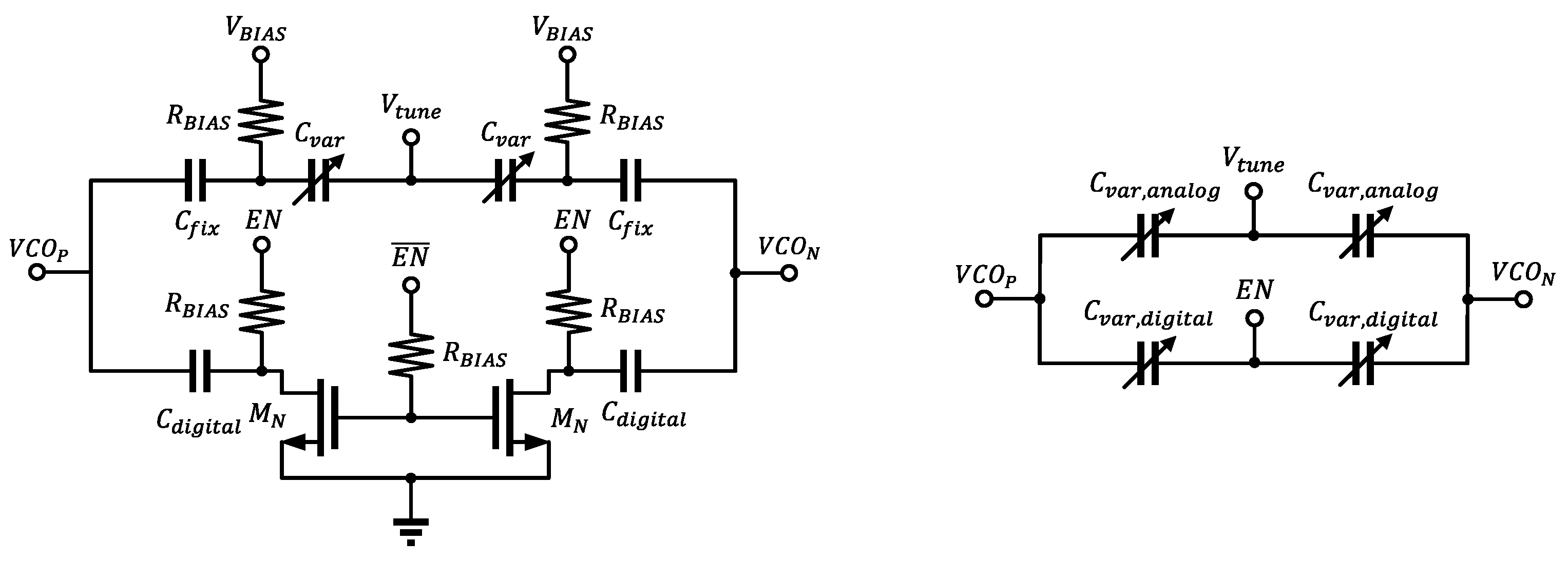
Figure 2 depicts two different implementations of capacitor arrays that can be used for millimeter-wave VCO. The conventional capacitor array on the left of Figure 2 is composed of an ac-coupled varactor and a high-Q capacitor that is switched on or off. The ac-coupled capacitor array benefits from a configuration where one side of the varactor is at the fixed dc-bias ( V B I A S ), while the other side can be tuned with analog voltage ( V t u n e ). However, due to the same configuration, the effective capacitance is reduced to C f i x C v a r and thus suffers from a reduced tuning range and more parasitics. The capacitor ( C d i g i t a l ) for digital control can utilize high-Q capacitors such as MIM (metal-insulator-metal) and MOM (metal-oxide-metal) capacitors but requires complementary switching circuits with transistors and capacitors. Then, although the capacitor itself may provide superior performance to the varactor, additional circuitries degrade the performance of its tuning range, noise, and area.
To resolve the aforementioned issues as well as to support the high-frequency K-band operation, our proposed capacitor array utilizes only the varactors in its analog tuning ( V t u n e ) and digital tuning ( EN ), which is shown in Figure 2 (right). The varactors implemented in our VCO are based on the accumulation mode varactor, with its detailed behavior described in [9]. The number of fingers and the dimensions are carefully investigated to offer the best quality factor.
With digital tuning ( EN ), the actual tuning range is determined by the value of the minimum- and maximum-capacitances of the varactor. With the compact configuration, void of transistors and resistors, the proposed capacitor array occupies less area and incurs less noise for the VCO. For the case of analog tuning ( V t u n e ), the varactors are dc-coupled to the output node and thus provide a better tuning range than the conventional one.

3. Circuit Implementation

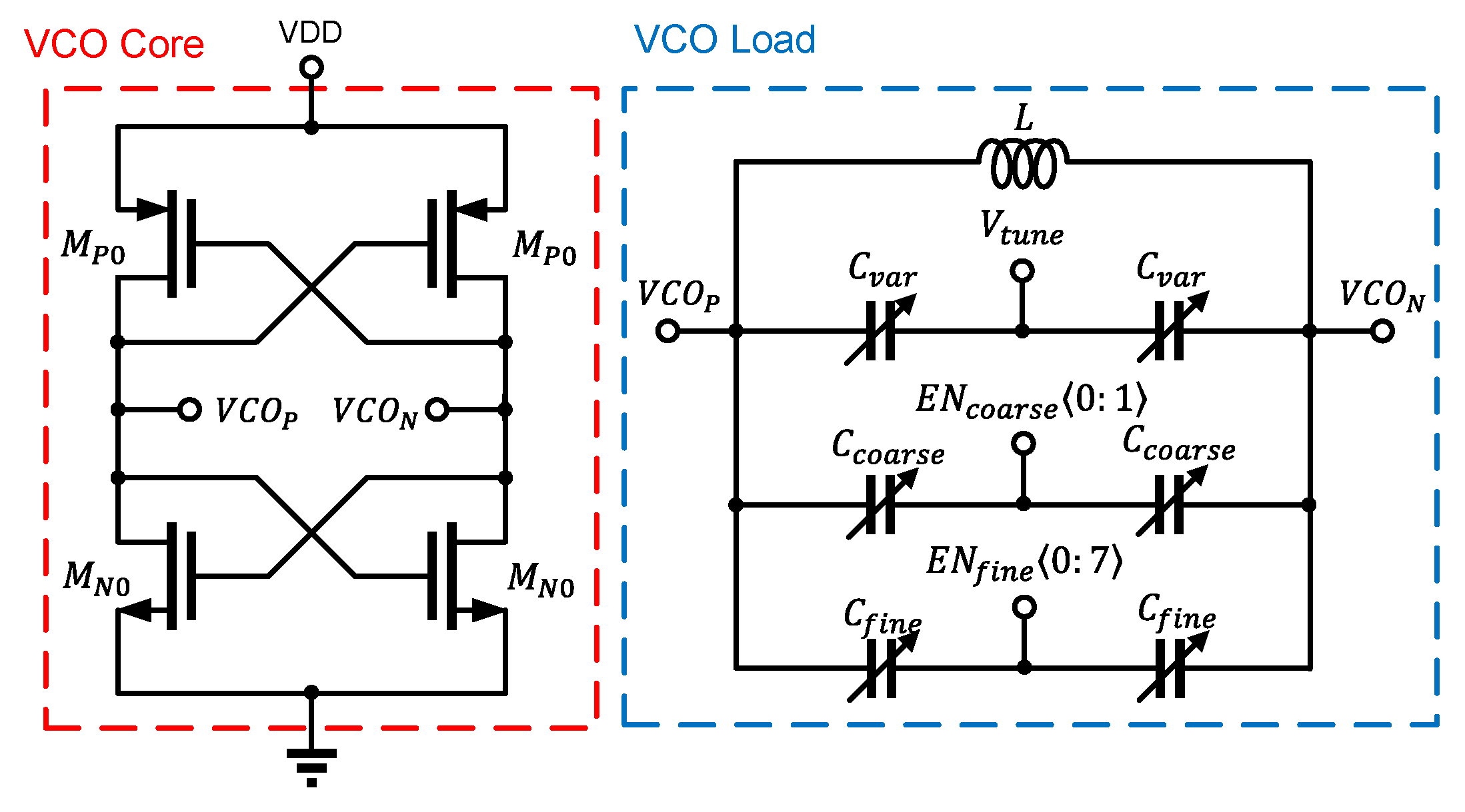
Figure 3 shows the detailed schematic of the proposed VCO. CMOS (Complementary Metal-Oxide-Semiconductor) cross-coupled pairs without a tail current are used to offer negative resistance with minimum parasitics at a millimeter-wave frequency range. An ultra-thick top metal (M9) is used to implement the inductor. From the simulation results, the inductance and quality factor of the implemented inductor is 100 pH and 30 at 18 GHz frequency, respectively.
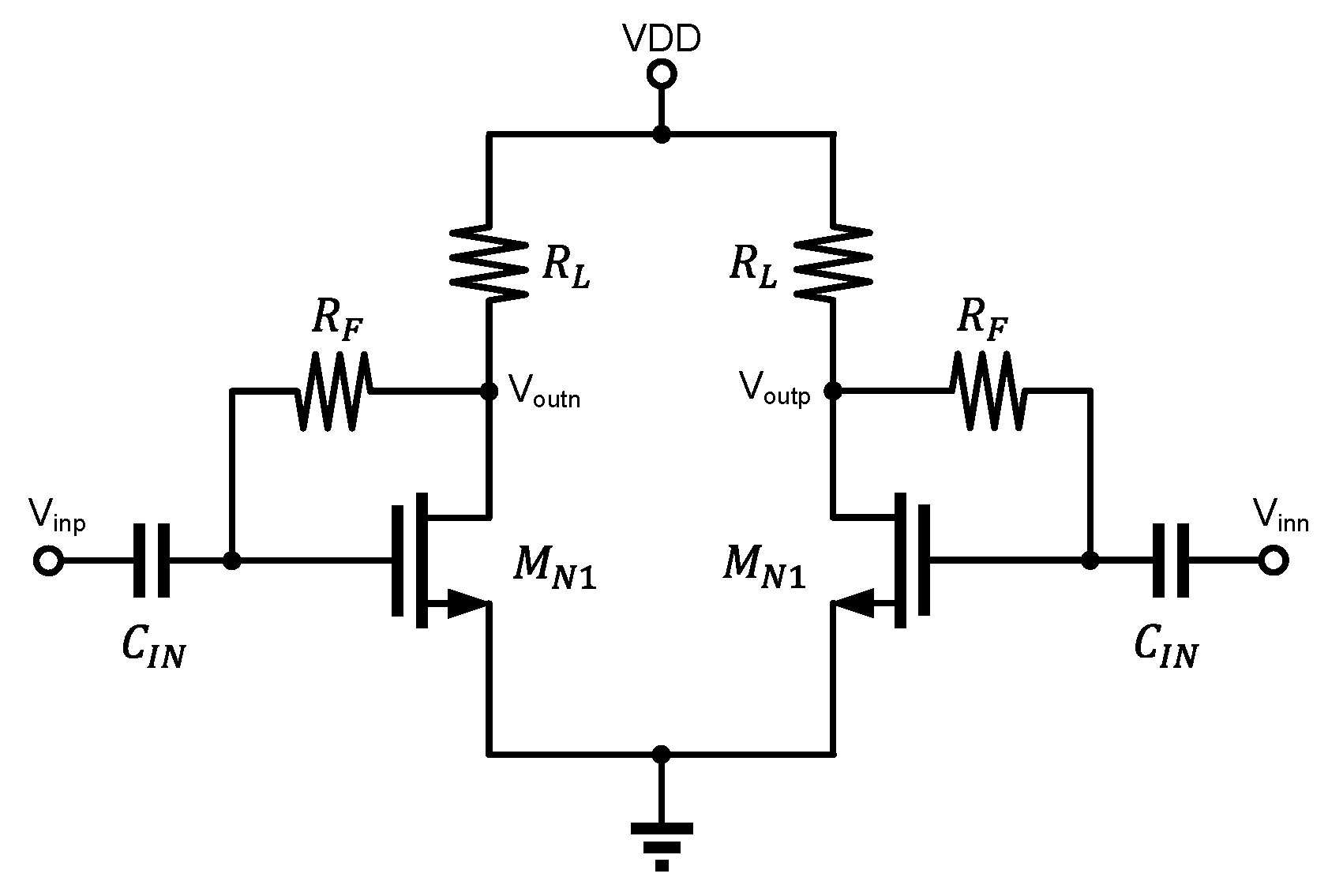
The output of the VCO is delivered to the shunt-feedback output buffer in order to provide the impedance-matched interface ( 50   Ω ) to the off-chip. The adopted buffer topology shown in Figure 4 provides broadband operation and low harmonic distortions with minimal loading effect to the VCO [10]. Furthermore, a real impedance can be provided across a wide frequency range. Neglecting the parasitic components, the shunt-feedback buffer stage provides the output resistance of
R o u t = R S + R F 1 + g m R S ,
where g m and R S are the small-signal trans-conductance of the core transistor ( M N 1 ) and the effective output resistance of the VCO (previous stage).
Using the open-circuit time-constant method [11], there are three time-constants in the circuit due to C I N , C O U T , and C F that contribute to the signal attenuation. Since the output resistance is dominated by the port impedance of 50   Ω , the dominant time constants are from C I N to C F . The former is dictated by a large effective capacitance due to the Miller effect [10], and the latter is dictated by the large effective resistance that is expressed as
R e f f = R S + R S + g m R S R L g m R S R L ,
In our designed buffer, the 3-dB bandwidth of the buffer is simulated to be 17 GHz, where the contribution due to C I N is the most dominant.

4. Simulation Results

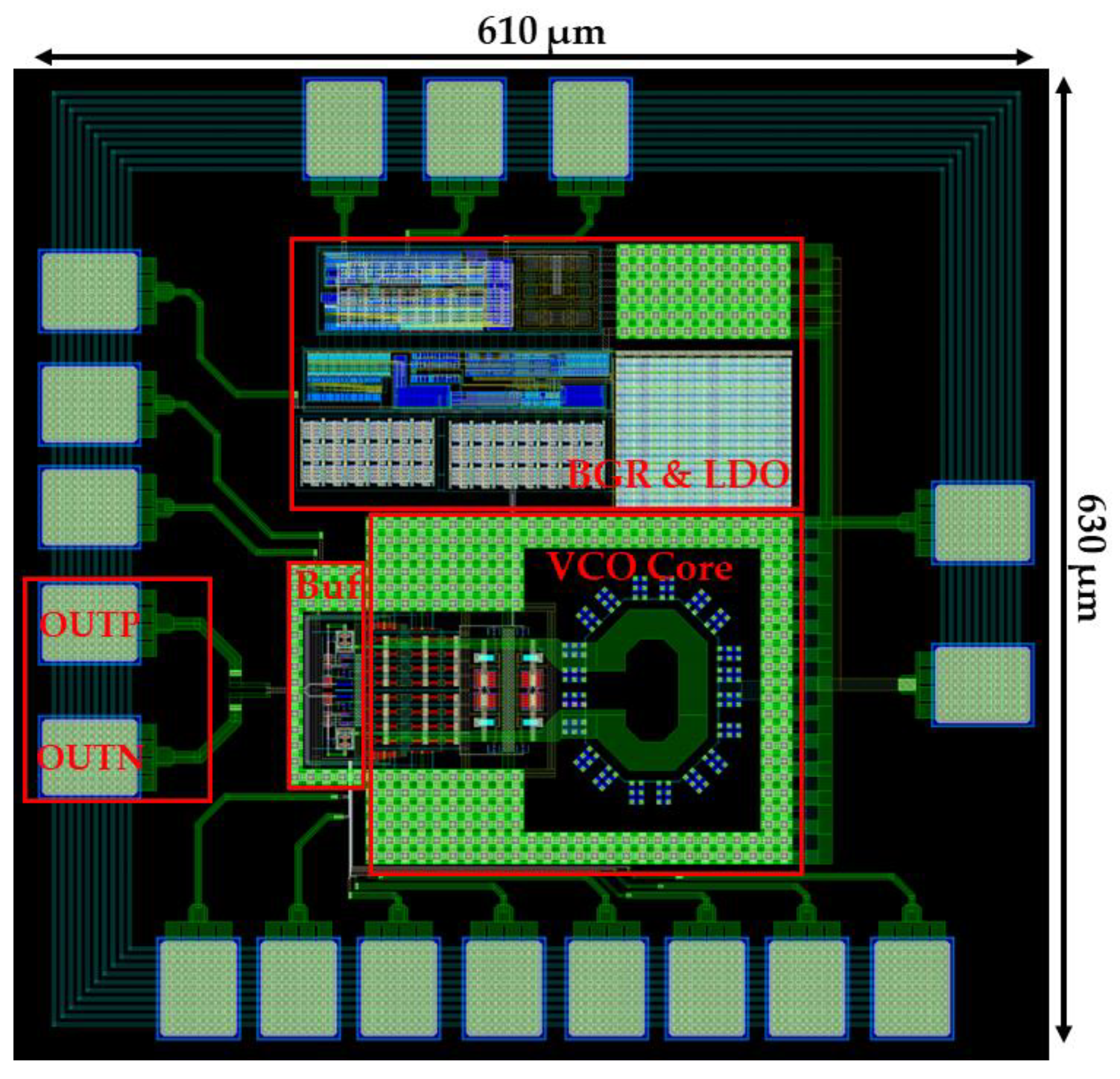
The proposed LC VCO is implemented using a 65 nm CMOS process and its device dimensions for the VCO core circuit as well as a shunt-feedback buffer are indicated in Table 1. A unit finger width of 2 μ m is unanimously used for all the active devices (transistors), which gives the best transistor speed [12]. The chip layout is illustrated in Figure 5. The total area of the chip is 610 × 630 μ m 2 , including the VCO core, on-chip bias circuits (bandgap reference and regulator), shunt-feedback buffer to interface the VCO outputs to off-chip ports, and pads. The active area of the VCO core is only 270 × 220 μ m 2 .
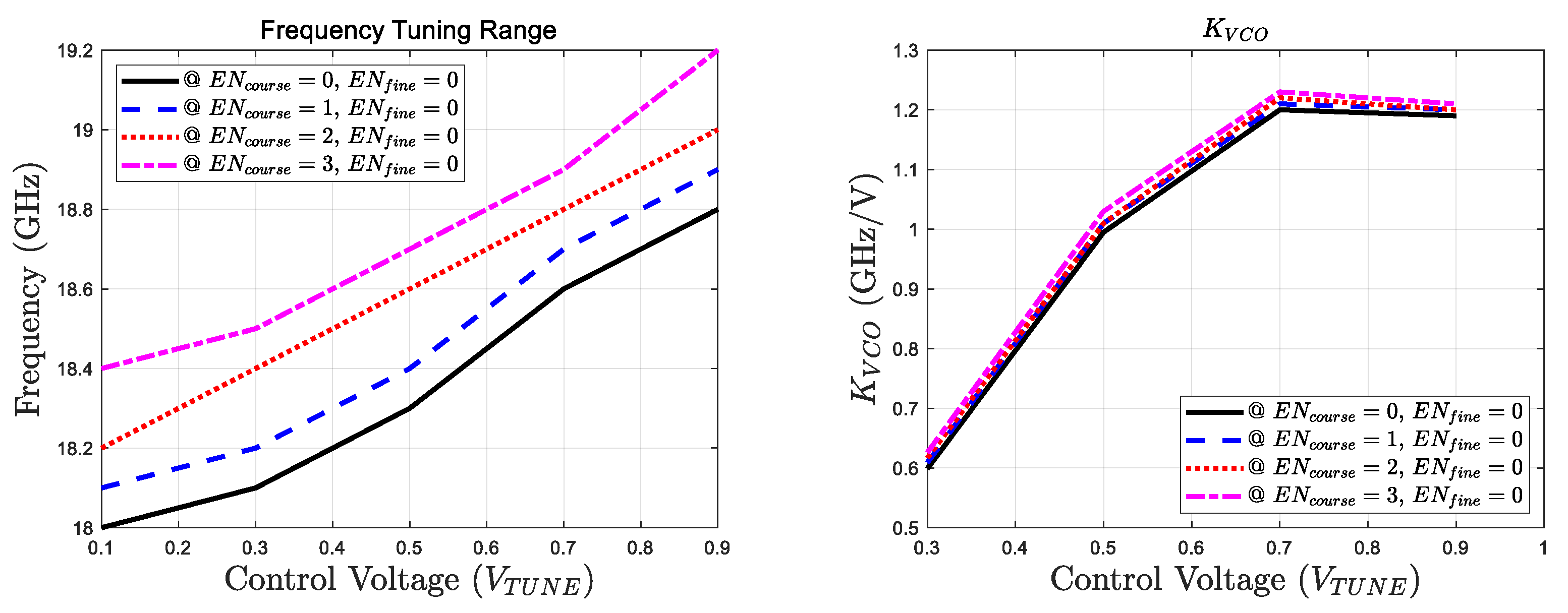
The proposed VCO is equipped with a fixed inductor ( L ) of 100 pH along with a varactor ( C v a r ), fine-tuning capacitor ( C f i n e ), and coarse-tuning capacitor ( C c o a r s e ), whose dimensions are illustrated in Table 1. C f i n e is controlled by a 7-bit thermometer code to ensure the monotonic response in the VCO oscillation frequency, while C c o a r s e is switched on/off by 2-bit binary code. The oscillation frequency of the VCO varies from 18 GHz to 19.2 GHz when it is simulated with E N c o a r s e = 0 ,     E N f i n e = 0 ,     V t u n e = 0.1   V and E N c o a r s e = 3 ,     E N f i n e = 255 ,     V t u n e = 0.9   V , respectively. Figure 6 shows the frequency tuning range and K V C O for the different settings of the coarse-tuning capacitor settings and varactor control voltages ( V t u n e ).
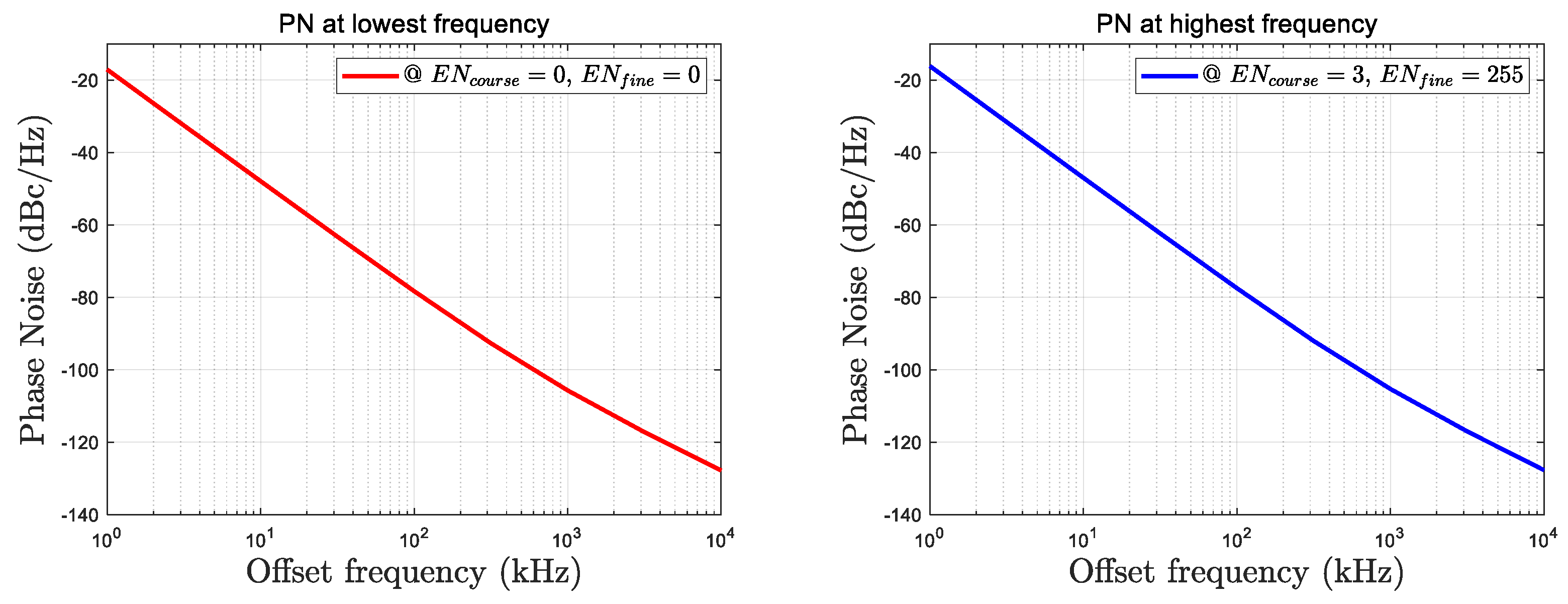
The phase noise performance of the proposed VCO is simulated at both the lowest and highest digital code settings. As shown in Figure 7, the phase noise of the VCO is consistent across the codes, and the degradation in phase noise is less than 0.5 dB. Figure 8 shows the phase noise of the VCO at 1- and 10-MHz offset frequencies across the change in control voltage ( V T U N E ). At the offset frequency of 1 MHz, the PN varies from −105.9 to −104.9 dBc/Hz, while at the offset frequency of 10 MHz, the PN varies from −128 to −127.3 dBc. The simulated PN versus control voltage is consistent and varies less than 1 dB. This result shows that the tuning capacitor, varactor ( C v a r ), exhibits stable and consistent quality factors across the control range.
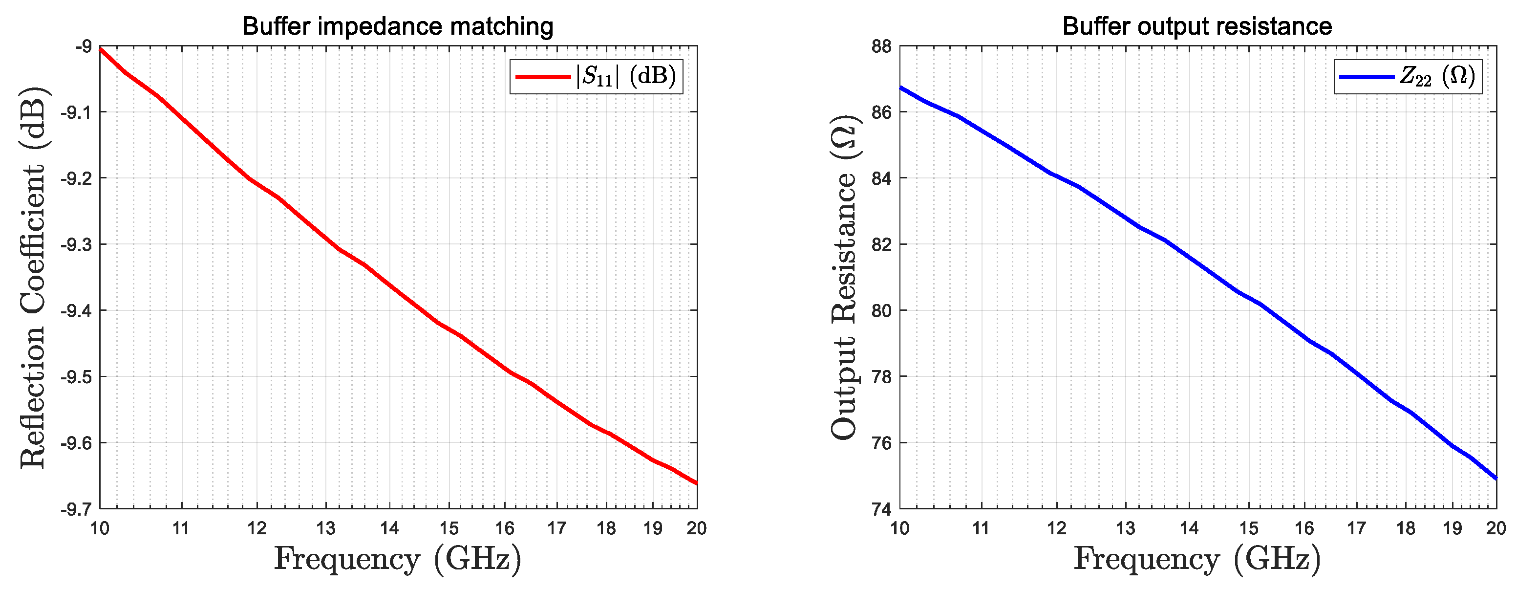
As described earlier, a shunt feedback buffer provides stable and broadband real impedance at its output port and thus can be connected to the output port without any off-chip components. The void of additional off-chip components results in a small form factor of the test board and a low bill of material (BOM). Figure 9 shows the simulated matching performance of the buffer. Across the VCO oscillation frequency range (18–19.2 GHz), the output matching ( | S 11 | ) is less than −9 dB, while the output resistance (real impedance) is less than 77   Ω .
To compare the performance of our proposed VCO with the state-of-the-art VCO at a similar frequency range, a well-known figure of merit (FoM) of the VCO defined as below is utilized:
F o M = L { f } 20 l o g ( f 0 f ) + 10 l o g ( P D C 1 m W ) ,
where L { f } is the phase noise at offset ( f ) from the carrier frequency ( f 0 ), and P D C is the power consumption. From 1 MHz offset with 19.2 GHz carrier frequency, an FoM of −178.34 dBc/Hz is achieved.
Table 2 shows the overall results and compares the performance of the proposed VCO with previous works. Reference [13] proposed a VCO with a varactor and switched substrate-shield inductor tuning; at 1 MHz frequency offset, our work achieved 6.94 dBc/Hz better FoM. Reference [14] proposed a VCO with a varactor and triple-coupled inductors, and references [1] and [15] proposed a VCO using a varactor and MIM capacitor for tuning; they achieved a similar FoM with a price of a larger area while our work only occupies 0.059 mm2 of area for the VCO core. In [16], a VCO utilizing a linearized transconductance technique is proposed, which achieves comparable performance to our design but with a wider tuning range. However, their use of an inductor in the coarse bank results in a larger area consumption compared with our approach. In contrast, while the work in [17] proposed a differential VCO with a varactor of enhanced bandwidth, our design exhibits superior performance in terms of phase noise with a 1 MHz FoM offset. Reference [2] achieved higher FoM since the proposed VCO LC tanks are realized with a high-Q capacitor array. Our work shows a fine FoM while using a varactor-only capacitor array and occupying a small chip area.

5. Conclusions

This work presents a low phase noise LC VCO that uses a varactor-only capacitor array to eliminate the detrimental effects of the conventional capacitor array. The proposed technique significantly improves the phase noise of the prototype circuit by 2 dB at 1 MHz offset frequency, and there are no significant changes in the tuning range compared to the conventional method. The differential VCO achieves a frequency range of 1.2 GHz while consuming only 21 mW of power, and its compact size of 0.378   mm 2 is a notable advantage over existing state-of-the-art oscillators that use complicated coupling transformers and tuning circuits [3,4,5,6]. Additionally, the proposed LC VCO offers a highly competitive FoM of −178.34 dBc/Hz, making it an attractive option for a range of applications where low phase noise and low power consumption are critical design considerations.

Author Contributions

Conceptualization, S.L. and J.K.; validation, J.K., H.A.A. and M.F.M.; formal analysis, K.C.; writing—original draft preparation, J.K.; writing—review and editing, H.J., S.L. and K.C.; supervision, S.L. and K.C. All authors have read and agreed to the published version of the manuscript.

Funding

This research was jointly funded by the Regional Innovation Strategy (RIS) of the National Research Foundation of Korea (NRF) funded by the Ministry of Education (MOE) (2021RIS-004) and by the National Research Foundation of Korea (NRF) grant funded by Korean Government (MIST) (No. 2022R1A4A3029433).

Data Availability Statement

Not applicable.

Acknowledgments

The EDA tool was supported by the IC Design Education Center (IDEC).

Conflicts of Interest

The authors declare no conflict of interest.

References

  1. Tan, W.; Wu, T.; Xing, Z.; Peng, Y.; Liu, H.; Kang, K. A 21.95–24.25 GHz class-C VCO for 24 GHz FMCW radar applications. In Proceedings of the 2019 IEEE MTT-S International Wireless Symposium (IWS), Guangzhou, China, 19–22 May 2019; pp. 1–3. [Google Scholar]
  2. Cho, Y.-K.; Nam, J.-W.; Lee, S.-W. A Low-Power Class-C Voltage-Controlled Oscillator With Robust Start-Up and Compact High-Q Capacitor Array. IEEE Trans. Circuits Syst. II Express Briefs 2022, 69, 819–823. [Google Scholar] [CrossRef]
  3. Yang, J.; Kim, C.Y.; Kim, D.W.; Hong, S. Design of a 24-GHz CMOS VCO With an Asymmetric-Width Transformer. IEEE Trans. Circuits Syst. II Express Briefs 2010, 57, 173–177. [Google Scholar]
  4. Kwok, K.; Luong, H.C. Ultra-low-voltage high-performance CMOS VCOs using transformer feedback. IEEE J. Solid State Circuits 2005, 40, 652–660. [Google Scholar] [CrossRef]
  5. Shahmohammadi, M.; Babaie, M.; Staszewski, R.B. A 1/f noise upconversion reduction technique for voltage-biased RF CMOS oscillators. IEEE J. Solid State Circuits 2016, 51, 2610–2624. [Google Scholar] [CrossRef] [Green Version]
  6. Hu, Y.; Siriburanon, T.; Staszewski, R.B. Oscillator flicker phase noise: A tutorial. IEEE Trans. Circuits Syst. II Express Briefs 2021, 68, 538–544. [Google Scholar] [CrossRef]
  7. Razavi, B. RF Microelectronics, 2nd ed.; Prentice Hall Communications Engineering and Emerging Technologies Series; Prentice Hall Press: Hoboken, NJ, USA, 2011. [Google Scholar]
  8. Wang, X.; Bakkaloglu, B. A 2.4-GHz LC-Tank VCO with Minimum Supply Pushing Regulation Technique. In Proceedings of the 2007 IEEE Radio Frequency Integrated Circuits Symposium, Honolulu, HI, USA, 3–5 June 2007; pp. 303–306. [Google Scholar] [CrossRef]
  9. Teo, T.H.; Xiong, Y.Z.; Fu, J.S.; Tan, E.L. LC oscillator design at 10-GHz using substrate capacitance with scalable varactor parameters extraction technique. In Proceedings of the 2005 European Microwave Conference, Paris, France, 4–6 October 2005; pp. 1–4. [Google Scholar] [CrossRef]
  10. Havrlik, M.; Libra, M.; Poulek, V.; Kowrim, P. Analysis of Output Signal Distortion of Galvanic Isolation Circuits for Monitoring the Mains Voltage Waveform. Sensors 2022, 22, 7769. [Google Scholar] [CrossRef] [PubMed]
  11. Gray, P.R.; Hurst, P.J.; Lewis, S.H.; Meyer, R.G. Analysis and Design of Analog Integrated Circuits, 4th ed.; Wiley: New York, NY, USA, 2001. [Google Scholar]
  12. Doan, C.H.; Emami, S.; Niknejad, A.M.; Brodersen, R.W. Millimeter-wave CMOS design. IEEE J. Solid State Circuits 2005, 40, 144–155. [Google Scholar] [CrossRef]
  13. Agarwal, P.; Sah, S.P.; Molavi, R.; Mirabbasi, S.; Pande, P.P.; Oh, S.E.; Kim, J.H.; Heo, D. Switched Substrate-Shield-Based Low-Loss CMOS Inductors for Wide Tuning Range VCOs. IEEE Trans. Microw. Theory Tech. 2017, 65, 2964–2976. [Google Scholar] [CrossRef]
  14. Chen, Z.; Wang, M.; Chen, J.X.; Liang, W.F.; Yan, P.P.; Zhai, J.F.; Hong, W. Linear CMOS LC -VCO Based on Triple-Coupled Inductors and Its Application to 40-GHz Phase-Locked Loop. IEEE Trans. Microw. Theory Tech. 2017, 65, 2977–2989. [Google Scholar] [CrossRef]
  15. Xu, T.; Chen, J.; Du, L.; Song, C.; Gu, Q.J.; Xu, Z. An Inverted Complementary Cross-Coupled VCO to Reduce Phase Noise Sensitivity to KVCO. IEEE Microw. Wirel. Technol. Lett. 2023. [Google Scholar] [CrossRef]
  16. Hejazi, A.; Pu, Y.; Lee, K.-Y. A Design of Wide-Range and Low Phase Noise Linear Transconductance VCO with 193.76 dBc/Hz FoMT for mm-Wave 5G Transceivers. Electronics 2020, 9, 935. [Google Scholar] [CrossRef]
  17. Ullah, F.; Liu, Y.; Li, Z.; Wang, X.; Sarfraz, M.M.; Zhang, H. A Bandwidth-Enhanced Differential LC-Voltage Controlled Oscillator (LC-VCO) and Superharmonic Coupled Quadrature VCO for K-Band Applications. Electronics 2018, 7, 127. [Google Scholar] [CrossRef] [Green Version]
Figure 1. Proposed architecture: voltage-controlled oscillator (VCO) with a varactor-only capacitor array, on-chip bias (bandgap reference and low drop-out regulator), and 50   Ω terminated shunt-feedback buffer.
Electronics 12 01532 g001
Figure 2. Conceptual schematic of the capacitor arrays: conventional capacitor array (left) and proposed varactor-only capacitor array (right).
Electronics 12 01532 g002
Figure 3. Schematic of the proposed voltage-controlled oscillator (VCO) with a varactor-only capacitor array.
Electronics 12 01532 g003
Figure 4. Schematic of the 50 Ω terminated shunt-feedback buffer.
Electronics 12 01532 g004
Figure 5. Layout of the proposed chip including a voltage-controlled oscillator and 50   Ω terminated output buffer.
Electronics 12 01532 g005
Figure 6. Simulated frequency tuning range (left) and K V C O (right).
Electronics 12 01532 g006
Figure 7. Simulated phase noise (PN) at the lowest (left) and highest (right) code settings.
Electronics 12 01532 g007
Figure 8. Simulated PN at 1- and 10-MHz offsets against control voltage ( V T U N E ).
Electronics 12 01532 g008
Figure 9. Simulated buffer output impedance matching (left) and output resistance (right).
Electronics 12 01532 g009
Table 1. Device dimensions.
Device (VCO)DimensionDevice (Buffer)Dimension
MN0
MP0
( 2   μ m / 60   nm ) × 60 MN1 ( 2   μ m / 60   nm ) × 16
( 4   μ m / 60   nm ) × 60
Cvar280 fF CIN150 fF
Ccoarse27 fF RF 3.6   K Ω
Cfine15 fF RL 150   Ω
L100 pH
Table 2. Performance comparison table.
ParameterThis Work S[1] M[2] M[3] M[13] M[14] M[15] M[16] S[17] M
Frequency
[GHz]
18–19.221.9–24.219.3–2224.2721–31.620.8518.7–20.313–1925.5
PN @ 1 MHz
[dBc/Hz]
−105.9−100.8−106.3−100.3−89.5−100.7−107.24−110−96
V D D
[V]
1110.65111.80.81.2
Power
[mW]
2183.87.84.18.123.42412
Area
[ mm 2 ]
0.378 a
0.0596 b
0.19 b0.06 b0.42 a0.25 a0.48 a0.19 b0.14 b0.45 a
FOM
[dBc/Hz]
−178.34−179.4−186.4−179.11−171.4−178−179−181.3−173.3
Technology65 nm
CMOS
65 nm
CMOS
65 nm
CMOS
40 nm CMOS65 nm bulk CMOS90 nm CMOS28 nm CMOS40 nm CMOS0.13 μm SiGe
BiCMOS
S: Simulated result. M: Measurement result. a: Total area. b: Active area.
Disclaimer/Publisher’s Note: The statements, opinions and data contained in all publications are solely those of the individual author(s) and contributor(s) and not of MDPI and/or the editor(s). MDPI and/or the editor(s) disclaim responsibility for any injury to people or property resulting from any ideas, methods, instructions or products referred to in the content.