Article

Fully Integrated 1.8 V Output 300 mA Load LDO with Fast Transient Response

1
Institute of Microelectronics of the Chinese Academy of Sciences, Beijing 100029, China
2
University of Chinese Academy of Sciences, Beijing 100049, China
3
Key Laboratory of Science and Technology on Silicon Devices, Chinese Academy of Sciences, Beijing 100029, China
*
Author to whom correspondence should be addressed.
Electronics 2023, 12(6), 1409; https://doi.org/10.3390/electronics12061409
Submission received: 16 February 2023 / Revised: 10 March 2023 / Accepted: 14 March 2023 / Published: 15 March 2023

Abstract

:
Based on an 0.18 μm process, this paper proposes a fully integrated 1.8 V output 300 mA load low-dropout linear regulator (LDO) with a fast transient response. By inserting a transient-enhanced biased Class AB super source follower at the gate of the output power transistor, this LDO can quickly adjust the gate voltage of the power transistor without additional power consumption. By adding an active capacitor circuit composed of a fast comparator with offset voltage at the output point, this LDO can quickly charge/discharge the transient current and accelerate the transient response without reducing the circuit stability. Simulation results show that the proposed LDO has an output voltage of 1.8 V, when the input voltage is 2 V to 5 V while consuming 66.4 μA of quiescent current. The proposed capless LDO has a 1.94 µV/mA load regulation, a 0.55 mV/V linear regulation, and a −60 dB@1 kHz power supply rejection. When the load current steps from 3 mA to 300 mA in 300 ns, the LDO settles in 400 ns with an overshoot and undershoot of 67 mV and 86 mV, respectively.

1. Introduction

Power management integrated circuits (PMICs) provide highly integrated, high-performance power management solutions for a wide range of applications including automotive, consumer, and telecom electronics [1,2,3,4]. The low-dropout linear regulator (LDO) is one of the important branches of PMICs, which can generate stable, low noise, and accurate output voltage from the battery [5,6,7,8]. To prolong battery life and improve power efficiency and stability, LDOs need to minimize quiescent current and voltage drop while maintaining good regulation, load capability, and fast transient response, which are major concerns in LDO design [9,10,11,12].
Traditional LDO regulators use large off-chip capacitors to obtain good transient performance, but this kind of LDO has the disadvantages of large chip area, high cost, and is not conducive to realizing fully integrated chips [13,14,15,16]. However, in fully integrated LDOs, the transient response and stability are significantly reduced due to the absence of the off-chip capacitor, thus becoming the major design challenge [17,18,19,20,21].
In order to solve the above problems, many solutions have been proposed. For example, [22] proposed an adaptive transient current distribution technique to accelerate the transient response of LDO without off-chip capacitors. However, the threshold of the inverter used to detect the overshoot/undershoot voltage was easily affected by the power supply voltage and process fluctuations, and the load capacity of this design was only 10 mA. The authors in [23] used a digital circuit to realize the transient enhancement of LDO, but the quiescent current of 495 μA was too high, which was not suitable for short-life battery-powered equipment. The authors of [24] inserted a transient enhancement circuit from the drain to the gate of the power output transistor to make it AC-coupled and performed frequency compensation on the high slew rate error amplifier to achieve the stability of LDO and improve the load capacity without an off-chip capacitor. However, the overshoot and undershoot voltages were 170 mV and 234 mV, which needed further optimization. In other solutions, such as those found in [25,26], the transient response was improved by using adaptive biasing, but circuit complexity and power consumption were increased. Additionally, some LDOs required a minimum load current to be stable, as in [27,28], resulting in increased power consumption and light-load stability issues. The authors of [29] propose an LDO based entirely on on-chip FVF. Double buffers were inserted into the cascode flipped voltage follower (FVF) topology for better power supply rejection (PSR) and reduced voltage variation during load transients. However, the maximum load current of this design is 10 mA, while the quiescent current is 100 μA, and the load regulation rate is 1.21 mV/mA, which needs further optimization. In addition to performing transient compensation on the gate of the power transistor, the authors of [30,31] propose a current mirror-based active capacitor structure for transient enhancement at the LDO output, but this structure lacks large current and capacitive load capacity. In short, designing a fully integrated LDO with a strong load capacity and good transient performance requires a trade-off between power consumption, load capacity, transient characteristics, and stability [32,33,34,35].
In this paper, a 300 mA load, fully integrated, low-dropout regulator with a fast transient response is presented. A transient enhanced biased Class AB super source follower structure is proposed to dynamically increase the slew rate and improve stability. Additionally, an active capacitor circuit composed of a fast comparator with offset voltage is proposed, which can inject/sink current to/from the output point to further enhance the transient response. Additionally, this design incorporates a temperature and voltage-independent reference voltage source to realize truly integrated devices. This paper is organized as follows: Section 2 presents the proposed transient enhancement technique and the design of the proposed LDO. Section 3 reports simulation results and comparisons with other LDO. Finally, Section 4 draws conclusions.

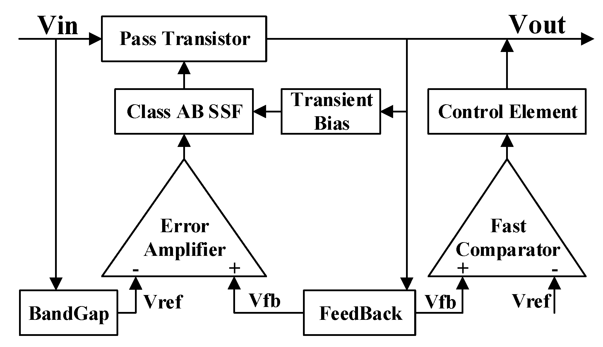
2. Proposed Transient Enhancement Technology and Fully Integrated LDO

The structure of the proposed LDO is shown in Figure 1. The input power V i n from the battery is regulated by a multi-loop regulator to output a stable voltage V o u t . The main regulation loop consists of the feedback resistor, bandgap reference, error amplifier, source follower, and pass transistor. The function of the feedback resistor is to sense the variations over V o u t due to the variations of the supply voltage/load current. The error amplifier is responsible for comparing the feedback voltage V f b with the reference voltage V r e f and controlling the pass transistor to make necessary modifications to the output voltage to maintain it at the desired voltage.
Based on the main regulation loop described above, a transient-enhanced biased Class AB super source follower (TEB Class AB SSF) is proposed in this design. Compared with traditional source followers, this structure has a higher slew rate and a transient-enhanced bias current to achieve a faster transient response at the gate of the power transistor. Additionally, this paper proposes an active capacitor structure for transient enhancement of the output point by using a fast comparator with offset voltage and higher bandwidth to quickly drive the control element to sink/source current to/from the output during transients without affecting the operation of the circuit under static conditions. This structure can further accelerate transient performance without compromising circuit stability.

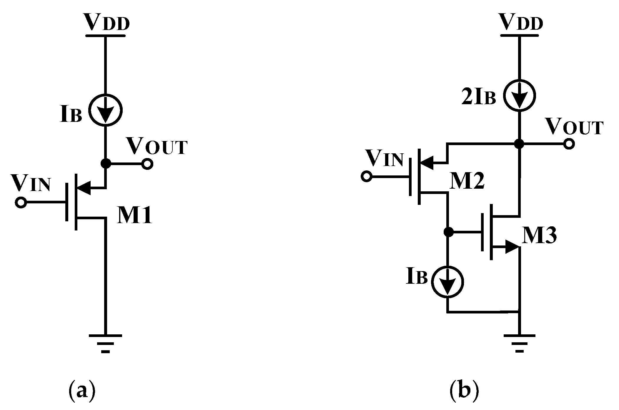
2.1. Transient-Enhanced Biased Class AB Super Source Follower

In order to provide a load current of 300 mA, the size of the pass transistor of the LDO needs to be large so that the gate-source parasitic capacitance will also be large. In order to make the load regulation and linear regulation meet the design requirements, the error amplifier is required to have a higher gain, thus increasing the output resistance. If the output of the error amplifier were connected directly to the gate of the pass transistor, a very low-frequency pole would be created, affecting the stability of the circuit at light loads. In addition, the charge and discharge slew rate of the gate-source parasitic capacitance of the pass transistor is limited by the tail current source of the error amplifier. Therefore, a source follower should be inserted between the output of the error amplifier and the gate of the pass transistor to lower the resistance and separate the pole into high frequencies while increasing the slew rate [36]. The commonly used source follower is the single-transistor source follower and the super source follower is shown in Figure 2.
The PMOS source follower in Figure 2a is a widely used Class A voltage buffer. Although this structure can quickly absorb the current from the gate-source parasitic capacitance and has a simple structure, the maximum current it can provide is limited by the bias current I B . The maximum positive slew rate (SR) is I B / C P A S S , where C P A S S is the gate capacitance of the pass transistor. In addition, as shown in the following expression, the output resistance R O U T 1 is still large.
A V 1 = 1 1 + g m b 1 / g m 1 + 1 / g m 1 r o 1
R O U T 1 = 1 g m 1 + g m b 1
The super source follower in Figure 2b can reduce the output resistance due to the addition of M 3 , while ensuring that the transfer function is almost unchanged. However, this structure is still a Class A working mode, and the positive slew rate is still limited by the bias current.
A V 2 = 1 1 + g m b 2 / g m 2 + 1 / g m 2 r o 2 + 1 / g m 2 r o 2 g m 3 r o 3
R O U T 2 = 1 ( g m 2 + g m b 2 ) g m 3 r o 2 / / r o 2 I B
Based on quasi-floating gate technology [36,37,38], this paper proposes a Class AB super source follower with a transient-enhanced bias to solve the problem of positive slew rate limitation and improve transient response. The circuit diagram is shown in Figure 3a, where V I is connected to the output of the error amplifier, and V O is connected to the gate of the pass transistor.
It works as follows, a high-pass filter composed of a large impedance M T 1 , pseudo-resistor, and C 1 is inserted into the super source follower. Thus, node A becomes a quasi-floating gate (QFG) node [39,40]. Without increasing the quiescent current, C 1 couples the AC variations of node C to node A with an attenuation equivalent to α = C 1 / ( C G S 6 + C 1 ) , where C G S 6 is the parasitic capacitance at the gate of   M S 6 . The minimum frequency of the AC signal that can be coupled to node A is the cut-off frequency 1 / 2 π R T 1 C 1 of the high-pass filter, where R T 1 is the equivalent impedance of the diode-connected MOS transistor operating at the cut-off region, which is on the order of giga-ohms. So that the cut-off frequency is usually lower than 1 Hz, only the DC voltage is not transmitted. This structure enables the M S 6 and M S 8 to behave as Class AB push–pull output stages during dynamic operation, addressing the positive slew rate limitation of the traditional structures. For example, when V I is a positive input swing, V O is a positive swing, and the drain of M S 7 is a negative swing. C 1 couples the change at the drain of M S 7 to the gate of M S 6 , and the current of M S 6 is transiently increased, thereby increasing the positive slew rate. The DC transfer function and output resistance expressions of this structure are as follows:
A V 3 = 1 1 + g m b s 7 / g m s 7 + 1 / g m s 7 r o s 7 + 1 / g m s 7 r o s 3 / / r o s 7 g m s 8 + α g m s 6 + β g m s 3 ) ( r o s 6 / / r o s 8
R O U T 3 = 1 ( g m s 7 + g m b s 7 ) g m s 8 + α g m s 6 + β g m s 3 r o s 7 / / r o s 6
where β = C 2 / ( C G S 3 + C 2 ) , and C G S 3 is the parasitic capacitance at the gate of M S 3 . Figure 3b shows the slew rate simulation results. It can be seen that the positive (SR+) and negative (SR−) slew rates of the proposed TEB Class AB SSF are 43.61 V/μs and 88.26 V/μs, respectively. Compared with the traditional structure, the slew rate of this design is significantly improved, which solves the Class A working mode of the traditional source follower.
Apart from using quasi-floating gate technology to implement the Class AB operating mode [36], this design inserts M T 2 and C 2 between the node B and the output ( V O U T ) of the LDO. In this way, a short transmission path from V O U T to node C via M S 3 is added to form a transient enhancement bias circuit. Without increasing the quiescent current, C 2 detects the change of LDO output voltage V O U T and couples it to the gate of M S 3 with an attenuation equivalent to β, which further accelerates the transient response. For example, when the load jumps from light load to heavy load, an undershoot voltage occurs, and C 2 couples the undershoot voltage to the node B, so that the drain voltage of M S 3 rises rapidly, instantly increasing the discharge current of the gate capacitance of the pass transistor. At the same time, the variation at the gate of M S 8 is coupled to the gate of M S 6 by C 1 and quickly turns off M S 6 , thereby accelerating the transient response.

2.2. Proposed Active Capacitor Circuit

In addition to the above transient enhancement structure, this paper also proposes an active capacitor circuit as shown in Figure 4. The active capacitor functions like a large-value passive capacitor at the LDO output. It instantly detects the output voltage variation and provides a transient source/sink current to suppress it under load-step changes [30,31]. Different from the active capacitor in the main loop of the LDO in [30], the active capacitor proposed in this design is only an auxiliary transient enhancement structure. This circuit consists of 12 transistors M C 1 M C 2 . When the load current jumps from heavy load to light load, the fast comparator composed of M C 1 M C 5 detects the overshoot voltage and turns on M C 6 for transient discharging. When the load jumps from light load to heavy load, the fast comparator composed of M C 7 M C 11 detects the undershoot voltage and turns on M C 12 for transient charging. Because the sizes of M C 6 and M C 12 are much smaller than the pass transistor M P , the bandwidth of the two fast comparators is greater than that of the main error amplifier, so the response speed is faster than the main loop.
By setting the input offset voltage of the fast comparator, the active capacitor circuit only operates when overshoot/undershoot occurs to avoid reducing system stability. Under dynamic conditions, when V f b V r e f + V o s , i n , M C 6 is turned on to source current from V o u t . Conversely, when V f b V r e f V o s , i n , M C 12 is turned on to sink current into V o u t . Taking the fast comparator composed of M C 1 M C 5 as an example, the input offset voltage expression is:
V O S , i n = ( V G S V T H ) m c 2 , 3 2 Δ W / L W / L m c 2 , 3 Δ V T H , m c 2 , 3 + ( V G S V T H ) m c 4 , 5 2 Δ W / L W / L m c 4 , 5 Δ V T H , m c 4 , 5 g m c 4 , 5 g m c 2 , 3
It can be seen that the input offset voltage is determined by setting the W/L of the input transistor. This structure acts as an active capacitor at V O U T , which can transiently source/sink current from/to V O U T .

2.3. Proposed Fully Integrated Low Dropout Linear Regulator with Fast Transient Response

The fully integrated LDO with a fast transient response proposed in this paper is shown in Figure 5, including the bandgap reference, the error amplifier, the class AB super source follower with transient enhanced bias, and the active capacitor circuit. Additionally, there is an enable circuit (not shown in Figure 5) for turning on/off the LDO. Bandgap references generate bias and reference voltages that are independent of power supply and temperature and provide them to other circuits. The error amplifier detects the difference between the feedback voltage V f b and the reference voltage V r e f and transmits it to the transient enhanced biased Class AB super source follower (TEB Class AB SSF). The Class AB super source follower increases the slew rate at the gate of the pass transistor and improves the transient response while reducing the impedance at this point to enhance circuit stability. The active capacitor circuit provides a fast source/sink current from/to the output point during load transients.
In order to verify the impact of the proposed transient enhancement circuits on load transient behavior, a comparative simulation is carried out in this paper, and the results are shown in Figure 6. From the simulation results, it can be seen that the proposed active capacitive circuit (A–C) and transient-enhanced biased Class AB super source follower (TEB SSF) can significantly enhance the load transient response.
To analyze the stability of the proposed LDO, the small-signal analysis model is shown in Figure 7. The active capacitor circuit is not included in the small-signal analysis because it has an offset voltage and therefore has no effect on the stability of the small-signal system. Without frequency compensation, this structure may have stability problems caused by the low frequency of the LDO output pole under light load. To solve this problem, this design adopts the nested Miller compensation technology composed of the gate parasitic capacitance C gd of the power transistor and the Miller capacitance C C to stabilize the system. The transfer function of the proposed LDO is derived as follows:
V O U T V I N = g m E R 1 g m B R 2 g m P R L 1 s C C 1 / g m P R C 1 + s R 1 1 + g m B R 2 g m P R L C C + C 1 , t o t 1 + s R 2 C 2 + 1 + g m P R L C g d 1 + s C L 1 / g m P
where g m E , g m B g m S 7 / g m S 7 + g m b S 7 R O U T 3 , and g m P are the transconductance of the error amplifier, buffer, and the power transistor, respectively. R 1 = g m E 9 r o E 9 r o E 11 / / g m E 7 r o E 7 r o E 5 / / r o E 3 and C 1 , t o t = C 1 + 1 + g m P R O U T C C are the resistance and capacitance of node V 1 , where C 1 = C g s , S 7 and R O U T = r o P / / R L . R 2 = R O U T 3 and C 2 = C g s P + 1 + g m P R O U T C g d P are the resistance and capacitance of node V 2 . C C and R C are the Miller compensation capacitor and zeroing resistor, and C g d P is the parasitic capacitance of the power transistor. It can be obtained from the analysis that the expressions of the zeros and poles of the circuit are as follows:
p 1 = 1 R 1 1 + g m B R 2 g m P R L C C + C 1 , t o t
p 2 = g m P C L
p 3 = 1 R 2 C 2 + 1 + g m P R L C g d
z 1 = g m P C C 1 g m P R C
It can be obtained from the analysis that the dominant pole p 1 is at the output of the error amplifier. The p 2 non-dominant pole is located at the output of the LDO, and the frequency of this pole varies with the load capacitance. The gate of the pass transistor is the non-dominant pole p 3 . Because this design uses a transient-enhanced biased Class AB super source follower with extremely small output resistance, the frequency of p 3 is outside UBW even under extreme conditions. In addition, the zeroing resistor R C makes the zero z 1 located in the left half plane, which offsets the influence of the pole p 2 and enhances the stability of the system.
In order to verify the stability of the proposed LDO, the stability of the LDO under different load conditions is simulated, and the results are shown in Figure 8. It can be seen that when the load capacitance is 0 pF and the load current changes from 0 to 300 mA, the phase margin (PM) of the proposed LDO is 70.1 deg@0 mA, 71.5 deg@100 μA, 72.8 deg@1 mA, 73.6 deg@100 mA, and 79.8 deg@300 mA. When the load current is 1 mA and the load capacitance changes from 0 to 100 nF, the phase margin of the proposed LDO is 72.8 deg@0 pF, 71.35 deg@100 pF, 67.71@1 nF, 54.45@10 nF, and 48.73@100nF. Therefore, the proposed LDO has good stability under all load conditions.

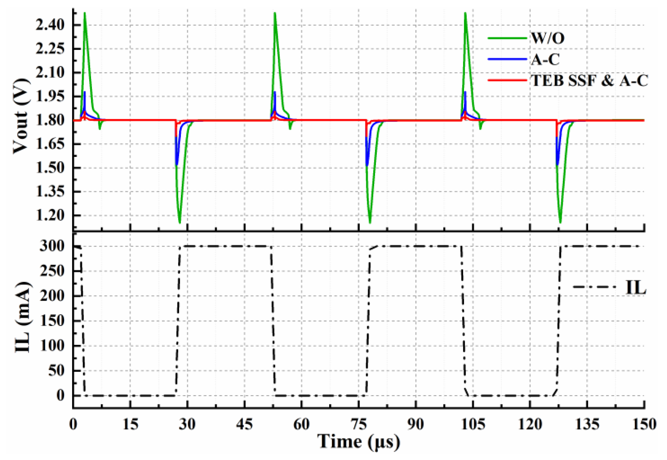
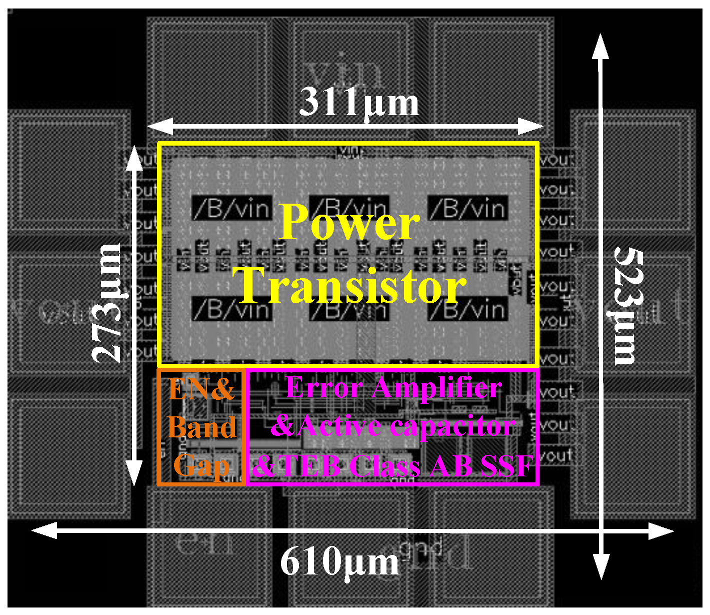
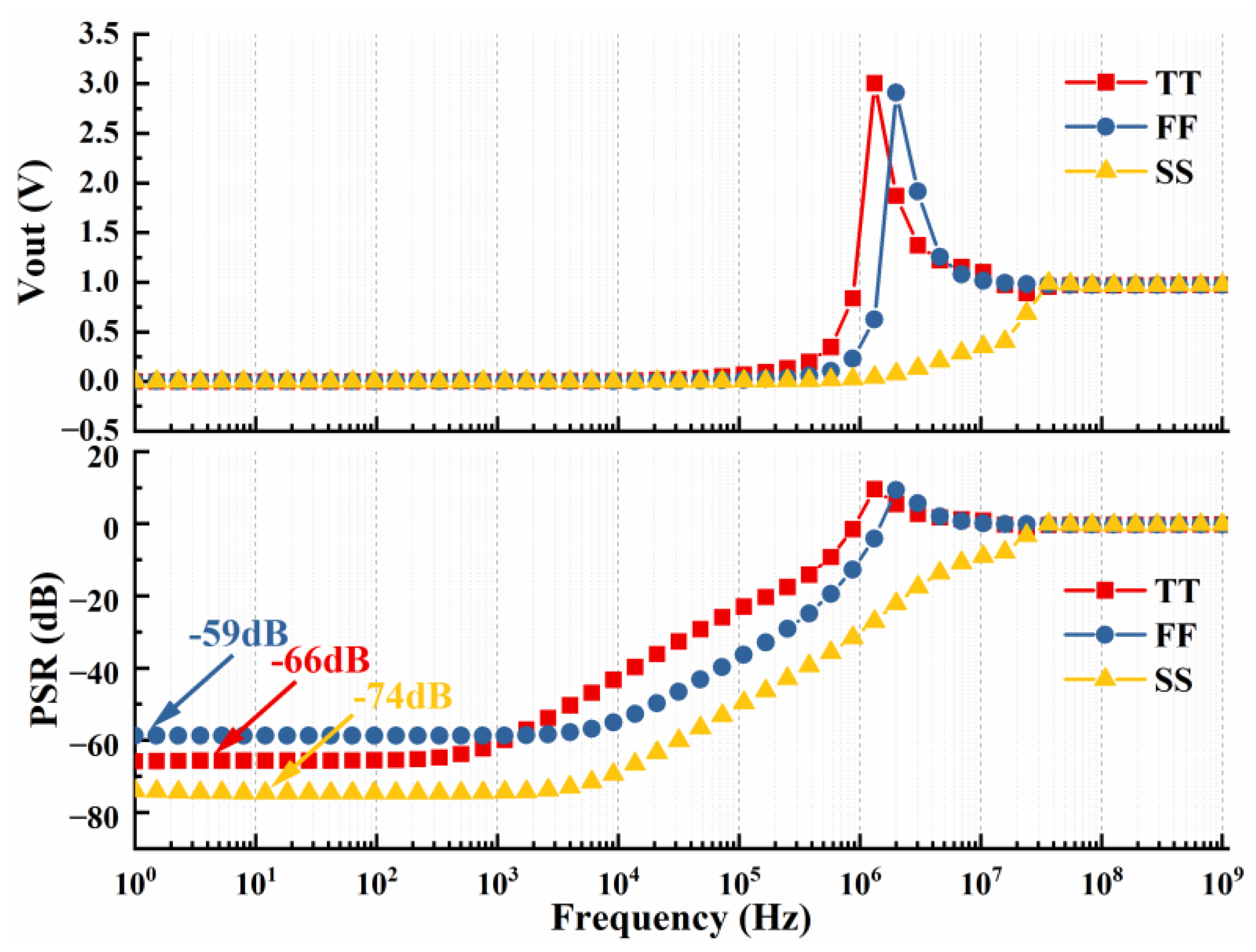
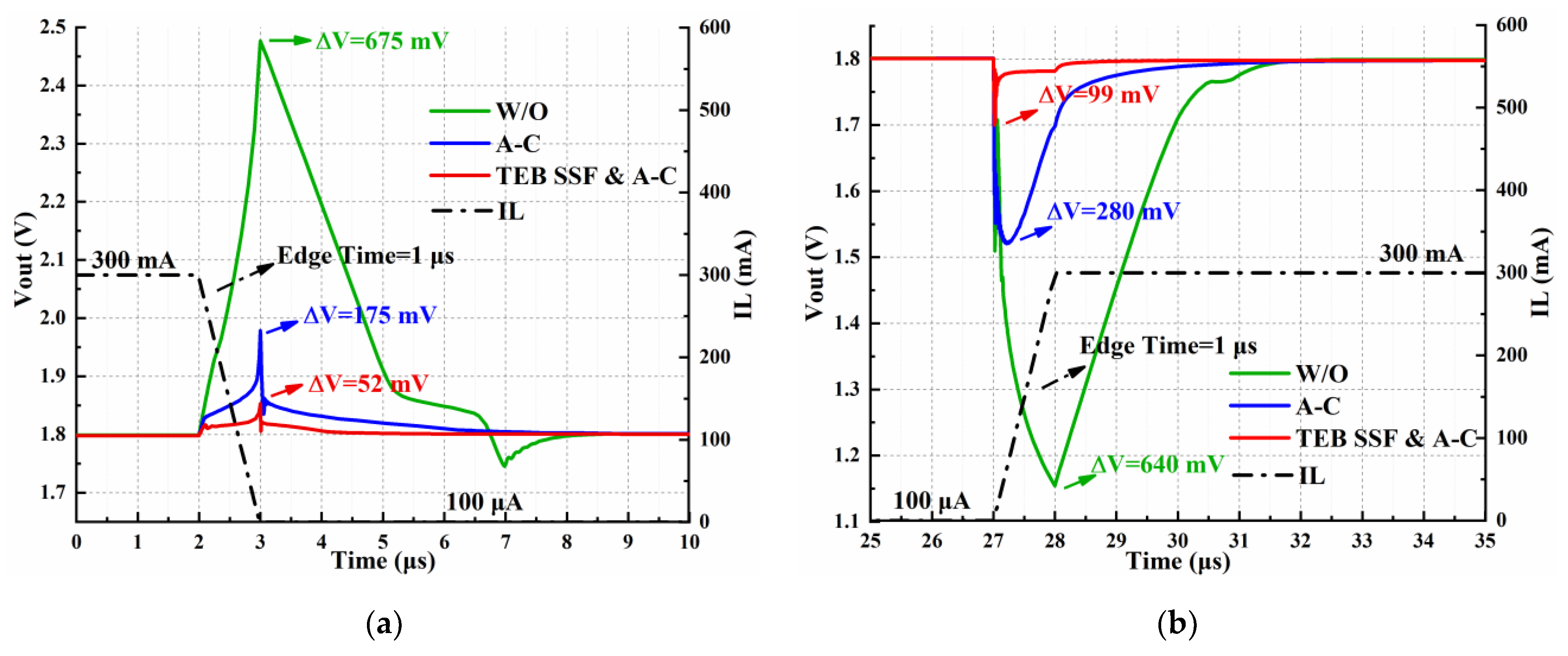
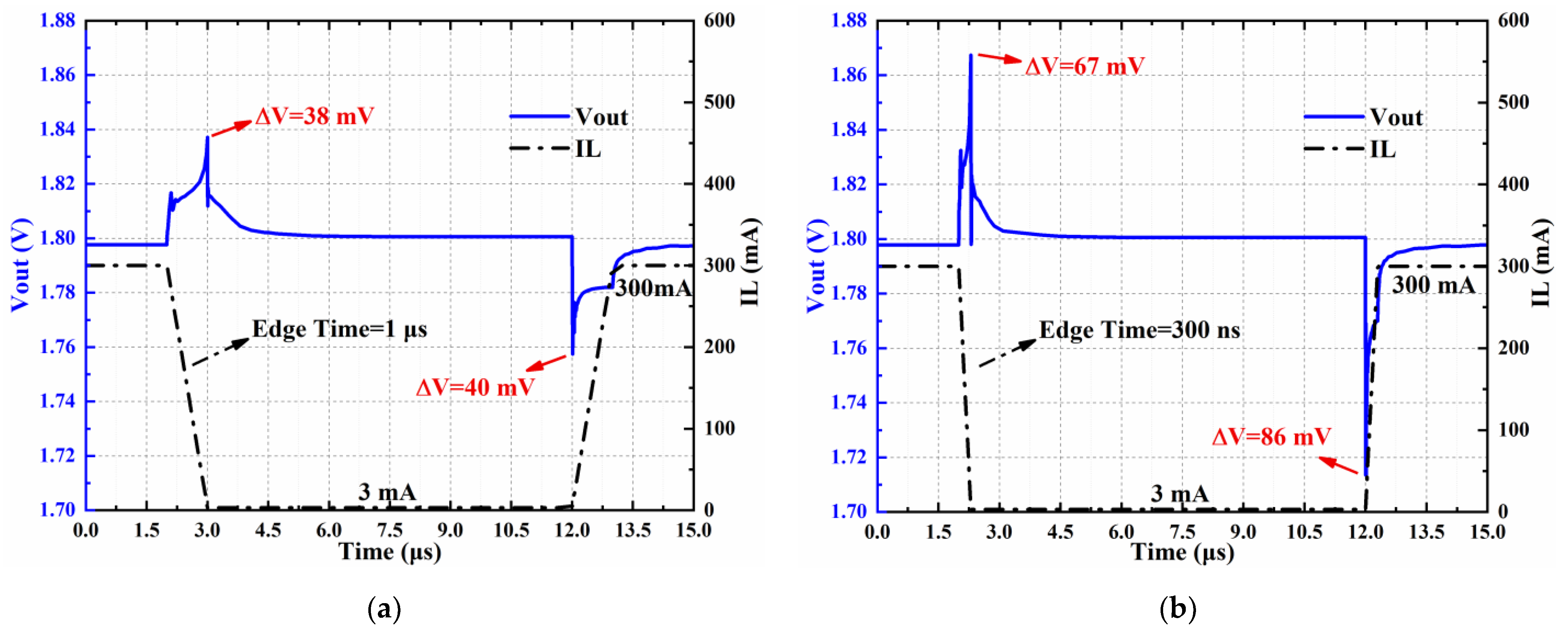
3. Layout and Simulation Results

The proposed LDO is designed on a 0.18 μm BCD process. Figure 9 shows the layout of this design, with an overall area of 610 µm × 523 µm (including pads). This design includes an enable circuit, a bandgap reference, an error amplifier, an active capacitor circuit, a transient-enhanced biased Class AB super source follower, and the power transistor. The designed circuit is simulated by Cadence Spectre, and the simulation results are shown as follows.
Figure 10a shows the simulation results of linear regulation and dropout voltage under different process corners. It can be seen that the proposed LDO has a constant output of 1.8 V, a dropout voltage of 200 mV, and a linear regulation of 0.55 mV/V when the input voltage ranges from 2 V to 5 V (IL = 100 mA). Figure 10b presents the simulation results of load regulation under different process corners. It can be seen that when the load current changes from 0 to 300 mA (Vin = 3.3 V), the load regulation is 1.94 µV/mA.
Figure 11 shows the simulation results of power supply rejection (PSR) under different process corners. It can be seen that the PSR of the proposed LDO is −66 dB@0 Hz, −60 dB@1 kHz, and −40 dB@10 kHz. Therefore, the design has good power supply rejection characteristics.
The proposed LDO can supply a maximum load current of 300 mA. As shown in Figure 12, when the load current increases from 0 to 300 mA ( V i n = 3.3 V), the ground current of the proposed LDO varies from 66.4 μA to 76.2 μA under different process corners. When the input supply voltage increases from 2 V to 5 V ( I L = 0 mA), the ground current of the proposed LDO varies from 30 μA to 100 μA under different process corners.
Figure 13 shows the transient response of the proposed LDO with and w/o active capacitors (A–C) and transient-enhanced bias Class AB super source follower (TEB SSF). The load current step is 100 μA–300 mA–100 μA, and the edge time is 1 μs. Figure 13a shows the behavior of the overshoot variations. The proposed LDO with an A–C structure can enhance the discharge process and reduce the maximum change to 175 mV within 3.5 µs. The proposed TEB SSF and A–C structure (TEB SSF and A–C) further strengthens this process and reduces the maximum change to 52 mV within 1.1 µs. Compared to an LDO without this structure, the setting time is shortened by 4.9 µs, and the overshoot voltage is reduced by 623 mV. Figure 13b shows the behavior of the undershoot variation. With the A–C circuit, the charging process can be enhanced, and the maximum change can be reduced to 280 mV within 2.5 μs. With the TEB SSF and A–C circuit, this process is enhanced to reduce the maximum change to 99 mV within 1.1 μs. Compared to an LDO without this structure, the setting time is shortened by 3.4 µs, and the undershoot voltage is reduced by 541 mV.
Figure 14 shows the load transient response simulation results of different edge times for 3–300 mA load steps. Figure 14a shows the load transient response of 3–300 mA@1 μs. The overshoot voltage is 38 mV, the undershoot voltage is 40 mV, and the setting time is 1.5 μs. Figure 14b shows the load transient response of 3–300 mA@300 ns. The overshoot voltage is 67 mV, the undershoot voltage is 86 mV, and the setting time is 400 ns.
Table 1 gives the performance summary and comparison with state-of-the-art designs. The proposed LDO provides a maximum output current of 300 mA and a regulated output voltage of 1.8 V over a supply range of 2–5 V. As can be seen from the comparison, this design has the fastest transient response and lowest load regulation with only 66.4 μA of quiescent current and without off-chip capacitors. This indicates that the proposed transient enhancement circuit structure can achieve a faster transient response and a more accurate output voltage.
To compare various regulators implemented in different technologies, an F O M is adopted from [2]:
F O M = K × C T O T × Δ V o u t × I Q Δ I L O A D 2
K = Δ t   used   in   the   design   the   smallest   Δ t   in   the   design   for   comparison
Among them, C T O T = C L D O + C O U T , C L D O is the total capacitance used by the LDO internal circuit, and C O U T is the minimum output capacitance required when the LDO is stable. The smaller the F O M , the better the transient response achieved by the LDO. As shown in Table 1, the proposed LDO achieves the smallest F O M factor among all these designs.

4. Conclusions

This work presents a 1.8 V output, 300 mA load fully integrated LDO with a fast transient response. A transient-enhanced biased Class AB super source follower is proposed to increase the slew rate at the gate of the power transistor to improve transient response while reducing the impedance of this node to enhance circuit stability. An active capacitor circuit is proposed to provide a fast source/sink current path at the output point during load transients, thereby achieving a fast transient response. Simulation results show that the proposed LDO has a linear regulation of 0.55 mV/V and a load regulation of 1.94 μV/mA. In particular, this design has an overshoot/undershoot voltage of 52/99 mV and a settling time of 1.1 μs when the load current varied from 100 μA to 300 mA with an edge time of 1 μs. When the load current steps from 3 mA to 300 mA in 300 ns, the LDO has a settling time of 400 ns and an output overshoot and undershoot voltage of 67 mV and 86 mV, respectively, achieving a transient FOM of 0.576 fs. In summary, the proposed LDO is suitable for applications such as modern fully integrated automotive sensor chips.

Author Contributions

Conceptualization, M.G. and X.C.; methodology, M.G. and X.C.; validation, M.G. and Y.G.; formal analysis, M.G.; investigation, R.X.; resources, X.C. and B.L.; writing—original draft preparation, M.G.; writing—review and editing, M.G., X.C. and B.L.; supervision, X.C. and B.L.; project administration, X.C. and B.L.; funding acquisition, X.C. and B.L. All authors have read and agreed to the published version of the manuscript.

Funding

This work was supported by the National Natural Science Foundation of China, grant number U22B2043.

Institutional Review Board Statement

Not applicable.

Data Availability Statement

No new data were created or analyzed in this study. Data sharing is not applicable to this article.

Conflicts of Interest

The authors declare no conflict of interest.

References

  1. Hong, S.-W.; Cho, G.-H. High-Gain Wide-Bandwidth Capacitor-Less Low-Dropout Regulator (LDO) for Mobile Applications Utilizing Frequency Response of Multiple Feedback Loops. IEEE Trans. Circuits Syst. I 2016, 63, 46–57. [Google Scholar] [CrossRef]
  2. Guo, J.; Leung, K.N. A 6-μW Chip-Area-Efficient Output-Capacitorless LDO in 90-Nm CMOS Technology. IEEE J. Solid State Circuits 2010, 45, 1896–1905. [Google Scholar] [CrossRef]
  3. Jiang, Y.; Wang, L.; Wang, Y.; Wang, S.; Guo, M. A High-Loop-Gain Low-Dropout Regulator with Adaptive Positive Feedback Compensation Handling 1-A Load Current. Electronics 2022, 11, 949. [Google Scholar] [CrossRef]
  4. Jiang, Y.; Wang, L.; Wang, S.; Cui, M.; Zheng, Z.; Li, Y. A Low-Power, Fast-Transient Output-Capacitorless LDO with Transient Enhancement Unit and Current Booster. Electronics 2022, 11, 701. [Google Scholar] [CrossRef]
  5. Liu, K.; Xie, Y.; Li, X.; Zhang, L. An Ultra-Low Power Fast Transient LDO with Dynamic Bias. Electronics 2022, 11, 3655. [Google Scholar] [CrossRef]
  6. Zawawi, R.B.A.; Choi, H.; Kim, J. High-PSRR Wide-Range Supply-Independent CMOS Voltage Reference for Retinal Prosthetic Systems. Electronics 2020, 9, 2028. [Google Scholar] [CrossRef]
  7. Oh, W.; Bakkaloglu, B. A CMOS Low-Dropout Regulator with Current-Mode Feedback Buffer Amplifier. IEEE Trans. Circuits Syst. II 2007, 54, 922–926. [Google Scholar] [CrossRef]
  8. Zhang, Z.; Zhan, C.; Wang, L.; Law, M.-K. A −40~125 °C 0.4 μA Low Noise Bandgap Voltage Reference with 0.8 mA Load Driving Capability Using Shared Feedback Resistors. IEEE Trans. Circuits Syst. II 2022, 69, 4033–4037. [Google Scholar] [CrossRef]
  9. Man, T.Y.; Mok, P.K.T.; Chan, M. A High Slew-Rate Push & Pull Output Amplifier for Low-Quiescent Current Low-Dropout Regulators with Transient-Response Improvement. IEEE Trans. Circuits Syst. II 2007, 54, 755–759. [Google Scholar]
  10. Mandal, D.; Desai, C.; Bakkaloglu, B.; Kiaei, S. Adaptively Biased Output Cap-Less NMOS LDO With 19 Ns Settling Time. IEEE Trans. Circuits Syst. II Express Briefs 2019, 66, 167–171. [Google Scholar] [CrossRef]
  11. Tang, J.; Lee, J.; Roh, J. Low-Power Fast-Transient Capacitor-Less LDO Regulator with High Slew-Rate Class-AB Amplifier. IEEE Trans. Circuits Syst. II 2019, 66, 462–466. [Google Scholar] [CrossRef]
  12. Wang, L.; Mao, W.; Wu, C.; Chang, A.; Lian, Y. A Fast Transient LDO Based on Dual Loop FVF with High PSRR. In Proceedings of the 2016 IEEE Asia Pacific Conference on Circuits and Systems (APCCAS), Jeju, Republic of Korea, 25–28 October 2016; pp. 99–102. [Google Scholar]
  13. Du, H.; Lai, X.; Chi, Y. A High Voltage LDO with Dynamic Compensation Network. Analog. Integr. Circ. Sig. Process 2014, 80, 233–241. [Google Scholar] [CrossRef]
  14. Yang, X.; Lu, T.; Zhang, J.; Zong, Y. A Low-Quiescent Current Low-Dropout Regulator with Wide Input Range. Int. J. Electron. Electr. Eng. 2014, 3, 182–186. [Google Scholar] [CrossRef]
  15. Al-Shyoukh, M.; Lee, H.; Perez, R. A Transient-Enhanced Low-Quiescent Current Low-Dropout Regulator With Buffer Impedance Attenuation. IEEE J. Solid State Circuits 2007, 42, 1732–1742. [Google Scholar] [CrossRef] [Green Version]
  16. Yin, J.; Huang, S.; Duan, Q.; Cheng, Y. An 800 MA Load Current LDO with Wide Input Voltage Range. In Proceedings of the 2017 International Conference on Circuits, Devices and Systems (ICCDS), Chengdu, China, 5–8 September 2017; pp. 174–178. [Google Scholar]
  17. Fathipour, R. High Slew Rate Current Mode Transconductance Error Amplifier for Low Quiescent Current Output-Capacitorless CMOS LDO Regulator. Integration 2014, 47, 204–212. [Google Scholar] [CrossRef]
  18. Garimella, A.; Rashid, M.W.; Furth, P.M. Reverse Nested Miller Compensation Using Current Buffers in a Three-Stage LDO. IEEE Trans. Circuits Syst. II 2010, 57, 250–254. [Google Scholar] [CrossRef]
  19. Liu, N.; Johnson, B.; Nadig, V.; Chen, D. A Transient-Enhanced Fully-Integrated LDO Regulator for SoC Application. In Proceedings of the 2018 IEEE International Symposium on Circuits and Systems (ISCAS), Florence, Italy, 27–30 May 2018; pp. 1–5. [Google Scholar]
  20. Abuishmais, I.; Shahroury, F.R.; Ahmad, H. A Design Methodology of High-Efficiency Dimmable Current Sink for Current-Regulated Drivers. Electronics 2022, 11, 2566. [Google Scholar] [CrossRef]
  21. Khan, D.; Basim, M.; ul Ain, Q.; Shah, S.A.A.; Shehzad, K.; Verma, D.; Lee, K.-Y. Design of a Power Regulated Circuit with Multiple LDOs for SoC Applications. Electronics 2022, 11, 2774. [Google Scholar] [CrossRef]
  22. Tong, X.; Wei, K. A Fully Integrated Fast-Response LDO Voltage Regulator with Adaptive Transient Current Distribution. In Proceedings of the 2017 IEEE Computer Society Annual Symposium on VLSI (ISVLSI), Bochum, Germany, 3–5 July 2017; pp. 651–654. [Google Scholar]
  23. Zhang, H.; Wan, P.; Geng, J.; Liu, Z.; Chen, Z. A Fast Transient Response Digital LDO with a TDC-Based Signal Converter. Electronics 2020, 9, 132. [Google Scholar] [CrossRef] [Green Version]
  24. Grajdeanu, A.-T.; Raducan, C.; Plesa, C.-S.; Neag, M.; Varzaru, L.; Topa, M.D. Fast LDO Handles a Wide Range of Load Currents and Load Capacitors, up to 100 MA and Over 1 μF. IEEE Access 2022, 10, 9124–9141. [Google Scholar] [CrossRef]
  25. Lim, C.-C.; Lai, N.-S.; Tan, G.-H.; Ramiah, H. A Low-Power Fast Transient Output Capacitor-Free Adaptively Biased LDO Based on Slew Rate Enhancement for SoC Applications. Microelectron. J. 2015, 46, 740–749. [Google Scholar] [CrossRef]
  26. Lavalle-Aviles, F.; Torres, J.; Sanchez-Sinencio, E. A High Power Supply Rejection and Fast Settling Time Capacitor-Less LDO. IEEE Trans. Power Electron. 2019, 34, 474–484. [Google Scholar] [CrossRef]
  27. Abugharbieh, K.; Yaseen, B.; Deeb, A. A Fully Integrated 1.2 V LDO Regulator. In Proceedings of the 2020 32nd International Conference on Microelectronics (ICM), Aqaba, Jordan, 14–17 December 2020; pp. 1–4. [Google Scholar]
  28. Yosef-Hay, Y.; Larsen, D.Ø.; Muntal, P.L.; Jørgensen, I.H.H. Fully Integrated, Low Drop-out Linear Voltage Regulator in 180 Nm CMOS. Analog. Integr. Circ. Sig. Process 2017, 92, 427–436. [Google Scholar] [CrossRef] [Green Version]
  29. Lu, Y.; Li, C.; Zhu, Y.; Huang, M.; U, S.-P.; Martins, R.P. A 312 Ps Response-time LDO with Enhanced Super Source Follower in 28 Nm CMOS. Electron. Lett. 2016, 52, 1368–1370. [Google Scholar] [CrossRef]
  30. Han, W.; Lee, H. A 340-NA-Quiescent 80-MA-Load 0.02-Fs-FOM Active-Capacitor-Based Low-Dropout Regulator in Standard 0.18-μm CMOS. IEEE Solid State Circuits Lett. 2021, 4, 125–128. [Google Scholar] [CrossRef]
  31. Han, W.; Luo, Z.; Chen, C.; Liu, J.; Lee, H. A 200 mA-Load 0.62fs-FOM Active-Capacitor-Assisted Dual-Loop Output Capacitorless Low-Dropout Regulator in Standard 65nm CMOS. In Proceedings of the 2022 IEEE International Symposium on Circuits and Systems (ISCAS), Austin, TX, USA, 27 May–1 June 2022; pp. 1906–1909. [Google Scholar]
  32. Pérez-Bailón, J.; Calvo, B.; Medrano, N. A Fully-Integrated 180 Nm CMOS 1.2 V Low-Dropout Regulator for Low-Power Portable Applications. Electronics 2021, 10, 2108. [Google Scholar] [CrossRef]
  33. Lu, Y.; Chen, M.; Wang, K.; Yang, Y.; Wang, H. A Capacitorless Flipped Voltage Follower LDO with Fast Transient Using Dynamic Bias. Electronics 2022, 11, 3009. [Google Scholar] [CrossRef]
  34. Huang, S.; Duan, Q.; Guo, T.; Cheng, Y.; Yin, J.; Ding, Y.M. A 300-mA Load CMOS Low-Dropout Regulator without an External Capacitor for SoC and Embedded Applications: A 300-mA Regulator Without an External Capacitor. Int. J. Circ. Theor. Appl. 2017, 45, 2281–2289. [Google Scholar] [CrossRef]
  35. Guo, Z.; Li, H.; Li, D.; Fan, S.; Gui, X.; Xue, Z.; Chen, Z.; Geng, L. Topological Classification-Based Splitting–Combining Methodology for Analysis of Complex Multi-Loop Systems and Its Application in LDOs. IEEE Trans. Power Electron. 2019, 34, 7025–7039. [Google Scholar] [CrossRef]
  36. Ramırez-Angulo, J.; López-Martín, A.J.; Carvajal, R.G.; Torralba, A.; Jiménez, M. Simple Class-AB Voltage Follower with Slew Rate and Bandwidth Enhancement and No Extra Static Power or Supply Requirements. Electron. Lett. 2006, 42, 784. [Google Scholar] [CrossRef]
  37. Wangtaphan, S.; Kasemsuwan, V. A 0.6 Volt Class-AB CMOS Voltage Follower with Bulk-Driven Quasi-Floating Gate Super Source Follower. In Proceedings of the 2012 9th International Conference on Electrical Engineering/Electronics, Computer, Telecommunications and Information Technology, Phetchaburi, Thailand, 16–18 May 2012; pp. 1–4. [Google Scholar]
  38. Sharma, P.; Sharma, K.; Jatana, H.S.; Sharma, R. A Low Power Biopotential Amplifier Based on Bulk Driven Quasi Floating Gate Technique. In Proceedings of the 2019 Devices for Integrated Circuit (DevIC), Kalyani, India, 23–24 March 2019; pp. 424–427. [Google Scholar]
  39. Aloui, I.; Hassen, N.; Nouet, P.; Besbes, K. Low-Voltage Low-Power Current-Mode Square-Root Circuit Based on Quasi-Floating Gate Technique. In Proceedings of the 2020 17th International Multi-Conference on Systems, Signals & Devices (SSD), Monastir, Tunisia, 20–23 July 2020; pp. 761–764. [Google Scholar]
  40. Martincorena-Arraiza, M.; De La Cruz-Blas, C.A.; Lopez-Martin, A.; Carlosena, A. Micropower Class AB Low-Pass Analog Filter Based on the Super-Source Follower. IEEE Trans. Circuits Syst. II 2022, 69, 3684–3688. [Google Scholar] [CrossRef]
Figure 1. Conceptual scheme of the proposed LDO.
Electronics 12 01409 g001
Figure 2. (a) Traditional source follower; (b) Traditional super source follower.
Electronics 12 01409 g002
Figure 3. (a) Proposed Class AB SSF; (b) Slew rate simulation results.
Electronics 12 01409 g003
Figure 4. The proposed active capacitor circuit.
Electronics 12 01409 g004
Figure 5. Proposed fully integrated LDO with fast transient response.
Electronics 12 01409 g005
Figure 6. Impact of the proposed transient enhancement circuits on load transient behavior.
Electronics 12 01409 g006
Figure 7. Small signal model of the proposed LDO.
Electronics 12 01409 g007
Figure 8. Stability simulation results under different conditions: (a) different load currents; (b) different load capacitances.
Electronics 12 01409 g008
Figure 9. Layout of the proposed LDO.
Electronics 12 01409 g009
Figure 10. (a) Linear regulation under different process corners; (b) load regulation under different process corners.
Electronics 12 01409 g010
Figure 11. Power supply rejection under different process corners.
Electronics 12 01409 g011
Figure 12. Ground current of the proposed LDO under different process corners.
Electronics 12 01409 g012
Figure 13. Load transient behavior: with and w/o the active capacitor (A–C) and transient enhanced biased Class AB super source follower (TEB SSF): (a) overshoot; (b) undershoot.
Electronics 12 01409 g013
Figure 14. Load transient behavior: (a) load step is 3–300 mA@1 μs; (b) load step is 3–300 mA@300 ns.
Electronics 12 01409 g014
Table 1. Performance comparison with state-of-the-art designs.
Parameter[1][21][32][34]This Work
Process (μm)0.50.130.180.50.18
Area (mm2)0.2791.6340.1090.40.085
Supply Voltage (V)2.3–5.55.31.31–3.33.5–5.52–5
Output Voltage (V)1.2–5.451.23.31.8
Dropout Voltage (mV)100300110200200
Maximum IL (mA)15030050300300
IQ (μA)>40388.638066.4
ΔVOUT (mV)354214666200153
ΔIOUT (mA)15010050299297
Edge Time Δt (μs)1NA150.3
Setting Time(μs)5NA380.4
Load Regulation (μV/mA)NA4305.633.41.94
Line Regulation (mV/V)NA254.131.660.55
PSR (dB) at 1 kHz−50−51.9−36.3−65−60
Minimum Required CTOT (pF)29100050105
FOM (fs)>18.251NA381.84141.6840.576
Disclaimer/Publisher’s Note: The statements, opinions and data contained in all publications are solely those of the individual author(s) and contributor(s) and not of MDPI and/or the editor(s). MDPI and/or the editor(s) disclaim responsibility for any injury to people or property resulting from any ideas, methods, instructions or products referred to in the content.

