Abstract
In the VLSI industry, the ability to anticipate variability tolerance is essential to understanding the circuits’ potential future performance. The cadence virtuoso tool is used in this study to assess how PVT fluctuations affect various fin-shaped field effect transistor (FinFET) circuits. In this research, high-performance FinFET-based circuits at 7 nm are discussed with a variation in temperature and voltage. The idea behind the technology is the improvement of power dissipation and delay reduction at the rise of temperature and reduced supply voltage. With the use of a multi-gate predictive model, simulation is carried out employing diverse domino logic at the 7 nm technology node of FinFET files. The proposed set-reset logic circuit and high-speed cascade circuit method shows less power dissipation and delay compared to the existing current mirror footed domino, high-speed clocked delay, and modified high-speed clocked delay with a variation of temperature and supply voltage. For the proposed set-reset logic circuit and high speed cascade circuit, a Monte Carlo simulation is done to find the mean and standard deviation. FinFET simulations are run on the suggested circuit for the reduction of delay for the rise of temperature and reduction of supply voltage from 0.7 V to 0.3 V. In comparison, the proposed method results in a maximum power decrease compared to existing ones. Compared to the existing one, proposed techniques achieve a maximum delay and area reduction.
1. Introduction
After the scaling down of electronic devices in VLSI design, many new difficulties emerged. The performance of the circuits is harmed by issues that are frequently encountered, such as the variability effect, ageing impact, and aggravation of leakage current [1]. For many years, the VLSI sector has adhered to Moore’s law of scaling. Even when the cost of producing equipment rises, G.E. Moore first proposed in 1965 that scaling integrated circuits and devices is a less expensive approach to produce electronics [2]. Constant voltage scaling and constant field scaling are the two types of scaling used in the VLSI sector. As implied by the name, constant voltage scaling involves reducing other device characteristics by a scaling factor [3] while maintaining a constant power supply voltage. In the case of constant field scaling, the size of the internal electric field stays constant while the other MOS parameters are scaled back by a factor. Constant field scaling is thought to improve reliability, although some characteristics, such as the silicon material’s energy gap and thermal voltage, cannot be scaled down by lowering dimensions or voltage. Scaling down of threshold voltage, sub-threshold slope, and leakage current are a few of this method’s limitations [4]. Contrarily, constant voltage scaling results in an increase in the channel electric field as the gate length shrinks. Mobility deterioration, velocity saturation, leakage current, and numerous reliability problems, such as oxide breakdown, hot carrier degradation, and electro-migration, are only a few of the scaling drawbacks. To improve the scaling process, generalized scaling and quasi-constant scaling are introduced. In these methods, different factors are used to scale down the voltage, and the dimensions of devices are scaled by the scaling factor. Although scaling provides various advantages, electronics devices still suffer from different side effects like process variability, static power, and reliability issues. The main scaling challenges that affect the performance of complementary metal-oxide-semiconductor (CMOS) are power dissipation, process variations, single event upset, etc. In this paper, the main motive is to evaluate the impact of the process and temperature variations on FinFET devices [5]. To prevent punch-through breakout, conventional bulk CMOS devices have a high concentration; however, this causes leakage deterioration and significant drivability. The energy barrier between the drain and source terminals is managed by the gates in multi-gate devices. Therefore, the short-channel effect can be reduced without increasing the channel impurity concentration (SCE). However, a prior study reveals that parasitic resistance and threshold voltage control are two major issues with ultra-thin body transistors [6]. SCE has a significant impact in the deep submicron (DSM) region and is very difficult to manage the sub-threshold leakage current. As a result, researchers developed the concept for a different device that will function better under the DSM regime. Multi-gate transistors have been developed by researchers to lessen the effects of different planar bulk CMOS constraints. Due to their resemblance to planar transistors, tri-gate and FinFET are the most popular multi-gate transistors. These transistors were created using a similar approach to the planar CMOS transistor. Compared to bulk CMOS devices, FinFET distinctive structure is better able to manage the SCE and provide effective channel width. High driving current and low leakage current are features of the FinFET transistor that are ideal for low-power and high-speed applications. It has become increasingly challenging to maintain a trade-off between performance and transistor integration as technology has advanced. As shown in Figure 1 a tiny silicon fin that is used in FinFET technology covers the conducting channel. This lessens the effects of short channels and gate leakage current. While FinFET is a three-dimensional technology, conventional CMOS is a planar device. The device’s gate is grown in this instance perpendicular to the wafer surface. FinFET current travels parallel to the plane of the wafer. It has multiple gates on a single piece of hardware. A thin silicon film coats the channel that serves as the body of this device. This structure resembles a fish’s fin. As a result, it is known as a FinFET. The channel’s width is determined by the fin’s thickness (tsi) to the gate. The channel is determined by the thickness of the fin from source to drain.
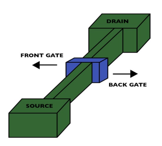
Figure 1.
Structure of FinFET.
The device’s effective width is provided by
where is fin thickness and is fin height.
By aligning the fins parallel, the width of a FinFET can be expanded. The effective channel width is determined by
If n numbers of identical fins are connected in parallel
Lg is the length of the gate covering the fin, and Lfinext is the length of the fin on two sides linking the source and drain as shown in Figure 1. FinFET is the ideal substitute for CMOS for eliminating the disadvantage of SCE and improving circuit performance at reduced technology nodes [7,8,9]. Although it is a more effective device than a CMOS transistor, it still has problems with leakage current, variability effect, and reliability effect, all of which affect the device’s performance metrics. Due to various SCEs that result in PVT changes, the FinFET transistor’s performance in the ultra-DSM regime is not entirely flawless. Any digital circuit design in the VLSI industry must satisfy the requirements during the fabrication process. Any digital circuit design’s potential performance is largely dependent on the fabrication method. As a result, during the manufacturing process, safety measures must be taken. However, creating digital circuits is a difficult process and any arbitrary adjustments will change how well the circuit works. Circuit performance changes can be caused by any of the circuit’s factors, including operational temperature and power supply voltage. These fluctuations could result in significant yield loss and affect how much a unit of the product costs if they go above the allowed ranges. Since these statistical fluctuations are inevitable, it is crucial to recognize them during the manufacturing process and incorporate the necessary steps into the circuit design [10]. Important precautions must be made during the manufacturing process to reduce the sensitivity of circuits to these differences. Moreover, safety measures should be taken for a significant number of manufactured circuits. These are the circumstances that support design for manufacture (DFM), Early in the design process, DFM is primarily focused on making items as cheaply and easily as possible. The evaluation of different concerns, including variability minimization, parametric yield maximization, parametric yield estimation, and worst-case analysis, is a key function of DFM in digital signal circuits, as well. The relationship between device parameters and processing, as well as how they affect system and circuit performance, is shown in Figure 1 In the DSM regime, metal oxide semiconductor (MOS) technology deposits oxide layers and photoresists using more than 30 masks and 200 chemical processes. All fabrication steps are controlled by the computer during the manufacturing process, which is extremely precise. Even with the utmost accuracy, mistakes in mask alignment, thickness management of thin gate oxide layers, chemical etching of poly-silicon gate length of MOS, and doping of contaminants are inevitable. Process differences affect how well digital circuits work, and their effects are seen in the circuits’ output waveforms. A particular transistor on a chip may have a drastically different drain current from its counterpart on a separate chip on the same wafer. This discrepancy may be noticeably bigger for chips on various wafers. We observe similarities between the parasitic capacitances and resistances in interconnection structures. Figure 1 illustrates how process variables can alter the output waveform of circuits. Random changes in drain current are the cause of any random fluctuations in circuit performance characteristics including logic threshold voltage, power consumption, and delay time. The sole designable parameter that the designer influences is the notional value of the aspect ratio. Therefore, the most obvious solution to reduce the susceptibility of circuit performance to process fluctuations is to select the ideal value of L and W for CMOS devices. Except for certain circuits, the majority of digital circuits use the minimum value of L. Complex circuits with level shifters and memory cells. Channel leakage is the fundamental constraint in these circuits. In order to decrease power dissipation and delay at 7 nm, simulations of FinFET domino circuits are done as per dimensions shown in Table 1. SRLC and HSCC proposed circuit shown low power dissipation and delay compared to existing, CMFD, HSCD, and MHSCD with the variation of temperature and supply voltage. The structure of this essay is as follows: Section 2 discusses several process modifications. Additionally, it includes a summary of earlier research on variability. In Section 3, various aspects of PVT simulations are covered. The concept of Monte Carlo simulation in the Cadence Virtuoso tool is also presented in this section. Following PVT simulations on several domino FinFET circuits, Section 4 presents the various logic domino styles. Results and discussions are presented in Section 5. The conclusion is found in Section 6.

Table 1.
FinFET Dimensions.
2. Prior Employment
In the VLSI sector, PVT variations are a highly important problem that affects parametric yield. Voltage fluctuations, environmental changes, and variations integrated into FinFET devices during lithography doping result in unexpected behavior in device performance and lower yield. Numerous researchers have addressed the issue of PVT changes in recent years and have proposed various PVT mitigation strategies. The numerous kinds of variations are shown in Figure 2. PVT variations are a significant scaling issue for FinFET technology. Variations can be broadly divided into two categories: (1) variations in the environment; and (2) variations in the process. Variations in supply voltage and temperature take environmental fluctuation into account. Process variations are the principal cause of random fluctuations. These switching activity variations cause temperature changes. Variations in switching activity throughout the semiconductor cause temperature changes. A voltage drop in a power grid causes supply voltage volatility. There are two further categories for process variations: systematic and non-systematic. Electrical parameters of transistors with the same width and length change in regular fluctuations. An in-depth analysis of the layout while the product is being manufactured can be used to correct these kinds of variations [11]. Non-systematic fluctuations are parts of process variations that were not anticipated. Although the cause of these variances is unknown, they happen during the production process. Two further non-systematic variants are inter-die and intra-die variances. Technical limitations and other factors lead to inter-die differences. Additional subcategories of intra-die variations include random and linked variations. It is considered that every other component of variation is statistically unrelated to random variation. Random variation is brought on by gate line edge roughness and random dopant fluctuation. Digital circuits in the VLSI sector depend heavily on memory, and using FinFET in memories significantly reduces power consumption. PVT changes can lead to several problems with a static random-access memory (SRAM), including data instability, low read current, and area overhead [12]. Work function fluctuations in the context of PVT variations enhance OFF-state leakage current. Different FinFET circuits will function differently as a result [13]. Gate length, fin height, and fin thickness are just a few of the FinFET device factors that affect how well a circuit performs. Any changes to the transistor’s geometrical and electrical properties will cause a delay in operation. Researchers looked at how variances were affected by various transistor architectures. Distinct transistor arrangements result in different PVT fluctuation behavior. Series transistors should be positioned far from the output node in FinFET circuits. The findings of several sizing procedures reviewed by researchers demonstrate the various effects of PVT fluctuations on various transistor configurations [14,15]. A designer has created a 4:2 compressor that is more energy-efficient, uses fewer transistors, and is smaller in size. Compared to earlier models, this compressor uses less energy and is smaller. FinFETs have developed into excellent transistors to replace MOSFETs due to their increased scalability, effectiveness, and control of SCEs. Any changes to the transistor’s geometrical and electrical properties will cause a delay in operation. FinFETs have developed into a perfect transistor to replace conventional CMOS transistors, according to research. PVT fluctuations in FinFET integrated circuits are caused by lithography, manufacturing, and environmental constraints on FinFETs. FinFET circuits experience delay and leakage as a result of these fluctuations. McPAT-PVT is a thorough framework examining changes in PVT, power, and latency in FinFET devices [16]. Due to the development of a transistor with a smaller size, a set of useful layout design principles have been added [17]. Research compares the parasitic element of 7 nm FinFET to 28 nm planar CMOS and shows how these differences influence it because of the FinFET’s three dimensional structure and additional layers. FinFET devices do, however, have inherent scaling issues that need to be resolved to advance VLSI technology.
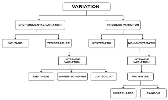
Figure 2.
Different kinds of variations.
3. PVT Simulation
As shown in Figure 3 and Figure 4, the main factors that cause PVT changes in VLSI devices include irregular working environment conditions, faulty fabrication processes, and irregular biasing. PVT changes primarily have an impact on the logic characteristics and performance parameters of logic gates and cause numerous fluctuations in the physical properties of FinFET devices. Therefore, in the deep nanoscale domain, it is necessary to assess each new, creative leakage reduction technique’s ability to tolerate variability and to introduce approaches that lessen the impact of variability. The unpredictable behavior of power factors and driving capabilities that FinFET transistors experience might cause each circuit to behave differently, resulting in anomalous power consumption and performance variance.
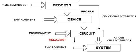
Figure 3.
Relationship between system performance, device specifications, and processing.
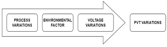
Figure 4.
PVT changes in FinFET devices.
4. Logic Domino Styles
Circuits of domino are favored over other dynamic logic types for the implementation of low power and delay CPU because they require less space and a lower level of precision (LP). Compared to dynamic CMOS, the pull-up network (PUN) of a (PMOS) transistor reduces both area and power consumption. In domino-style circuits, logic is implemented by an equal number of PMOSPMOS and NMOSNMOS transistors at the pull-up and pull-down of the network that is equal to the number of inputs given to the logic of the circuit with an inverter connect at the output. Short channel effects are also significant problems in circuit design for dominos [18]. In earlier articles, many methods for reducing leakage power and delay were proposed. Footless domino logic (FLDL) as shown in Figure 5 was the first method for domino logic architecture that was suggested [19]. With this method, the PMOS P1 gives a value VDD at the output when the clock is low. When the clock is high during the evaluation phase, the inputs are applied, and the pull-down network’s output changes following the applied input (PDN). When the charge held at the output in pre-charge mode is shared between the junction capacitance of transistors during the evaluation phase, a charge sharing problem arises [20,21]. The pre-charge transistor is connected in parallel with a keeper transistor whose gate is driven by output. Due to charge sharing and other factors, this keeper transistor prevents any unintended leakages and increases the circuit’s robustness. The fundamental drawback of this circuit is that subthreshold and gate tunnelling currents cause leakage currents to pass through the PDN during the evaluation phase when all inputs are low. The circuit becomes more resilient with the inclusion of keeper transistor P2, but propagation latency increases. The PMOSPMOS p2 stops the output node from unintentional leakage of charges. The output drops at the output node at a high voltage, which activates the PMOSPMOS keeper and maintains the high voltage. When the evaluation phase first begins, the keeper transistor prevents the dynamic from being discharged inadvertently. As a result, during the assessment phase, the NMOS logic circuit and PMOS p2 compete to check the output node’s ultimate state [22]. Contention between the keeper and PDN grows as the keeper’s size grows, increasing the circuit’s power and latency. As a result, smaller keepers are employed for speedier applications, whereas larger keepers are used for more durable designs. K = Wkeep/Weval, which yields the keeper ratio of [4,23]. As a result, increasing K results in increased robustness at the expense of increased power consumption and propagation delay. As depicted in Figure 6, to obtain footed domino logic and reduce off currents, FinFET NMOS is connected between the NMOS logic circuit and negative supply voltage [18,24,25]. The biggest drawback of this method is that speed drops when the footer transistor adds delay to the circuit. A current mirror-footed domino logic technique using transistor N2 to generate a stacking effect is displayed in Figure 7. N2 NMOS, however, will cause the circuit’s delay to grow throughout the evaluation phase. To reduce circuit latency, a current mirror circuit (N2-N3) is introduced. A current mirror transistor N3 is added in parallel, which causes the discharging current to increase to lessen this delay. Transistor N4 establishes a feedback link from the current mirror’s gate to the circuit’s output to halt the dynamic node’s discharge. Transistor N4 connects the gate of mirror transistors to earth when the dynamic node discharges to the ground as a result of noise at the input. The stacked transistors N1, N2, and transistors in evaluation mode decrease voltage when the clock is high and all of the inputs are at logic low. The main drawback of this circuit is the additional N2, N3, and N4 transistors’ increased area and power consumption. Transistor N1 is on in the high-speed clocked delay (HSCD) circuit as seen in Figure 8. Two inverters’ worth of delay later, transistor N1 goes off. As a result, the voltage at node N rises. Output node N is connected to negative supply voltage which makes node N and N2 logic 0. Transistor sizing and clock input1 are given in such a way that the Vth of NMOS N2 is higher than node N voltage which makes NMOS N2 off for the clock input 0. The stacked transistor N2 enhances noise immunity in this manner. Due to the circuit having more transistors than FLDL and FDL, its biggest drawback is space. As a result, node N is linked and gives forward bias voltage to the transistor for clock input of logic 1 for minimizing off-current power usage. By expanding the size of the N1, N2, or evaluation transistors, the speed of the logic can be enhanced. Figure 9 illustrates a logic and gate, and NMOS transistor MD is added to the HSCD approach to speed up the logic for clock input of logic 1 to obtain Modified HSCD. The high impedance of N2 input during the pre-charge phase results from more consumption of power. In addition, power usage in the pre-charge mode is increased by the floating gate of N2. The MHSCD technique’s floating gate problem has been overcome in the circuit. Two N-channel transistors N2 and N3 are stacked in this circuit between the dynamic node and ground, as depicted in Figure 9. A significant issue with the circuit is that the gate of transistor N2 is in a high impedance state during the pre-charge phase, which causes the two transistors to turn on in response to the footer transistor N1′s on/off status. This method is known as domino logic conditional evaluation (CEDL). The breadth of the evaluation of the domino circuit determines its latency. The width of the transistor grows, and the circuit’s latency also increases. The simulation of proposed SRLC circuit is shown in Figure 10.
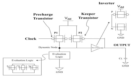
Figure 5.
Domino logic without foot (DLWF) [26].
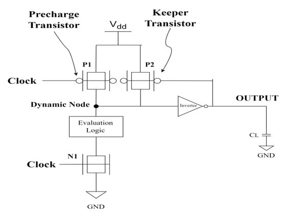
Figure 6.
Logical dominos with foot (LDF) [26].
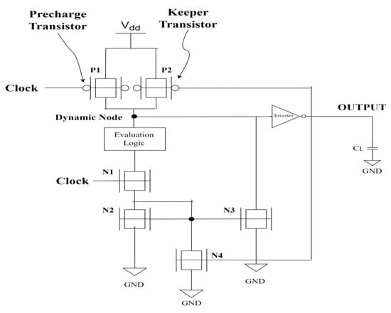
Figure 7.
Current mirror-footed domino (CMFD) [26].
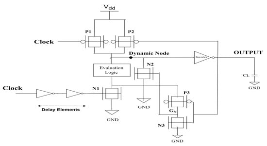
Figure 8.
High-speed clocked delay (HSCD) [26].
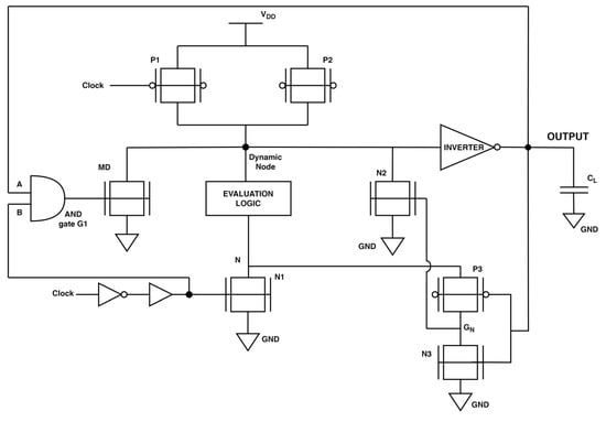
Figure 9.
Modified high-speed clocked delay (MHSCD) [26].
Figure 10.
Transient waveforms of a two-input OR gate implemented using the proposed SRLC technique in FinFET technologyat a clock frequency of 100 MHz.
4.1. Set Reset Logic Circuit (SRLC)
CMOS dynamic logic has many drawbacks in addition to its advantages of great performance and speed. CMOS dynamic logic circuits perform poorly due to issues like charge leakage, charge sharing, loss of noise immunity, and timing issues. To solve these issues, circuits with self-resetting logic have been developed as shown in Figure 11 and Figure 12. Asynchronous working is supported by a self-resetting logic circuit. For low-power and high-speed applications, set-reset logic circuits are used as shown in Table 2 SRLC circuits are used in high-performance data communication and network systems. For the inclusion of cascaded inverters placed between the output and input of PMOS gate, it should be noted that the feedback uses an odd number of inverters: three. The feedback loop significantly affects the functioning of the circuit. When the clock reaches a certain value, pre-charging takes place. Inputs to all logic NMOS remain zero during pre-charge for the elimination of leakage which makes MR gate voltage have logic 1.MR gate voltage gets 0 volts from the cascaded inverters and automatically makes the output to logic 1. This helps with “current spike” issues in big chips. The source-gate voltage that is delivered to MR during the pre-charge pushes it towards cutoff. The outcomes of a discharge event that is triggered by the evaluation’s input variables for the condition xy = 1 is described by a pulse whose duration is set by the driving circuit, presuming that the inputs x and y are obtained via a self-resetting circuit. This enables the transition by allowing discharge to the earth. The output voltage increases to a value and is applied across the inverter chain to raise the MR’s source-gate voltage. Source-gate following a delay of the voltage of MR flips to a value that MR is a closed loop. The output is pulsed as it is depicted because the reset transistor charges back up to a voltage that causes the transition. The updated output voltage is supplied to the inverter chain, which causes MR to be turned off. This demonstrates how MR is set up in feedback to automatically recharge the internal node, which resets the output to zero. A self-resetting gate’s output voltage is a voltage pulse whose width is governed by circuit delays. Because it is sensitive to delay times, self-resetting logic can be trickier to utilize. It does, however, allow for some fascinating circuit design alternatives. Self-resetting circuits, for instance, can be utilized for asynchronous logic. Also, unlike in typical dynamic logic, the power supply current utilized to pre-charge is dispersed across time rather than being focused during a single period of the pre-charge cycle. This helps with “current spike” issues in big chips. It is feasible to compare a self-resetting logic chain to a domino effect.
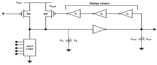
Figure 11.
A self-resetting logic circuit (SRLC).
Figure 12.
A self-resetting logic circuit (SLRC) with domino-footed logic.
Table 2.
Comparison of parameters for various domino logic circuits of temperature value 10 °C.
4.2. High-Speed Cascade Circuit (HSCC)
A domino logic chain’s speed is constrained by the gate discharge time. An ordinary domino circuit makes up the first stage. However, the second stage has undergone two changes: the NMOS has been eliminated, and the pre-charge pFET’s clock signal has been switched to a delayed clock signal. Table 3 shown the comparison of proposed HSCC circuit with existing domino logic circuits. A high-speed cascade circuit is shown in Figure 13. This kind of configuration produces a cascade that is error-free and has an enhanced second stage. The non-inverting buffer, which is made up of two cascaded inverters, is crucial to understanding the operation. Before being applied to the second stage, the high-speed domino circuit is delayed by a certain amount. A clock value causes the internal node to be pre-charged, which takes time tch = tpsp. This causes the output voltage Vout to drop to 0 volts after the inverter’s time tLH.The second stage’s logic FET M2 is ensured to be in cutoff by a high-speed domino circuit. This breaks the connection between the Cx2 of the delayed stage and negative supply voltage at time t and zero. By the time the delayed clock transitions to M2, M2 has already turned off, directing all of the pre-charge current IDD through the clocking pFET MpD to Cx2. This guarantees that the circuit will function properly during the (delayed) evaluation. The right clock delay is the key consideration in the design of this kind of cascade. The length of the value must be sufficient to ensure that the first stage’s output has gone below the nFET in the next logic chain’s threshold voltage. For single-stage domino circuits, discharge gate time is the limitation. To decrease delay, therefore, cascade stage is implemented as shown in Figure 13. The proper delay between clocks is determined by the cascade stage as shown in Figure 14. When a glitch is introduced, the process variations do not increase the delay as temperature increases. Due to fewer capacitance currents in HSCC, power is reduced as compared to SRLC as governed by
dynamic power dissipation
C capacitance
supply voltage
F clock frequency

Figure 13.
High-speed cascade circuit.

Figure 14.
Timing requirement high-speed cascade circuit.
Table 3.
Comparison of various types of domino logic circuits.
Table 3.
Comparison of various types of domino logic circuits.
| S. No | Domino Logic | Differences in Various Domino Logic |
|---|---|---|
| 1. | Footless domino logic | Advantage: High-speed compared to dynamic logic. Disadvantage: In footless domino logic, charge sharing takes place at junctions of the transistor and output capacitance. |
| 2. | Footed domino logic circuits | Advantage: It reduces off current with the connection ofNMOSbetween the logic circuit and ground.Disadvantage: Drops the speed due to high delay in the circuit |
| 3. | CMFD (Current mirror footed Domino) | Advantage: In CMFD NMOStransistors N2 and N3 are included in the footed domino logic to increase speed, and N4 is added to increase noise margin. Disadvantage: Addition of NMOS transistor N2,N3,N4 increase area andpower consumption. |
| 4. | HSCD (High-speed clocked delay) | Advantage: The stacked transistor N2 enhances noise immunity. Disadvantage: Due to the circuit having more transistors than FLDL and FDL, its biggest drawback is space |
| 5. | Set and reset logic circuit (SRLC) | Existing CMOS domino logic circuits perform poorly due to issues like charge leakage, charge sharing, loss of noise immunity, and timing issues. To solve these issues, circuits with self-resetting logic have been developed which have low power and high speed compared to existing ones. Disadvantage: used only for an asynchronous circuit |
| 6. | High speed cascade circuit (HSCC) | Advantage: The existing domino logic circuits have the limitation of gate discharge time which reduces the speed and increases the power of domino with the single stage which is overcome by the cascade stage. |
5. Results and Discussions
The power dissipation of any circuit has been determined for variable voltage to obtain the optimal operational parameters for the circuit. The voltage has been varied from 0.7 to 1.2 V. The dynamic power consumption of any circuit is directly proportional to the operational frequency and square of the voltage as explained in Equation (4). With an increase in the operating voltage and frequency, there is an increase in power dissipation. As per the equation mentioned below, the number of switching bits (NSW) determines the clock speed which is directly proportional to the clock frequency.
The dynamic power dissipation is given by
Cpd → power consumption capacitance
F1 → input frequency
F → output frequency
NSW → total no of switching bits
→ load capacitance
Vcc → supply voltage
The power dissipation of any circuit depends on the logic, technology node, implementation style, frequency of operation, and voltage. The most direct strategy to lower the power consumption of any circuit is to use a new technological process and operate near-threshold voltage. The circuit uses a FinFET with a length of the channel of 7 nm. Due to the smaller dimensions in the nm range, there is a reduction in leakage current, lowering power dissipation as explained in Equation (6).
where N is the number of transistors, Vdd is the supply voltage, I is the leakage current, and Kdesign is an empirical factor oriented with the sizing of the transistors and design style. According to the scaling theory, when a circuit is ported to the next technology generation, it is expected to operate at a reduced supply voltage which, in turn, reduces the power consumption. The transistor works by adjusting the electric field across the silicon substrate under the gate to control the current flow between the drain and the source [27]. Scaling down of physical dimensions of the device modifies the doping levels and voltage by a factor α [26,28]. The transconductance remains the same throughout the scaling process whereas the capacitance decreases by a factor α. This leads to a reduction in power dissipation by α 2 times due to the reduced voltage and current. The propagation delay is studied by varying the technology node, and operating voltage for the fixed technology node for FinFET. The propagation delay of the circuit depends on the clock speed, voltage of operation and other parameters. The clock speed of the circuit is inversely proportional to the frequency of operation. The propagation delay is inversely proportional to the voltage as mentioned in Equation (7).
The propagation delay Tp depends on capacitance C, width-to-length ratio W/L of the FinFET, and the operational voltage VDD. Keeping the other parameters constant and varying the voltage, the delay increases with a decrease in voltage and vice versa as it is inversely proportional to VDD. In this research, the performance of power dissipation and delay with respect to fluctuation of temperature and supply voltage is studied using high performance FinFET based circuits at 7 nm, where the parameters of the FinFET are taken as indicated in Table 1. The idea behind the technology of the proposed FinFET SRLC and HSCC domino logic circuit is the improvement of power dissipation, delay as depicted in Table 3 and area reduction as compared to the existing domino logic style as shown in Table 2. The suggested circuit SRLC and HSCC with FinFET technology offer a maximum power reduction compared to the CMFD, HSCD, MHSCD, and existing domino logic circuits shown in Table 4. When compared to the CMFD technique, the suggested technique offers a maximum delay reduction. The suggested 7 nm FinFET-based circuits demonstrate a maximum power reduction compared to its equivalent in FinFET technology circuits with the variation of temperature as shown in Table 5 and voltage. The suggested circuits are ensured with Monte-Carlo analysis as shown in Table 6. As temperature increases, the mobility of charge carriers decreases which increases the thermal equivalent voltage and leakage currents, thus resulting in high power dissipation as shown in Figure 15. The leakage current is given by
where Vth represents threshold voltage, W/L is the ratio of channel width to the effective channel length, Cox denotes gate oxide capacitance per unit width, μ0 indicates zero bias mobility, VT represents thermal equivalent voltage, m depicts sub-threshold swing coefficient, VDS is the drain to source voltage, and η is drain-induced barrier-lowering coefficient. As temperature increases, the threshold voltage decreases which can lead to an increase in leakage currents, thus increasing delay Figure 16 and power dissipation. In circuits, power dissipation consists of two parts: a dynamic part and a static (leakage) part. The dynamic power dissipation [29] is given below:
where α is the activity factor, C is the switching capacitance, and f is the clock frequency. Hence, in the simulation results of Figure 15, as temperature increases, power dissipation increases due to an increase in leakage currents and switching capacitance. In Figure 16, as temperature increases, delay increases due to the increase of Vt and decrease of Ion on the current in FinFET as related by Equation (10) and Equation (11). When operating under the super-threshold, the operation environment changes to Vth can have a direct impact on the Ion of FinFET. Ion(T) [30], often a function of temperature T, can be written as follows:
where β is the velocity saturation effect factor, S is the subthreshold swing, and Vgs is the gate-source voltage. In FinFET domain circuits, the increase in supply voltage can lead to an increase in power dissipation due to an increase of threshold voltage and leakage current [31] as shown in Figure 17. This leads to a decrease in the on-current and an increase in off-current resulting in an increase in power dissipation. The higher supply voltage can cause an increase in leakage currents, especially when the transistors are in the off state as given by Equation (8). The higher supply voltage can further increase the switching speed of the transistors, leading to an increasingly dynamic power dissipation as given by Equation (9). In FinFET-based domain circuits, the decrease in supply voltage can lead to an increase in delay due to reduced current with decreasing supplying voltage as shown in Figure 18. This results in slower switching times, which can lead to increased delay. FinFET circuits have higher parasitic capacitance compared to traditional planar CMOS circuits due to the three-dimensional nature of the FinFET structure. The supply voltage reducing the charging and discharging of this capacitance leads to increased delay. FinFET circuits operate at higher frequencies than traditional planar CMOS circuits which can result in increased dynamic power dissipation; however, reducing the supply voltage can reduce the power consumption which, in turn, reduces the dynamic power dissipation that leads to slower switching times and increased delay. Figure 19 shows comparison of power dissipation with rise of temperature for proposed SRLC with existing one. To overcome the problem of the rise of temperature resulting in high delay, simulation is carried out for the SRLC circuit at reduced supply voltage from 0.7 V to 0.2 V and temperature 0 °C to 100 °C, using bulk FinFET in BSIMCMG FinFET at 7 nm which is not carried out in previous work. Scaled technologies have investigated the massive, temperature-dependent rise in leakage current caused by band gap narrowing and thermal generation in the channel in modern integrated circuits [29,30]. The bulk FinFET is modelled using BSIM-CMG, a surface potential-based industry-standard model for domino logic circuits [31]. The simulation results in Figure 20 show that FinFET, in bulk and due to the dominance of Vth reduction for highly scaled devices at reduced supply voltages resulting from the stress-induced bandgap narrowing effect, the ON-state current rises with temperature. Due to the dielectric layer’s expansion as a function of temperature, the tall and narrow fins are stressed [32]. The stress effect makes the bandgap narrowing effect more potent as the effective fin aspect ratio rises, leading to a greater ON state. Due to a comparable drop in threshold voltage (Vth), FinFETs experience an ON-state current increase as the temperature rises [33]. Hence, RON (on resistance) also drops by the same amount, which reduces delay. At all supply voltage levels, FinFETs operate more quickly as the temperature rises [33]. The simulation results in Figure 21 show that Fine in bulk, due to the dominance of Vth reduction for highly scaled devices at reduced supply voltages, decreases delay, a finding which is not shown in any earlier work.
Table 4.
Comparison of various FinFET domino logic styles at 7 nm technology node.
Table 5.
Comparison of power dissipation of various proposed FinFET domino logic styles with existing one at 7 nm technology node for the rise of the temperature value.
Table 6.
Monte Carlo simulation values.
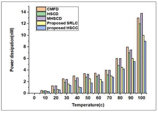
Figure 15.
Simulation of power dissipation with the temperature of FinFET-based circuits at 7 nm.
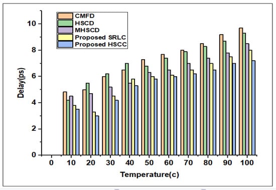
Figure 16.
Simulation of delay with the temperature of FinFET-based circuits at 7 nm.
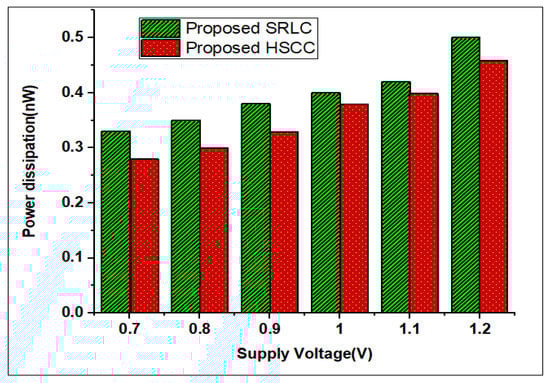
Figure 17.
Simulation of power dissipation with a supply voltage of FinFET-based circuits at 7 nm.
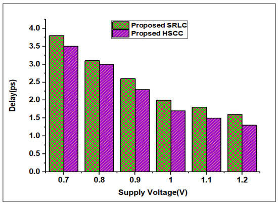
Figure 18.
Simulation of delay with a supply voltage of FinFET-based circuits at 7 nm.
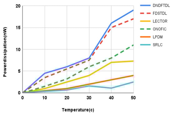
Figure 19.
Simulation of power dissipation with varied temperatures of FinFET based SRLC circuit at 7 nm. The abbreviations used in the above table are as follows. CMFD: Current mirror footed logic. HSCD: High speed clocked delay. MHSCD: Modified high speed clocked delay. SRLC: Set and reset logic circuit (proposed). HSCC: High speed cascade circuit. LECTOR: Leakage control transistor technique. ONOFIC: ON/OFF logic. DNDFTDL: Dynamic node-driven feedback transistor domino logic. FDSTDL: Foot-driven stack transistor domino logic. LPDT: Low-power domino technique.
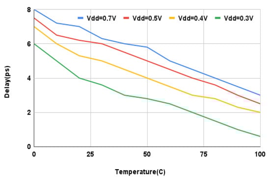
Figure 20.
Simulation of delay with the variation of temperatures at different Vdd of FinFET-based SRLC circuit at 7 nm.
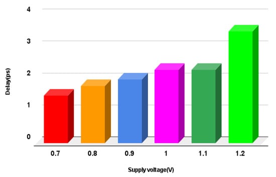
Figure 21.
Simulation of delay with the variation of supply voltage at Vt =0.02 V of FinFET-based SRLC circuit at 7 nm.
Mean and standard deviation are the Monte Carlo analysis techniques used to enable the research and forecasting of fluctuations in circuit performance that have an impact on yield as shown in Table 6. In this analysis of statistics, blocks are used that contain correlations and statistical distributions of circuit netlist parameters. For board-level designs, netlist also represents components or process modifications used in the manufacture of integrated circuits.
6. Conclusions
This paper proposes a new performance analysis for various domino logic circuits with the variation of temperature and voltage at a 7 nm technology node. The suggested domino logic circuits show that an increase in temperature and voltage increases power and delay. In FinFET technology, simulation results show that the proposed circuit reduces power by 50% when compared to the existing CMFD and MHSCD techniques, and a 60%reduction of delay when compared to the CMFD and MHSCD techniques. In comparison to the existing low-power domino method technique, the proposed technique SRLC showed a 25% delay reduction for the rise of temperature at a reduced supply voltage value of 0.3 Vin comparison to existing CMFD and HSCD techniques in FinFET mode, the proposed SRLC circuit improves in area reduction. In comparison to the existing low-power domino method technique, the proposed technique SRLC showed a 60% delay reduction at reduced supply voltage and threshold voltage. When compared to other existing circuits, Monte Carlo analysis ensures the robustness of the proposed circuit. In comparison to existing techniques, the proposed technique has lower power consumption, less propagation delay, and low area.
Author Contributions
Conceptualization, K.B.; methodology, K.B.; software, A.N.; validation, K.B.; formal analysis, A.N.; investigation, A.N.; data curation, A.N.; writing—original draft preparation, A.N.; writing—review and editing, A.N.; visualization, K.B.; supervision, K.B.; project administration, K.B. All authors have read and agreed to the published version of the manuscript.
Funding
This research received no external funding.
Conflicts of Interest
The authors declare that they have no known competing interest or personal relationship that could have appeared to influence the work reported in this paper.
References
- Sharma; Sharma, V.K. An efficient low power method for FinFET domino OR logic circuit. Microprocess. Microsyst. 2022, 95, 104719. [Google Scholar] [CrossRef]
- Sreenivasulu, V.B.; Narendar, V. Performance improvement of spacer engineered n-type SOI FinFET at 3-nm gate length. AEU-Int. J. Electron. Commun. 2021, 137, 153803. [Google Scholar] [CrossRef]
- Magraiya, V.K.; Gupta, T.K. ONOFIC-based leakage reduction technique for FinFET domino circuits. Int. J. Circuit Theory Appl. 2018, 47, 217–237. [Google Scholar] [CrossRef]
- Razavieh, A.; Zeitzoff, P.; Nowak, E.J. Challenges and Limitations of CMOS Scaling for FinFET and Beyond Architectures. IEEE Trans. Nanotechnol. 2019, 18, 999–1004. [Google Scholar] [CrossRef]
- Magraiya, V.K.; Gupta, T.K. ONOFIC pull-up approach in domino logic circuits using FinFET for subthreshold leakage reduction. Circuits Syst. Signal Process. 2019, 38, 2564–2587. [Google Scholar] [CrossRef]
- Sreenivasulu, V.B.; Narendar, V. A Comprehensive Analysis of Junctionless Tri-Gate (TG) FinFET Towards Low-Power and High-Frequency Applications at 5-nm Gate Length. Silicon 2021, 14, 2009–2021. [Google Scholar] [CrossRef]
- Kumar, T.S.; Tripathi, S.L. Leakage Reduction in 18 nm FinFET based 7T SRAM Cell using Self Controllable Voltage Level Technique. Wirel. Pers. Commun. 2020, 116, 1837–1847. [Google Scholar] [CrossRef]
- Sreenivasulu, B.V.; Vadthiya, N. Design and Deep Insights into Sub-10 nm Spacer Engineered Junctionless FinFET for Nanoscale Applications. ECS J. Solid State Sci. Technol. 2021, 10, 013008. [Google Scholar]
- Bagheriye, L.; Toofan, S.; Saeidi, R.; Moradi, F. Highly stable, low power FinFET SRAM cells with exploiting dynamic back-gate biasing. Integration 2018, 65, 128–137. [Google Scholar] [CrossRef]
- Sharma, V.K.; Pattanaik, M.; Raj, B. INDEP approach for leakage reduction in nanoscale CMOS circuits. Int. J. Electron. 2014, 102, 200–215. [Google Scholar] [CrossRef]
- Sharma, V.K.; Pattanaik, M. Design of low leakage variability-aware ONOFIC CMOS standard cell library. J. Circuits Syst. Comput. 2016, 25, 1650134. [Google Scholar] [CrossRef]
- Alioto, M.; Palumbo, G. Impact of supply voltage variations on full adder delay: Analysis and comparison. IEEE Trans. Very Large Scale Integr. (VLSI) Syst. 2006, 14, 1322–1335. [Google Scholar] [CrossRef]
- Kajal, S.V.K. FinFET: A Beginning of Non-Planar Transistor Era. In Nanoscale VLSI: Devices Circuits Applications; Springer: Singapore, 2020; pp. 139–159. [Google Scholar]
- Sharma, V.K.; Pattanaik, M. Process, voltage and temperature variations aware low leakage approach for nanoscale CMOS circuits. J. Low Power Electron. 2014, 10, 45–52. [Google Scholar] [CrossRef]
- Zimpeck, A.; Meinhardt, C.; Reis, R. Impact of PVT variability on 20 nm FinFET standard cells. Microelectron. Reliab. 2015, 55, 1379–1383. [Google Scholar] [CrossRef]
- Zimpeck, A.; Meinhardt, C.; Artola, L.; Hubert, G.; Kastensmidt, F.; Reis, R.A.D.L. Impact of different transistor arrangements on gate variability. Microelectron. Reliab. 2018, 88, 111–115. [Google Scholar] [CrossRef]
- Zimpeck, A.L.; Meinhardt, C.; Posser, G.; Reis, R. FinFET cells with different transistor sizing techniques against PVT variations. In Proceedings of the 2016 IEEE International Symposium on Circuits and Systems (ISCAS), Montreal, QC, Canada, 22–25 May 2016. [Google Scholar]
- Tang, A.; Yang, Y.; Lee, C.-Y.; Jha, N.K. McPAT-PVT: Delay and power modelling framework for FinFET processor architectures under PVT variations. IEEE Trans. Very Large Scale Integr. (VLSI) Syst. 2014, 23, 1616–1627. [Google Scholar] [CrossRef]
- Ilin, S.; Ryzhova, D.; Korshunov, A. Comparative analysis of standard cells performance for 7 nm FinFET and 28 nm CMOS technologies with considering for parasitic elements. In Proceedings of the 2018 IEEE Conference of Russian Young Researchers in Electrical and Electronic Engineering (EIConRus), Moscow, St. Petersburg, Russia, 29 January–1 February 2018. [Google Scholar]
- Liao, K.; Cui, X.; Liao, N.; Ma, K.; Wu, D.; Wei, W.; Li, R.; Yu, D. Ultra-low power dissipation of improved complementary pass-transistor adiabatic logic circuits based on FinFETs. Sci. China Inf. Sci. 2014, 57, 1–13. [Google Scholar] [CrossRef]
- Mahmoodi-Meimand, H.; Roy, K. Diode-footed domino: A leakage-tolerant high fan-in dynamic circuit design style. IEEE Trans. Circuits Syst. I: Regul. Pap. 2004, 51, 495–503. [Google Scholar] [CrossRef]
- Cheng, C.H.; Chang, S.C.; Wang, J.S.; Jone, W.B. Charge sharing fault detection for CMOS domino logic circuits. In Proceedings of the 1999 IEEE International Symposium on Defect and Fault Tolerance in VLSI Systems (EFT’99), Albuquerque, NM, USA, 1–3 November 1999. [Google Scholar]
- Gupta, T.K.; Khare, K. Lector with footed-diode inverter: A technique for leakage reduction in domino circuits. Circuits Syst. Signal Process. 2013, 32, 2707–2722. [Google Scholar] [CrossRef]
- Wey, I.-C.; Chang, C.-W.; Liao, Y.-C.; Chou, H.-J. Noise-tolerant dynamic CMOS circuits design by using true single-phase clock latching technique. Int. J. Circuit Theory Appl. 2015, 43, 854–865. [Google Scholar] [CrossRef]
- Dadoria, A.; Khare, K.; Gupta, T.K.; Singh, R.P. A novel high-performance leakage-tolerant, wide fan-in domino logic circuit in deep-submicron technology. Circuits Syst. 2015, 6, 103–111. [Google Scholar] [CrossRef]
- Garg, S.; Gupta, T.K. Low power domino logic circuits in deep-submicron technology using CMOS. Eng. Sci. Technol. Int. J. 2018, 21, 625–638. [Google Scholar] [CrossRef]
- Gong, N.; Guo, B.; Lou, J.; Wang, J. Analysis and optimization of leakage current characteristics in sub-65 nm dual Vt footed domino circuits. Microelectron. J. 2008, 39, 1149–1155. [Google Scholar] [CrossRef]
- Moradi, F.; Peiravi, A.; Mahmoodi, H. A new leakage-tolerant design for high fan-in domino circuits. In Proceedings of the16th International Conference on Microelectronics, 2004, ICM 2004, Tunis, Tunisia, 6–8 December 2004. [Google Scholar]
- Gupta, A.; Mathur, R.; Nizamuddin, M. Design, simulation and comparative analysis of a novel FinFET based astable multivibrator. AEU-Int. J. Electron. Commun. 2019, 100, 163–171. [Google Scholar] [CrossRef]
- Lee, W.; Wang, Y.; Cui, T.; Nazarian, S.; Pedram, M. Dynamic thermal management for FinFET-based circuits exploiting the temperature effect inversion phenomenon. In Proceedings of the 2014 International Symposium on Low Power Electronics and Design, La Jolla, CA, USA, 11–13 August 2014. [Google Scholar]
- University of California, Berkeley. BSIM-CMG 110.0.0 Technical Manual; University of California, Berkeley: Berkeley, CA, USA, 2016. [Google Scholar]
- Kim, S.-Y.; Kim, Y.M.; Baek, K.-H.; Choi, B.-K.; Han, K.-R.; Park, K.-H.; Lee, J.-H. Temperature dependence of substrate and drain–currents in bulk FinFETs. IEEE Trans. Electron Devices 2007, 54, 1259–1264. [Google Scholar] [CrossRef]
- Saha, S.; Kumar, U.S.; Baghini, M.S.; Goel, M.; Rao, V.R. Impact of thermal effects on the performance of the power gating circuits using NEMS, FinFETs, and NWFETs. IEEE Trans. Electron Devices 2021, 68, 2618–2624. [Google Scholar] [CrossRef]
- Garg, S.; Gupta, T.K. FDSTDL: Low-power technique for FinFET domino circuits. Int. J. Circuit Theory Appl. 2019, 47, 917–940. [Google Scholar] [CrossRef]
Disclaimer/Publisher’s Note: The statements, opinions and data contained in all publications are solely those of the individual author(s) and contributor(s) and not of MDPI and/or the editor(s). MDPI and/or the editor(s) disclaim responsibility for any injury to people or property resulting from any ideas, methods, instructions or products referred to in the content. |
© 2023 by the authors. Licensee MDPI, Basel, Switzerland. This article is an open access article distributed under the terms and conditions of the Creative Commons Attribution (CC BY) license (https://creativecommons.org/licenses/by/4.0/).