Communication

A Filtering Antenna with Slots and Stacked Patch Based on SISL for 5G Communications

School of Microelectronics, Tianjin University, Tianjin 300072, China
*
Author to whom correspondence should be addressed.
Electronics 2023, 12(6), 1331; https://doi.org/10.3390/electronics12061331
Submission received: 10 February 2023 / Revised: 4 March 2023 / Accepted: 7 March 2023 / Published: 10 March 2023
(This article belongs to the Special Issue Substrate Integrated Circuits and Antennas)

Abstract

:
A filtering antenna based on the Substrate Integrated Suspended Line (SISL) platform applied for the n78 band of 5G is presented in this paper. The antenna has a segmented feed line, a rectangular driven patch etched with a double I-slot, and a squared stacked patch with grooves at the edges of both sides. The etched slots and the stacked patch introduce two new resonance frequencies increasing the bandwidth. Furthermore, the etched slots excite a deep radiation null in the low-frequency band, and the stacked patch coupled with the driven patch produces two deep radiation nulls in the high-frequency band. Three radiation nulls enable high selectivity of the antenna. The filtering antenna works at 3.2–3.89 GHz, which can be applied to the 5G (n78, 3.3–3.8 GHz) frequency band. The peak gain in the band can reach 9.21 dBi, and the out-of-band suppression levels are higher than 18.47 dB.

Graphical Abstract

1. Introduction

Wireless communication is in the era of the coexistence of 4G and 5G, and electromagnetic waves of different frequency bands are easy to interfere with one another. The filtering antenna is able to integrate the antenna and the filter, which can filter the interference signal while receiving and transmitting the electromagnetic wave signal and realize the miniaturization of the 5G communication system.
The traditional approach to design involves creating the filter and antenna separately and then connecting them in series to select the desired frequency band and filter out unwanted signals [1,2,3,4,5]. The filtering circuit or network can also be introduced into the antenna for collaborative design [6,7,8,9]. In [4], the filtering antenna is loaded with a first-order microstrip filter using an open-loop resonator and a third-order hairpin bandpass filter in the RF path to realize the filtering function of the antenna. However, these design methods often result in issues such as increased size, complex structure, added losses, and impedance mismatches in communication systems.
A method of shaping the microstrip patch antenna is proposed to improve these shortcomings. Common methods include etching slots [10,11,12,13,14,15], shorting pins [14,15,16,17,18], parasitic structure or stacked patches [15,17,19,20,21], shorting loops [22], etc. This design method does not require any filter or filtering circuit, which not only simplifies the circuit and solves the problem of insertion loss caused by introducing a filter, but also reduces the size of the antenna and facilitates the miniaturization of the system. For instance, in [11], a method of etching four slots on a single patch was employed to achieve multiple operating modes in the design of a filtering antenna. However, this design method uses a relatively large number of slots, which can easily disturb the current and field distribution on the patch, greatly affecting the resonance mode and increasing the design difficulty. In [14], the joint action of slots, strips, and shorting pins makes the antenna generate a filtering response, but it is relatively sensitive. In [20], the antenna is loaded with two layers of stacked patches of different sizes, and a radiation null appears at each edge of the frequency band to achieve filtering. However, this inevitably enlarges the profile and volume of the antenna. In [21], the antenna uses two coupling slots for feeding, forming multiple coupling paths. However, the slot-coupling may introduce certain radiation and scattering losses, which may increase the antenna’s loss. Therefore, the gain of the antenna is only 4.8 dBi. In [22], the radiation suppression level of the lower higher stopband is ameliorated by introducing a shorting loop and a pair of stubs. However, its complexity and profile are greatly increased. In the above filtering antenna design, some methods will increase the size and complexity of the antenna. Etched slots may have little effect on the patch. A combination of methods is usually used to achieve the required bandwidth and filtering response. In practical designs, not all antenna designs incorporating these structures can achieve filtering characteristics. For example, in [23], the antenna is loaded with stacked patches, etched slots, and pins, but its purpose is to enhance the pattern and obtain multiple operating bands. In [24], the designed antenna uses a crescent-shaped substrate, a rotated L-shaped monopole, and a DGS, but it does not obtain filtering characteristics.
It is worth mentioning that the most commonly used method for analyzing the filtering principle of a filtering antenna is to analyze the field distribution at the radiation nulls. For example, in [16,20,24], the filtering characteristics are explained by analyzing the cancellation of radiation through the electric field or current distribution at each radiation null.
Based on the SISL structure, a variety of filtering antennas that can be applied to different 5G frequency bands are proposed [25,26,27,28,29,30]. For example [26], the antenna uses low-cost FR4 material, which has the advantages of low cost and high gain. The antenna uses differential feeding, which can improve the performance of the antenna, but the use of two feeding ports makes the antenna design more complicated and requires high matching requirements. The SISL structure has the advantages of low loss, small size, lightweight, high integration, and self- packaged. The use of SISL structure can make the design of antenna structure more flexible and diverse. At the same time, low-cost dielectric materials can be used to reduce the antenna cost.
In this paper, a high gain, high selectivity, and coverage of n78 band SISL filtering antenna with etched slots and a stacked patch for 5G systems is proposed. The antenna uses the SISL structure as the design platform. The filtering performance is achieved through loading a stacked patch and two symmetrical I-slots on the edge of the rectangular driven patch. The I-slots can generate a radiation null at the low-frequency edge of the frequency band, and the stacked patch can engender two radiation nulls on the high-frequency side. The suppression level is higher than 18.47 dB.

2. Antenna Devise and Operating Principle
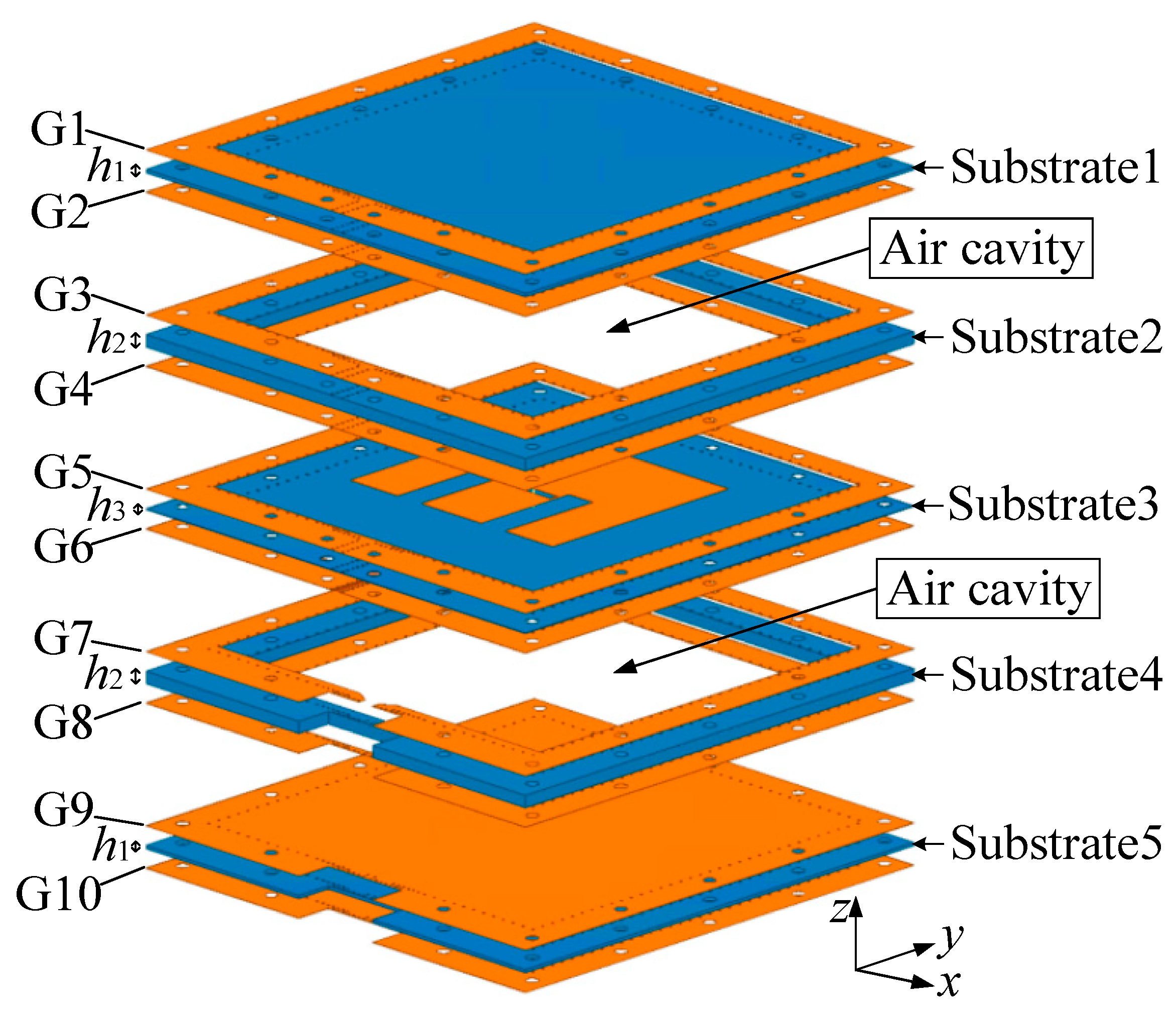
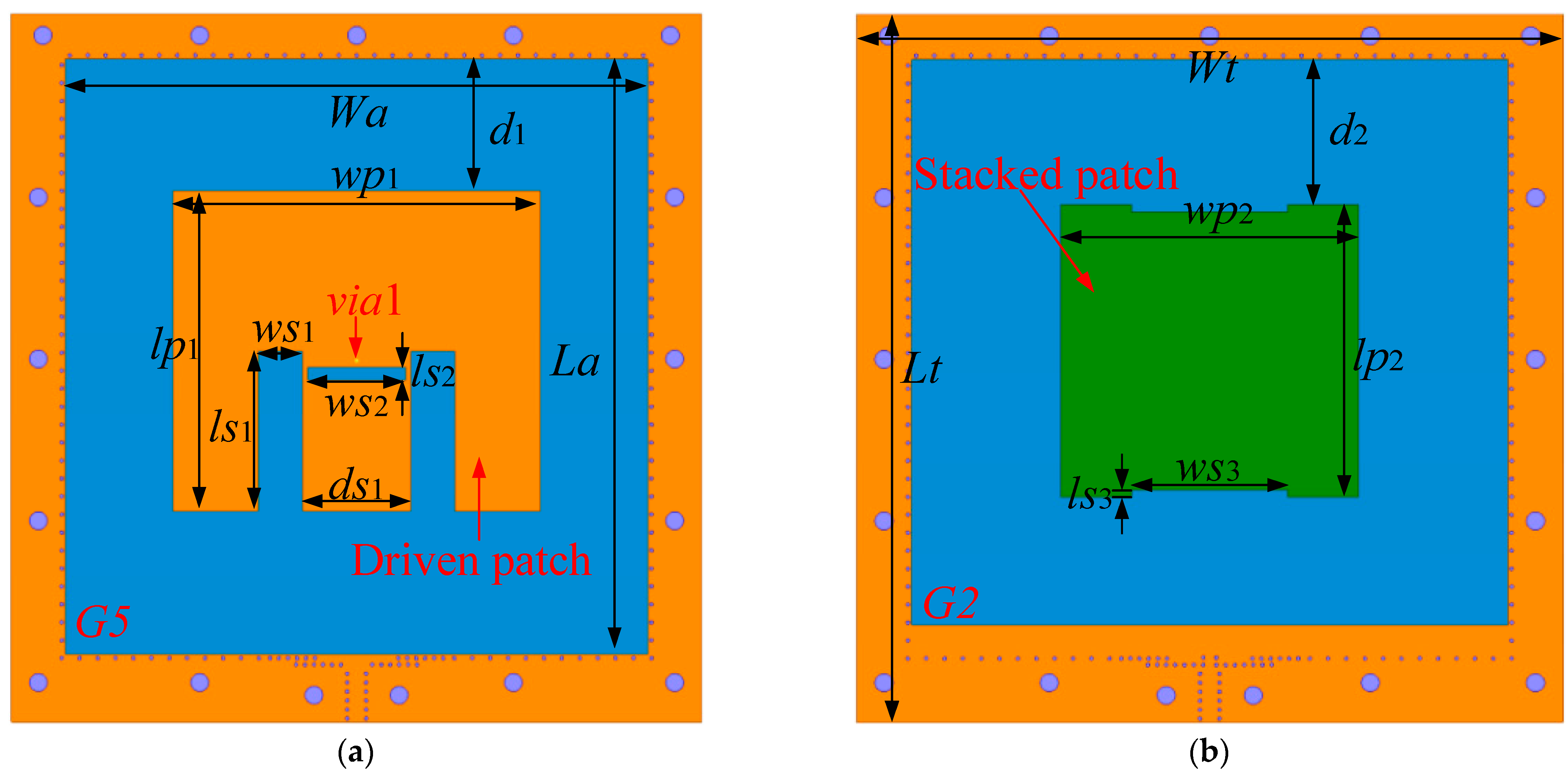
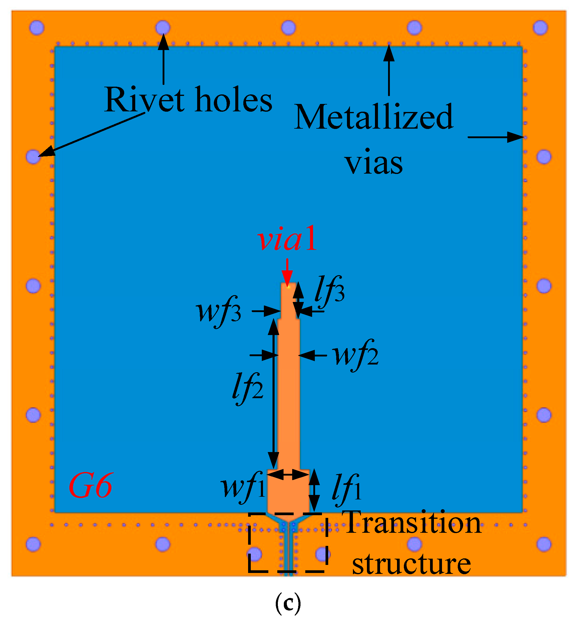
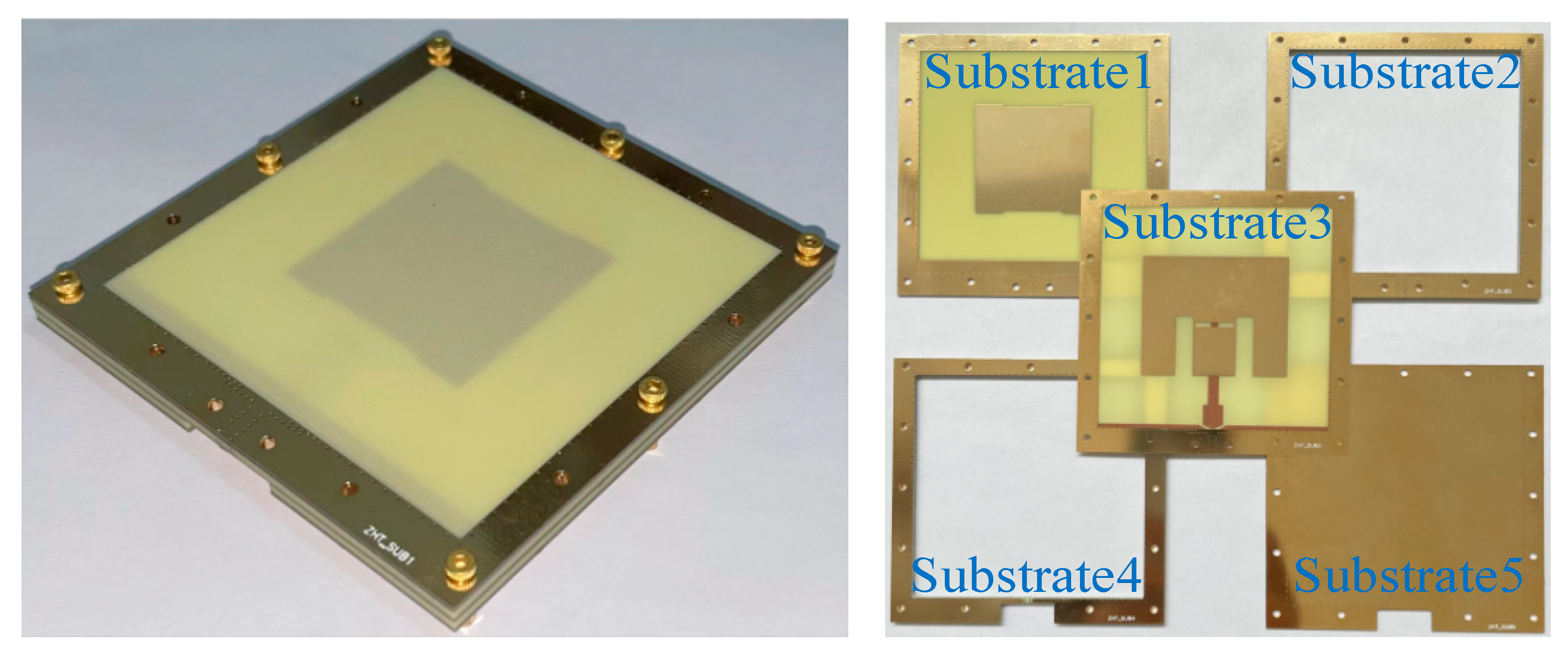
2.1. Configuration

The layout configuration of the filtering antenna is depicted in Figure 1. The proposed antenna uses the SISL structure consisting of five layers of the substrate (substrate1-5) and ten layers of metal (G1–G10) as the design platform. All five layers of substrate are made of FR4 epoxy materials with meagre cost, the thickness of each layer is h1 of 0.6 mm, h2 of 2 mm, h3 of 0.127 mm. The hollow parts of substrate2 and substrate4 are two air cavities, where most of the electric field is distributed, resulting in very low dielectric loss. The core circuit is designed on the dielectric substrate 3, and the dielectric substrate 1 and 5 are utilized as cover plates. The metallized vias surround each layer of substrates. The rivet holes are arranged at the outermost part of the substrates to facilitate the assembly of the physical model.
Figure 2 exhibits the specific configuration and parameters of the antenna on the G6 layer, G2 layer, and G5 layer. As depicted in Figure 2a, a rectangular driven patch is placed on the G5 layer, and a pair of symmetrical longitudinal I-slot (slot1) and a transverse I-slot (slot3) are etched on the driven patch. The square stacked patch with strip groove (slot2) etched on the edge is placed on the G2 layer, as evidenced in Figure 2b. In Figure 2c, a segmented feed line is placed on the G6 layer, and the metallized via (via1) through the substrate3 connects the driven patch with the feed line.

2.2. Antenna Analysis

Figure 3 expresses the design steps of the proposed antenna structure. The simulated S11 and realized gain of the antenna in each step are depicted in Figure 4.
Initially, only the traditional rectangular driven patch is placed on the G5 layer, which is Ant1 in Figure 3a. It is manifest from Figure 4 that Ant1 generates a resonant frequency f2 at 3.68 GHz, and there is no radiation null. For the purpose of increasing the bandwidth and achieving the filtering response, additional resonances and radiation nulls should be led into. Therefore, the rectangular driven patch is deformed, and a couple of slots (slot1) are symmetrically etched on the conventional rectangular driven patch, as shown in the Ant2 in Figure 3b. It can be seen from Figure 4 that the S11 and realized gain of Ant 2 have changed significantly, and a new resonance frequency point f1 is generated at 3.3 GHz, but the matching of this point is poor. At this time, f2 is not easy to be observed because of serious mismatch. A radiation null n1 is produced at 2.92 GHz.
Then, based on Ant2, the grooved stacked patch on the G2 layer is loaded, which is called Ant3, as shown in Figure 3c. Ant3 generates the third resonant frequency f3 at 3.9 GHz, and the matching of f1 and f2 is improved. Moreover, two new radiation nulls, n2 and n3, are generated at 4.34 GHz and 4.78 GHz. The bandwidth of the antenna band has been initially broadened, and the antenna frequency selection feature has been initially realized, but the matching of f3 is relatively poor, the frequency at the radiation null n1 moves to the low frequency. The out-of-band suppression level in the low-frequency band has been slightly reduced. The out-of-band suppression level in the high-frequency band is relatively high, but the roll-off rate needs to be improved.
Finally, an I-slot (slot3) is etched on the driven patch for optimal matching to get the proposed antenna, as exhibited in Figure 3d. In Figure 4, the matching of f3 is significantly improved. Moreover, n2 move to the lower frequency direction, resulting in high selectivity. The out-of-band suppression level in the low-frequency band has decreased somewhat. The out-of-band suppression level in the high-frequency band is relatively high, but the roll-off rate has been somewhat improved. The simulation impedance bandwidth of the proposed antenna is 18% and peak gain is 8.97 dBi.
In addition, the impedance plot of a given frequency band is given. The impedance plot for the given frequency band is shown in Figure 5. In the frequency band of 3.24–3.88 GHz, the real part of the antenna impedance is around 50 Ω and the imaginary part is around 0, achieving impedance matching. However, at other frequencies, there is impedance mismatch, revealing the antenna’s filtering response.

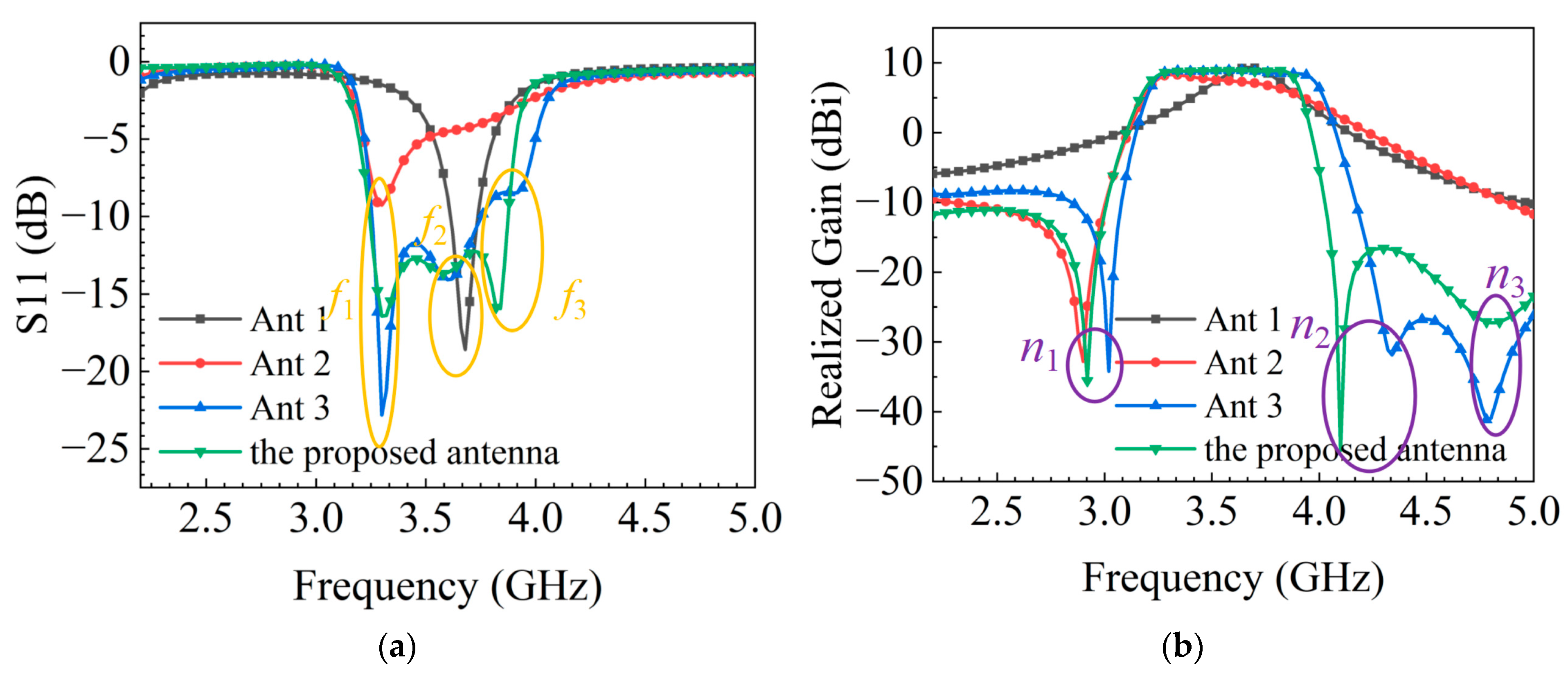
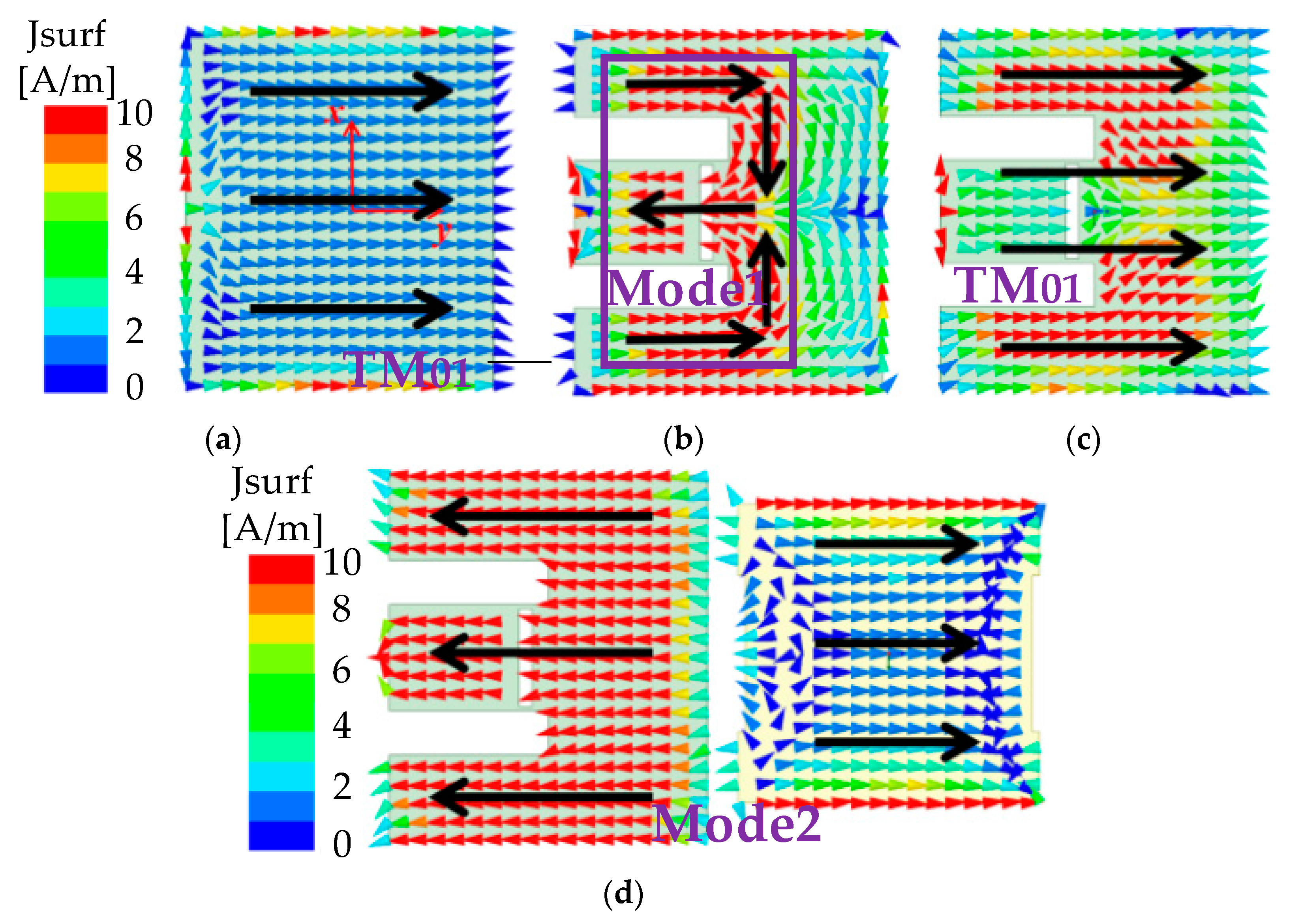
2.2.1. Three Resonance Frequencies

Figure 6b–d presents the surface current distribution and current path diagram at three resonance frequencies of the proposed antenna to visually compare the change of resonance mode in the design steps.
Since the proposed antenna is developed from the traditional rectangular microstrip antenna, the operating mode of the radiation patch of Ant1 at resonance frequency f2 is TM01 mode, as expressed in Figure 6a. As exhibited in Figure 6b, the current at the resonance frequency f1 is mainly distributed around slot1, so mode 1 results from slot1 on the driven patch. The initial mode TM01 of the driven patch at resonance frequency f2 is plotted in Figure 6c. The resonance frequency f3 is generated after loading the stacked patch. According to Figure 6d, its operating mode2 at resonance frequency indicates that the driven patch and the stacked patch are coupled together to generate resonance frequency f3.

2.2.2. Three Radiation Nulls

In Figure 7, the surface current distributions at n1, n2, and n3 are presented to explain the cause of radiation nulls. Figure 7a indicates that the current on the driven patch is primarily concentrated around slot1, with equal current amplitude on both sides of slot1 but in opposite directions. This weakens the radiation effect on the driven patch and generates radiation null n1. After loading the stacked patch, radiation nulls n2 and n3 are generated. Figure 7b shows that at n2, the surface current direction of the driven patch and the stacked patch is opposite, resulting in the maximum suppression of radiation energy on the driven patch and the generation of radiation null n2. Similarly, in Figure 7c, a robust current distribution occurs in the center of the driven patch and the stacked patch at n3, with opposite current directions in these two parts. This cancels out the radiation energy and produces radiation null n3. In conclusion, the electromagnetic radiation at the corresponding frequency is canceled, resulting in radiation nulls. The gain decreases rapidly on both sides of the frequency band, achieving a good roll-off rate and realizing the filtering characteristics of the antenna.

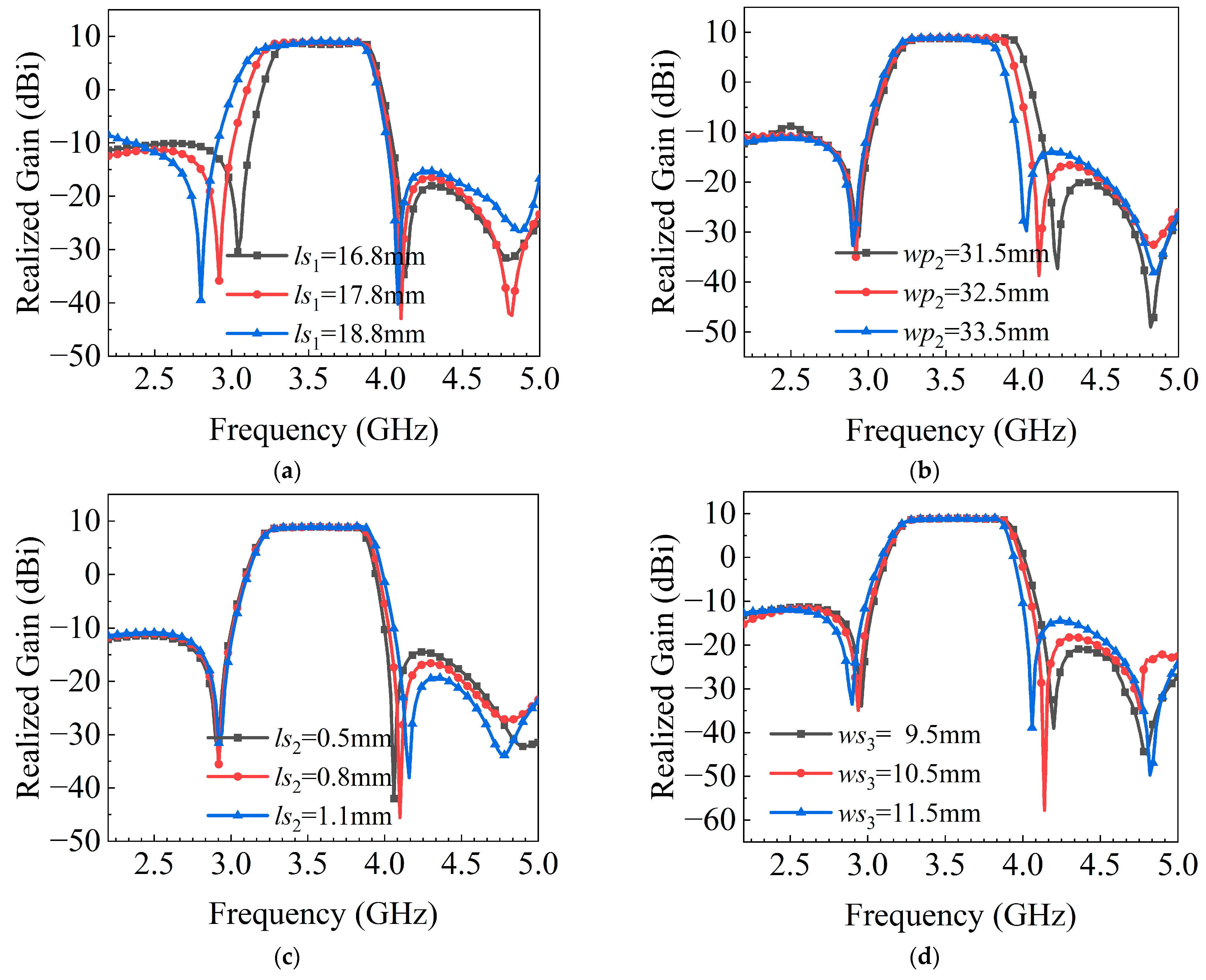
2.2.3. Analysis of Critical Parameters

The critical parameters of the driven patch, stacked patch and slots are analyzed one by one. Figure 8a shows that the decrease of the length ls1 of slot1 makes f1 shift to a higher frequency direction, which verifies that f1 is generated by slot1. At the same time, because the length change of slot1 will have some influence on the current distribution of the driven patch, it will affect the matching of f2. Figure 8b plots the influence of the width lp1 of the driven patch on the S11. The change of lp1 has the most significant influence on the matching of the resonance frequency f2, the matching of f2 worsens as the increase of lp1. Figure 8c can prove that f3 is affected by the width wp2 of the stacked patch. With the increase of wp2, f3 shifts to the lower frequency direction, and the matching becomes poor. It has some influence on the resonance frequency f2.
Figure 9 shows the effects of some parameters on radiation nulls. The radiation null n1 moves to a lower frequency direction with the growth of ls1, as illustrated in Figure 9a. The radiation null n2 moves to a lower frequency direction with increasing of wp2 and a higher frequency direction with increasing of ls2, as demonstrated in Figure 9b,c. The changes of wp2 and ls2 also affect the out-of-band suppression level at high frequencies. Figure 9d displays the effect of the length ws3 of slot3 on the radiation null. Both n1 and n2 shift to a lower frequency direction as ws3 increases, confirming the effect of adding slot3 on n1 and n2 in Figure 4b. Ls2 and ws3 affects the current distribution at 4.84 GHz, resulting in the movement of n3, as shown in Figure 9c,d. The proposed antenna is simulated and optimized by ANSYS software, and the optimized parameters are shown in Table 1.

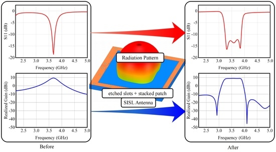
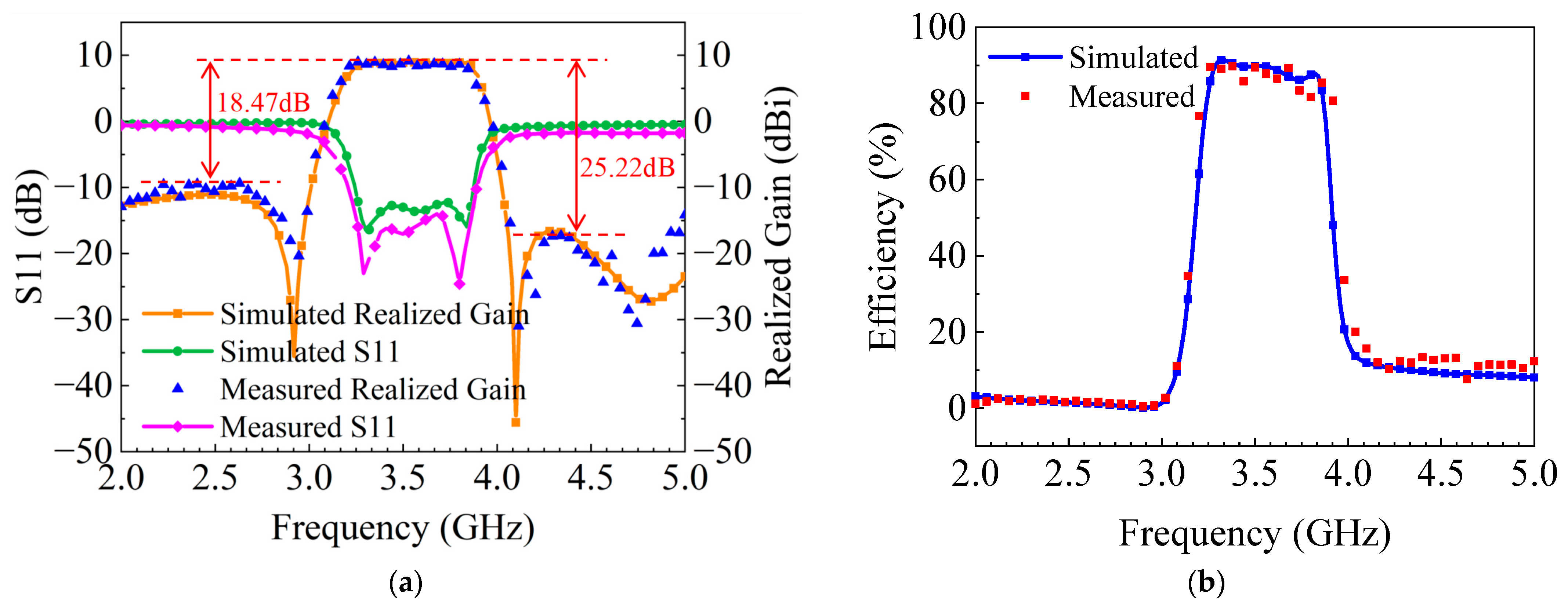
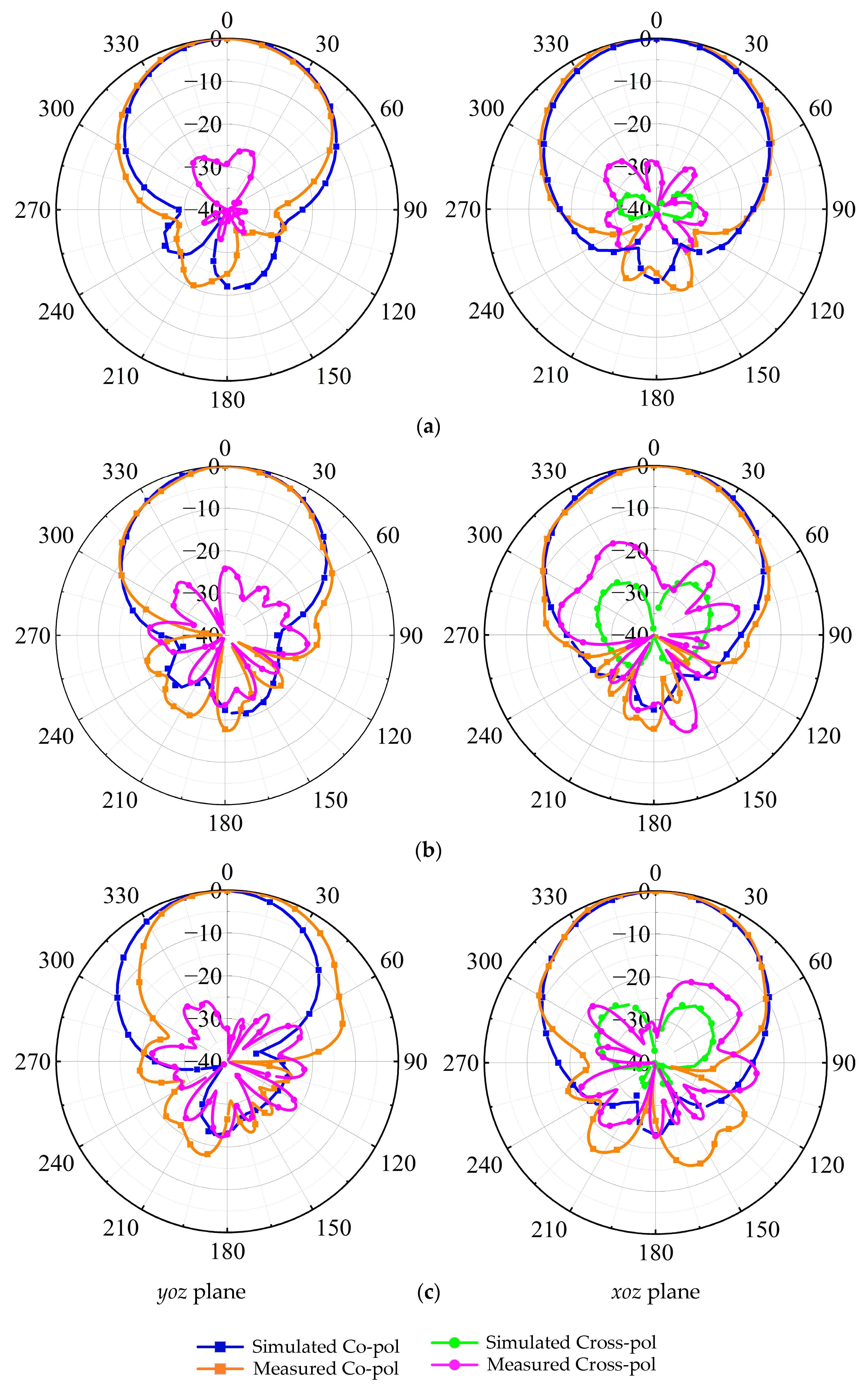
3. Antenna Measurement and Discussion

The proposed filtering antenna is fabricated and measured. Figure 10 exhibits the pictures of the manufactured filtering antenna. The simulation results and measurement results of the proposed antenna are illustrated in Figure 11. It can be concluded that the measurement impedance bandwidth is 19.5% (3.2–3.89 GHz), which is wider than the simulation result of 18% (3.24–3.88 GHz), and the impedance matching is also improved compared with the simulation result. The maximum measured gain at 3.25 GHz is 9.21 dBi. Three measured radiation nulls are located at 2.94 GHz, 4.1 GHz, and 4.74 GHz, respectively. The out-of-band suppression levels of 18.47 dB and 25.22 dB are reached in upper and lower frequency bands and have high roll-off rates, resulting in higher frequency selectivity. Figure 11b shows that the maximum efficiency of the antenna in the frequency band can reach 93.5%. The errors between measurement and simulation results may come from assembly errors and measurement environment. The simulated and measured normalized radiation patterns in the yoz and xoz plane of the proposed antenna at 3.3 GHz, 3.58 GHz, and 3.84 GHz are shown in Figure 12. The proposed filtering antenna has good radiation characteristics in the working frequency band. The measurement results show better than normal consistency with the simulation results. Because the simulated cross-polarization is small, it is not displayed in the radiation patterns of yoz plane.
The comparisons with other works are exhibited in Table 2. The bandwidth of the proposed antenna (19.5%) can be kept at a high level compared to [11,17,20,23]. The gain (9.21 dBi) is higher than [11,16,17,20,21,22,23,24]. The minimum out-of-band rejection level is 18.47 dB, which is better than most antennas except for [26]. The processing cost of the antenna is lower than that of other reference antennas by using FR4 material. However, the antenna proposed in this work has a relatively larger size.

4. Conclusions

This paper introduces an SISL-based 5G filtering patch antenna with wide bandwidth, high gain, and high selectivity. Instead of using a filter or filtering circuit, the antenna utilizes the design method of etching slots and stacked patch to achieve the desired filtering characteristics. The introduction of two new modes results in a filtering response with three radiation nulls, leading to bandwidth enhancement and high selectivity. The antenna has the properties of low cost, excellent radiation performance, and frequency selectivity, making it suitable for application in 5G communication systems. In the future, methods such as loading branches, pins, or further improving patch shapes will be considered in the design of antenna improvements to enhance the suppression level in the low-frequency band, promote antenna miniaturization, reduce the volume of 5G communication systems, improve system performance, and further reduce manufacturing costs.

Author Contributions

Concept and structure of SISL (dielectric integrated suspension line), K.M.; design ideas, H.Z. and N.Y.; software simulation and parameter optimization, H.Z.; data processing, H.Z.; data curation, N.Y. and K.M.; writing—original draft preparation, H.Z. and N.Y.; writing—review and editing, N.Y. and K.M.; supervision, N.Y. and K.M. All authors have read and agreed to the published version of the manuscript.

Funding

This work was supported in part by the National Natural Science Foundation of China Key Project, grant number 61831017; and in part by the National Natural Science Foundation of China, grant number 62001324.

Informed Consent Statement

Not applicable.

Data Availability Statement

The datasets used and/or analyzed during the current study are available from the corresponding author on reasonable request.

Conflicts of Interest

The authors declare no conflict of interest.

References

  1. Wu, P.-C.; Chen, L.; Luo, Y.-L. Miniaturised wideband filtering antenna by employing CRLH-TL and simplified feeding structure. Electron. Lett. 2015, 51, 548–550. [Google Scholar] [CrossRef]
  2. Sun, G.H.; Wong, S.W.; Zhu, L.; Chu, Q.X. A compact printed filtering antenna with good suppression of upper harmonic band. IEEE Antennas Wirel. Propag. Lett. 2016, 15, 1349–1352. [Google Scholar] [CrossRef]
  3. Ma, Z.K.; Vandenbosch, G.A.E. Wideband harmonic rejection filtenna for wireless power transfer. IEEE Trans. Antennas Propag. 2014, 62, 371–377. [Google Scholar] [CrossRef]
  4. Deng, J.; Hou, S.; Zhao, L.; Guo, L. A Reconfigurable Filtering Antenna with Integrated Bandpass Filters for UWB/WLAN Applications. IEEE Trans. Antennas Propag. 2018, 66, 401–404. [Google Scholar] [CrossRef]
  5. Li, L.; Liu, G. A differential microstrip antenna with filtering response. IEEE Antennas Wirel. Propag. Lett. 2016, 15, 1983–1986. [Google Scholar] [CrossRef]
  6. Mao, C.X.; Zhang, L.; Khalily, M.; Gao, Y.; Xiao, P. A multiplexing filtering antenna. IEEE Trans. Antennas Propag. 2021, 69, 5066–5071. [Google Scholar] [CrossRef]
  7. Wei, Z.H.; Zhou, Z.; Tang, Z.Y.; Yin, J.Y.; Ren, J.; Yin, Y.Z. Broadband filtering magnetoelectronic dipole antenna with quasi-elliptic gain response. IEEE Trans. Antennas Propag. 2020, 68, 3225–3230. [Google Scholar] [CrossRef]
  8. Tang, M.-C.; Li, D.J.; Wang, Y.; Hu, K.-Z.; Ziolkowski, R.W. Compact, low-profile, linearly and circularly polarized filtennas enabled with custom-designed feed-probe structures. IEEE Trans. Antennas Propag. 2020, 68, 5247–5256. [Google Scholar] [CrossRef]
  9. Liu, Y.-T.; Leung, K.W.; Yang, N. Compact absorptive filtering patch antenna. IEEE Trans. Antennas Propag. 2020, 68, 633–642. [Google Scholar] [CrossRef]
  10. Jin, J.Y.; Liao, S.W.; Xue, Q. Design of Filtering-Radiating Patch Antennas with Tunable Radiation Nulls for High Selectivity. IEEE Trans. Antennas Propag. 2018, 66, 2125–2130. [Google Scholar] [CrossRef]
  11. Liu, Q.W.; Zhu, L. A Compact Wideband Filtering Antenna on Slots-Loaded Square Patch Radiator under Triple Resonant Modes. IEEE Trans. Antennas Propag. 2022, 70, 9882–9887. [Google Scholar] [CrossRef]
  12. Chen, C.L. A Wideband Coplanar L-Probe-Fed Slot-Loaded Rectangular Filtering Microstrip Patch Antenna with High Selectivity. IEEE Antennas Wirel. Propag. Lett. 2022, 21, 1134–1138. [Google Scholar] [CrossRef]
  13. Zhang, Y.; Zhang, X.Y.; Liu, Q.H. A Dual-Layer Filtering SIW Slot Antenna Utilizing Double Slot Coupling Scheme. IEEE Antennas Wirel. Propag. Lett. 2021, 20, 1073–1077. [Google Scholar] [CrossRef]
  14. Li, J.F.; Chen, Z.N.; Wu, D.L.; Zhang, G.; Wu, Y.-J. Dual-Beam Filtering Patch Antennas for Wireless Communication Application. IEEE Trans. Antennas Propag. 2018, 66, 3730–3734. [Google Scholar] [CrossRef]
  15. Yang, W.-J.; Pan, Y.-M.; Zhang, X.-Y. A single-layer low-profile circularly polarized filtering patch antenna. IEEE Antennas Wirel. Propag. Lett. 2021, 20, 602–606. [Google Scholar] [CrossRef]
  16. Wong, S.W.; Huang, T.G.; Mao, C.X.; Chen, Z.N.; Chu, Q.X. Planar Filtering Ultra-Wideband (UWB) Antenna with Shorting Pins. IEEE Trans. Antennas Propag. 2013, 61, 948–953. [Google Scholar] [CrossRef]
  17. Yang, W.; Xun, M.; Che, W.; Feng, W.; Zhang, Y.; Xue, Q. Novel compact high-gain differential-fed dual-polarized filtering patch antenna. IEEE Trans. Antennas Propag. 2019, 67, 7261–7271. [Google Scholar] [CrossRef]
  18. Hu, K.-Z.; Tang, M.-C.; Li, D.; Wang, Y.; Li, M. Design of compact, single-layered substrate integrated waveguide filtenna with parasitic patch. IEEE Trans. Antennas Propag. 2020, 68, 1134–1139. [Google Scholar] [CrossRef]
  19. Yang, D.; Zhai, H.Q.; Guo, C.Z.; Li, H.K. A Compact Single-Layer Wideband Microstrip Antenna with Filtering Performance. IEEE Antennas Wirel. Propag. Lett. 2020, 19, 801–805. [Google Scholar] [CrossRef]
  20. Zhang, B.H.; Xue, Q. Filtering Antenna with High Selectivity Using Multiple Coupling Paths from Source/Load to Resonators. IEEE Trans. Antennas Propag. 2018, 66, 4320–4325. [Google Scholar] [CrossRef]
  21. Chen, B.-J.; Yang, X.-S.; Wang, B.-Z. A Compact High-Selectivity Wideband Filtering Antenna with Multipath Coupling Structure. IEEE Antennas Wirel. Propag. Lett. 2022, 21, 1654–1658. [Google Scholar] [CrossRef]
  22. Hu, H.-T.; Chan, C.H. Substrate-Integrated-Waveguide-Fed Wideband Filtering Antenna for Millimeter-Wave Applications. IEEE Trans. Antennas Propag. 2021, 69, 8125–8135. [Google Scholar] [CrossRef]
  23. Kulkarni, P.; Srinivasan, R. Compact polarization diversity patch antenna in L and WiMAX bands for IoT applications. AEU-Int. J. Electron. C 2021, 136, 153772. [Google Scholar] [CrossRef]
  24. Kulkarni, J.; Sim, C.Y.D.; Poddar, A.; Rohde, U.L.; Alharbi, A.G. A Compact Circularly Polarized Rotated L-Shaped Antenna with J-Shaped Defected Ground Strucutre for WLAN and V2X Applications. Prog. Electrom. Res. Lett. 2022, 102, 135–143. [Google Scholar] [CrossRef]
  25. Wang, T.; Yan, N.N.; Tian, M.; Luo, Y.; Ma, K.X. A Low-Cost High-Gain Filtering Patch Antenna with Enhanced Frequency Selectivity Based on SISL for 5G Application. IEEE Antennas Wirel. Propag. Lett. 2022, 21, 1772–1776. [Google Scholar] [CrossRef]
  26. Tian, M.; Yan, N.N.; Luo, Y.; Ma, K.X. A Low-Cost High-Gain Filtering Patch Antenna Using SISL Technology for 5G Application. IEEE Antennas Wirel. Propag. Lett. 2021, 20, 2270–2274. [Google Scholar] [CrossRef]
  27. Aminu, S.; Yan, N.N.; Luo, Y.; Ma, K.X. Bandwidth improvement of patch antenna and array with out-of-band rejection based on SISL platform for 5G applications. Microw. Opt. Technol. Lett. 2022, 64, 1455–1461. [Google Scholar] [CrossRef]
  28. Hao, J.; Yan, N.N.; Luo, Y.; Fu, H.; Ma, K.X. A Low-Cost Dual-Band Multimode High-Gain Stacked-Patch Antenna Based on SISL for 5G Applications. IEEE Antennas Wirel. Propag. Lett. 2022, 21, 4–8. [Google Scholar] [CrossRef]
  29. Yan, N.; Song, D.; Luo, Y.; Ma, K. A Low-Cost Miniaturized Filtering Dielectric Resonator Antenna Based on SISL for 5G Application. IEEE Trans. Antennas Propag. 2022, 70, 11344–11352. [Google Scholar] [CrossRef]
  30. Luo, Y.; Yin, T.; Yan, N.; An, W.; Ma, K. A Low-Cost Differentially Fed Dual-Mode Filtering MIMO Antenna with Enhanced Isolation Based on SISL Platform. IEEE Antennas Wirel. Propag. Lett. 2022, 21, 198–202. [Google Scholar] [CrossRef]
Figure 1. Layout view of the filtering antenna.
Electronics 12 01331 g001
Figure 2. Configurations at each layer. (a) G5 layer; (b) G2 layer; (c) G6 layer.
Electronics 12 01331 g002aElectronics 12 01331 g002b
Figure 3. Reference antennas. (a) Ant1; (b) Ant2; (c) Ant3 and (d) the proposed antenna.
Electronics 12 01331 g003
Figure 4. Simulated results for the reference and proposed antennas. (a) S11; (b) realized gain.
Electronics 12 01331 g004
Figure 5. Simulated input impedance plot of the proposed antenna.
Electronics 12 01331 g005
Figure 6. Current distributions and current paths. (a) TM01 mode of Ant1; (b) Mode1 at f1, 3.3 GHz; (c) TM01 at f2, 3.58 GHz; (d) Mode2 at f3, 3.84 GHz.
Electronics 12 01331 g006
Figure 7. Current distributions and current paths of the three radiation nulls. (a) n1, 2.92 GHz; (b) n2, 4.1 GHz; (c) n3, 4.78 GHz.
Electronics 12 01331 g007
Figure 8. Simulated S11 for different parameters. (a) ls1; (b) lp1; (c) wp2.
Electronics 12 01331 g008
Figure 9. Simulated gain for different parameters. (a) ls1; (b) wp2; (c) ls2; (d) ws3.
Electronics 12 01331 g009
Figure 10. Prototype of the proposed antenna.
Electronics 12 01331 g010
Figure 11. Simulated and measured results of the proposed antenna. (a) S11 and realized gain; (b) efficiency.
Electronics 12 01331 g011
Figure 12. Radiation patterns at different frequencies. (a) 3.3 GHz. (b) 3.58 GHz. (c) 3.84 GHz.
Electronics 12 01331 g012
Table 1. Optimized antenna dimension. (Unit: mm).
ParameterValueParameterValueParameterValue
Wt77lp135.6ls31.5
Lt78.8wp141ws311
Wa65lp232.5lf16
La66.3wp232.5wf15.8
La163ls117.8lf221
d114.7ws15wf23.1
d220.125ls20.8lf35
ds111ws217wf32.1
h10.6h22h30.127
Table 2. Comparisons with other filtering antenna.
Ref.Bandwidth (GHz)Peak Gain
(dBi)
Rejection Level (dB)Size (λ03)Material
[11]3.34–3.66 (9.14%)7.612.70.457 × 0.457 × 0.043F4B
[16]2.3–2.9 (23%)8.9200.8 × 0.8 × 0.06None
[17]2.705–2.847 (5.1%)6.3None0.76 × 0.44 × 0.015Taconic TLY-5
[20]2.15–2.5 (15.2%)5.2130.66 × 0.62 × 0.062RO4003C
[21]4.45–5.52 (21.5%)4.815.90.4 × 0.4 × 0.09F4BM
[23]1.575 (3.5%) &
3.4–3.6 (5.71%)
3.15 & 4.3None0.13 × 0.13 × 0.067ARLON 1000
[24]4.8–5.99 (22.05%)2.5None0.55 × 0.55 × 0.014FR4
[26]4.28–5.34 (22.04%)10.414.50.78 × 0.8 × 0.08FR4
This3.2–3.89 (19.5%)9.2118.470.93 × 0.91 × 0.06FR4
Disclaimer/Publisher’s Note: The statements, opinions and data contained in all publications are solely those of the individual author(s) and contributor(s) and not of MDPI and/or the editor(s). MDPI and/or the editor(s) disclaim responsibility for any injury to people or property resulting from any ideas, methods, instructions or products referred to in the content.

