Article

Research on Five-Level PFC Circuit Topology Based on Switch-Diode-Capacitor Network

College of Electrical Engineering and New Energy, China Three Gorges University, No. 8 Daxue Road, Yichang 443002, China
*
Authors to whom correspondence should be addressed.
Electronics 2023, 12(6), 1286; https://doi.org/10.3390/electronics12061286
Submission received: 10 February 2023 / Revised: 28 February 2023 / Accepted: 5 March 2023 / Published: 8 March 2023

Abstract

:
In this paper, a family of a novel single-phase three-level PFC based on a switch-capacitor cell is proposed. The proposed PFC topologies have the characteristics of high power factor, low voltage stresses, and low power losses. Firstly, the derivation process of the novel PFC topologies is introduced in detail. Based on a representative circuit of the proposed novel PFC topologies, its operation principle is analyzed from the aspects of working current paths, key waveforms, and pulse distribution. Meanwhile, its equivalent circuit model is deduced. Secondly, the performance of the proposed PFC topologies is analyzed. Then the modulation technology based on capacitor voltage balancing is designed for the proposed topologies. Finally, an experimental prototype with a rated power of 800 W and a DC output voltage of 400 V is built. The experimental analysis is carried out from both the steady state and dynamic state. The experimental results verify the feasibility of the proposed novel three-level PFC topologies and the effectiveness of the modulation technology.

1. Introduction

International standards such as IEEE 519, IEC 100-3-2, and IEC61000-3-2 put forward restrictions on harmonic currents injected into the power grid by rectifiers, especially for motor drives, lighting equipment, and special industrial products [1,2,3]. The common way to meet the requirements is to use active power factor correction (APFC) rectifiers for the advantages of high power factor, continuous input current, and high efficiency [4]. However, the semiconductor devices in conventional two-level APFC rectifiers withstand excessive voltage stresses, resulting in high switching losses. To improve the efficiency, a better method is to use multilevel technology [5]. It is well known that applying multilevel technology can reduce the voltage stresses of switching devices in PFC rectifiers and effectively reduce the filter size and weight [6,7,8,9,10].
In the relevant studies on the structures of the multilevel PFC topologies, many multilevel PFC topologies with remarkable features have been developed. A novel bridgeless three-level PFC topology is proposed in [11]. This topology replaces half of the controllable switches in the traditional three-level PFC with diodes, reducing the number of active switches and improving the performance of the converter. In [12], a five-level boost PFC rectifier using a reduced number of switches is developed, which remarkably reduces the size of the manufactured box and the current harmonics. In [13], a novel single-phase five-level PFC rectifier is proposed, which has fewer active switches, a simpler drive, and lower power losses compared to similar PFC rectifiers. In order to improve the efficiency and optimize the output performance, many scholars improve the performance of multilevel PFC topology mainly from the overall multi-objective optimization of the converter [14,15,16]. The above literature optimizes the existing PFC topologies to a certain extent and improves the performance and efficiency, but the original PFC topology structures are not changed substantially.
Based on the careful analysis and summary of the above multilevel PFC topologies, a family of novel single-phase three-level PFC topologies based on switch-capacitor cells are developed in this paper. The proposed topologies enrich the existing three-level PFC topology types and have the characteristics of a low number of active switches, low power losses, and high reliability. The organization of this paper is as follows. In Section 2, the derivation process and the operation principle of the proposed novel three-level PFC topologies are presented in detail. In Section 3, the voltage stresses of power devices are analyzed. Meanwhile, the calculation and comparison of the switching device losses are given. In Section 4, the modulation technology of the proposed PFC is presented. The detailed experimental validation is given in Section 5, and the conclusions are summarized in Section 6.

2. Topology Deduction and Operation Principle

2.1. Deduction Process of Novel PFC Topologies

The traditional three-level power factor correction circuit (TTL-PFC) shown in Figure 1a uses diodes to clamp the voltage of the corresponding active switches and ensures the bidirectional flow of current [17]. However, in the application of unidirectional power flow, the number of active switches is a significant disadvantage of this approach. As shown in Figure 1b, it is a unidirectional three-level power factor correction circuit (UTL-PFC), which reduces four active switches and improves the efficiency compared to the TTL-PFC topology [11]. Unfortunately, there are four modes that have two active switches conducting at the same time among all six operating modes of the UTL-PFC, which results in the disadvantages of excessive switching losses and complexity of control.
Generally, three-level PFC topologies usually adopt capacitors in parallel on the DC side for voltage regulation [18,19,20]. According to the topology characteristics, the link structure of the switch, diode, and capacitor can be defined as a switch-capacitor cell (SCC), which is divided into two forms: common anode SCC and common cathode SCC, as shown in Figure 2.
In order to facilitate the pulse distribution and reduce the switching losses of the UTL-PFC, this paper uses the cells shown in Figure 2 to reconstruct the upper and lower controllable switch bridge arms of the UTL-PFC topology and obtains a family of a novel single-phase three-level PFC topologies, as shown in Figure 3. In Figure 3a, switch S1, the capacitor C1, and the diode D5 form a common cathode SCC. Meanwhile, the switch S2, the capacitor C2, and the diode D6 form a common anode SCC. In order to prevent the bidirectional flow of current, the diodes D3 and D4 are connected in series on the branches of switches S1 and S2, respectively. By connecting the source of the switch S2 in Figure 3a to point a or the drain of switch S1 to point a, the PFC topologies shown in Figure 3b,c can be obtained. The topology shown in Figure 3b uses only one common cathode SCC, which is composed of switch S1, diode D5, and capacitor C1. Correspondingly, only one common anode SCC is used in the topology shown in Figure 3c, which is formed by the switch S2, the diode D6, and the capacitor C2. In all three proposed PFC topologies, diodes D5 and D6 can ensure the unidirectional flow of power and prevent the energy of capacitors from returning to the input side.
The proposed three-level PFC topologies are named respectively according to the topological structure characteristics. Figure 3a–c are defined as symmetrical three-level PFC (STL-PFC), upper asymmetrical three-level PFC (UATL-PFC), and lower asymmetrical three-level PFC (LATL-PFC), respectively. Compared with the UTL-PFC topology, the proposed PFC topologies work with only one active switch at most in each operating mode, which reduces the switching losses and the difficulty of the control system design. Meanwhile, the proposed novel PFC topologies have the same switching pulse signal distribution, which means they can use the same modulation method.

2.2. Operation Principle of Novel PFC Topologies

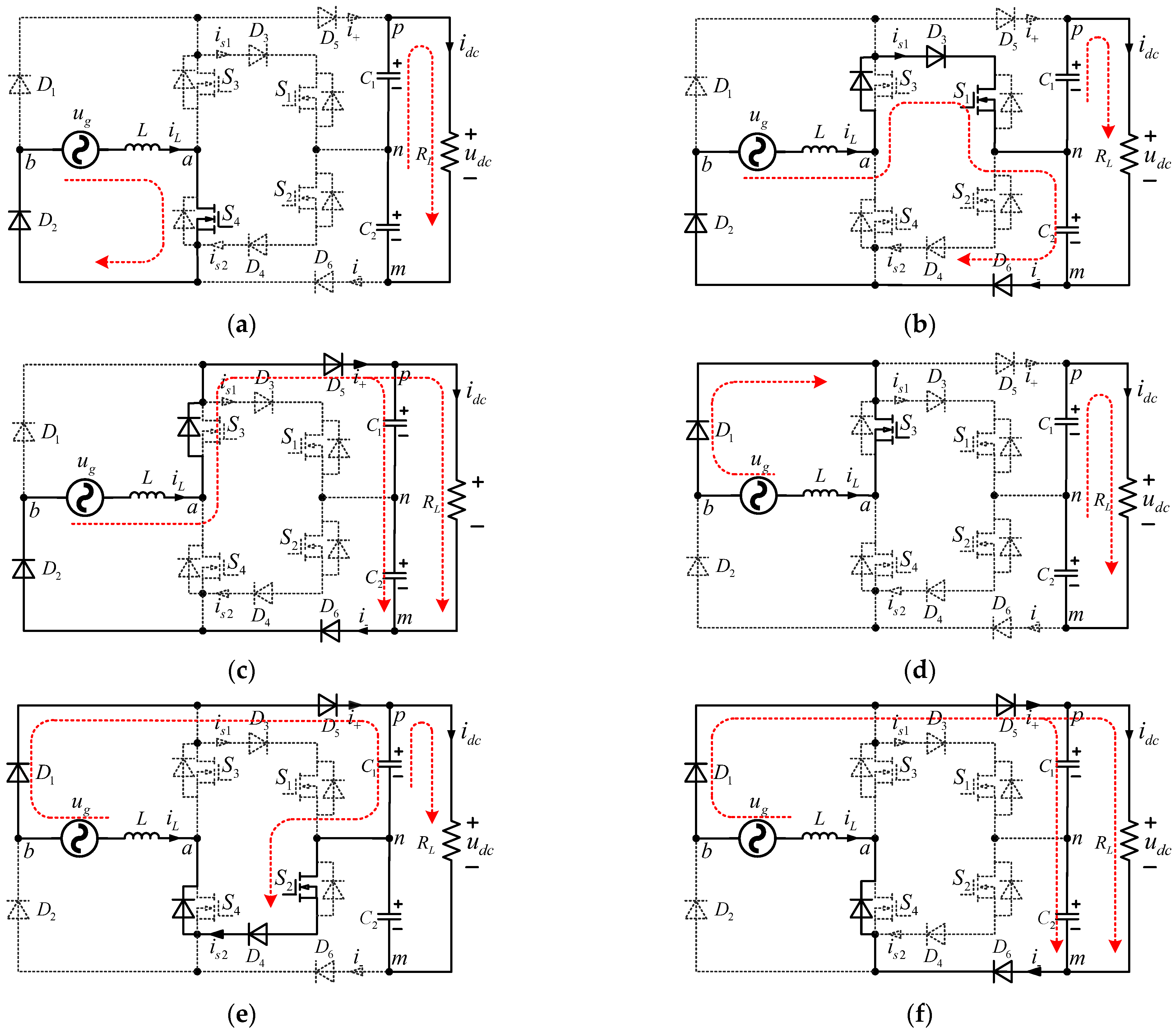
As the pulse signal distribution of the STL-PFC, UATL-PFC, and LATL-PFC is the same, this section takes the STL-PFC topology as an example to analyze the operation principle, and other proposed topologies can be analyzed in the same way. The STL-PFC topology is formed by an AC voltage source ug, one inductor L, four switches S1S4, six diodes D1D6, and two identical capacitors C1C2. The STL-PFC has six operating modes in one power frequency period at a steady state, and the current path corresponding to each operating mode is shown in Figure 4. The key waveforms of the STL-PFC topology during one power frequency period are shown in Figure 5. The analysis of each operating mode is given as follows.
Mode 1 [t∈(t0,t1)∪(t2,t3)]: Only the switch S4 is turned ON as shown in Figure 4a. The inductor L is in the energy storage state. Meanwhile, the capacitors C1 and C2 supply power to the load RL. During this state, the voltage uab = +0. The equation of this mode can be expressed as:
L d i L / d t = u g
Mode 2 [t∈(t0,t3)]: Only the switch S1 is turned ON, as shown in Figure 4b. In this mode, the capacitor C2 is charged, the capacitor C1 provides energy to the load RL, and the voltage uab = +uc2 = +0.5udc. During this state, if the power supply voltage is higher than 0.5udc, the inductor current iL increases linearly. Correspondingly, if the power supply voltage is lower than 0.5udc, the inductor current iL decreases linearly. The equation of this mode can be obtained as follows:
L d i L / d t = u g u d c / 2
Mode 3 [t∈(t1,t2)]: All switches are turned OFF, as shown in Figure 4c. During this state, the inductor L provides energy to the load RL. At the same time, the capacitors C1 and C2 are charged, and the voltage uab = uc1 + uc2 = udc. The equation of this mode can be obtained as follows:
L d i L / d t = u g u d c
Mode 4 [t∈(t3,t4)∪(t5,t6)]: Only the switch S3 is turned ON, as shown in Figure 4d. The inductor current iL increases linearly. Meanwhile, the capacitors C1 and C2 supply power to the load RL, the voltage uab = −0. The equation of this mode can be obtained as follows:
L d i L / d t = u g
Mode 5 [t∈(t3,t6)]: Only the switch S2 is turned ON as shown in Figure 4e. In this mode, the capacitor C1 is charged, the capacitor C2 discharges energy to the load RL, and the voltage uab = −uc1 = −0.5udc. During this state, if the absolute value of the power supply voltage is higher than 0.5udc, the inductor current iL increases linearly. Correspondingly, if the absolute value of the power supply voltage is lower than 0.5udc, the inductor current iL decreases linearly; the equation of this mode can be obtained as:
L d i L / d t = u g u d c / 2
Mode 6 [t∈(t4,t5)]: All switches are turned OFF, as shown in Figure 4f. In this mode, the capacitors C1 and C2 are charged, the inductor current iL decreases linearly, and the voltage uab = -uc1uc2 = −udc. The equation of this mode can be obtained as follows:
L d i L / d t = u g u d c

2.3. Equivalent Circuit Model

According to the detailed analysis of the operation principle of the STL-PFC topology in Section 2.2, the switching pulse distribution and system parameters of the STL-PFC can be summarized in Table 1, where the “ON” and “OFF” states of the switches are represented by “1” and “0”, respectively. The currents i+ and i represent the upper and lower DC bus currents, respectively. The branch currents is1 and is2 represent the currents flowing through the switches S1 and S2, respectively. From Table 1, the upper DC bus current i+ is not equal to zero in modes 3, 5, and 6. Correspondingly, the lower DC bus current i is not equal to zero in modes 2, 3, and 6. The branch current is1 is not equal to zero only in mode 2.
Meanwhile, the branch current is2 is not equal to zero only in mode 5. Based on the above analysis, the currents i+, i, is1, and is2 can be calculated as:
i + = S ¯ 1 S ¯ 2 S ¯ 3 S ¯ 4 1 + sgn ( i L ) 2 i L S ¯ 3 S ¯ 4 1 sgn ( i L ) 2 i L = ( A B ) i L
i = S ¯ 2 S ¯ 3 S ¯ 4 1 + sgn ( i L ) 2 i L S ¯ 1 S ¯ 2 S ¯ 3 S ¯ 4 1 sgn ( i L ) 2 i L = ( C D ) i L
i s 1 = S 1 S ¯ 2 S ¯ 3 1 + sgn ( i L ) 2 i L S ¯ 1 S ¯ 2 S ¯ 3 1 sgn ( i L ) 2 i L S ¯ 1 S ¯ 2 S ¯ 3 S ¯ 4 1 sgn ( i L ) 2 i L = ( E F D ) i L
i s 2 = S ¯ 1 S ¯ 2 S ¯ 3 1 sgn ( i L ) 2 i L S ¯ 3 S ¯ 4 1 sgn ( i L ) 2 i L = ( F B ) i L
where:
A = S ¯ 1 S ¯ 2 S ¯ 3 S ¯ 4 1 + sgn ( i L ) 2 ,   B = S ¯ 3 S ¯ 4 1 sgn ( i L ) 2 , C = S ¯ 2 S ¯ 3 S ¯ 4 1 + sgn ( i L ) 2 ,   D = S ¯ 1 S ¯ 2 S ¯ 3 S ¯ 4 1 sgn ( i L ) 2 , E = S 1 S ¯ 2 S ¯ 3 1 + sgn ( i L ) 2 ,   F = S ¯ 1 S ¯ 2 S ¯ 3 1 sgn ( i L ) 2 , sgn ( i L ) = { 1 ,   if   i L > 0   1 ,   if   i L < 0 .
It can be seen from Table 1 that the bridge-arm voltage uab has five different levels during one power frequency period so that the voltage uab can be expressed as:
u a b = ( A B ) u c 1 + ( E + A D ) u c 2
Through different combinations of A, B, D, and E, the bridge-arm voltage uab can be converted between the five levels of udc, udc/2, 0, −udc/2, and −udc. According to (7)–(11), the equivalent circuit model of the STL-PFC topology can be obtained, as shown in Figure 6, where rL is the parasitic resistance of the inductor. The equivalent model shown in Figure 6 is also applicable to the UATL-PFC and the LATL-PFC.

3. Performance Analysis of the Proposed Topologies

3.1. Analysis of Voltage Stresses of Switching Devices

The maximum voltage stresses of the switching devices in the proposed three-level PFC topologies are analyzed under the condition of the same output power level, and the results are summarized in Table 2. It can be seen from Table 2 that the maximum voltage stresses of switches S1 and S2 in the switch-capacitor cells of all three proposed PFC topologies are halved, which is beneficial for reducing the switching losses.

3.2. Calculation and Comparison of the Switching Device Losses

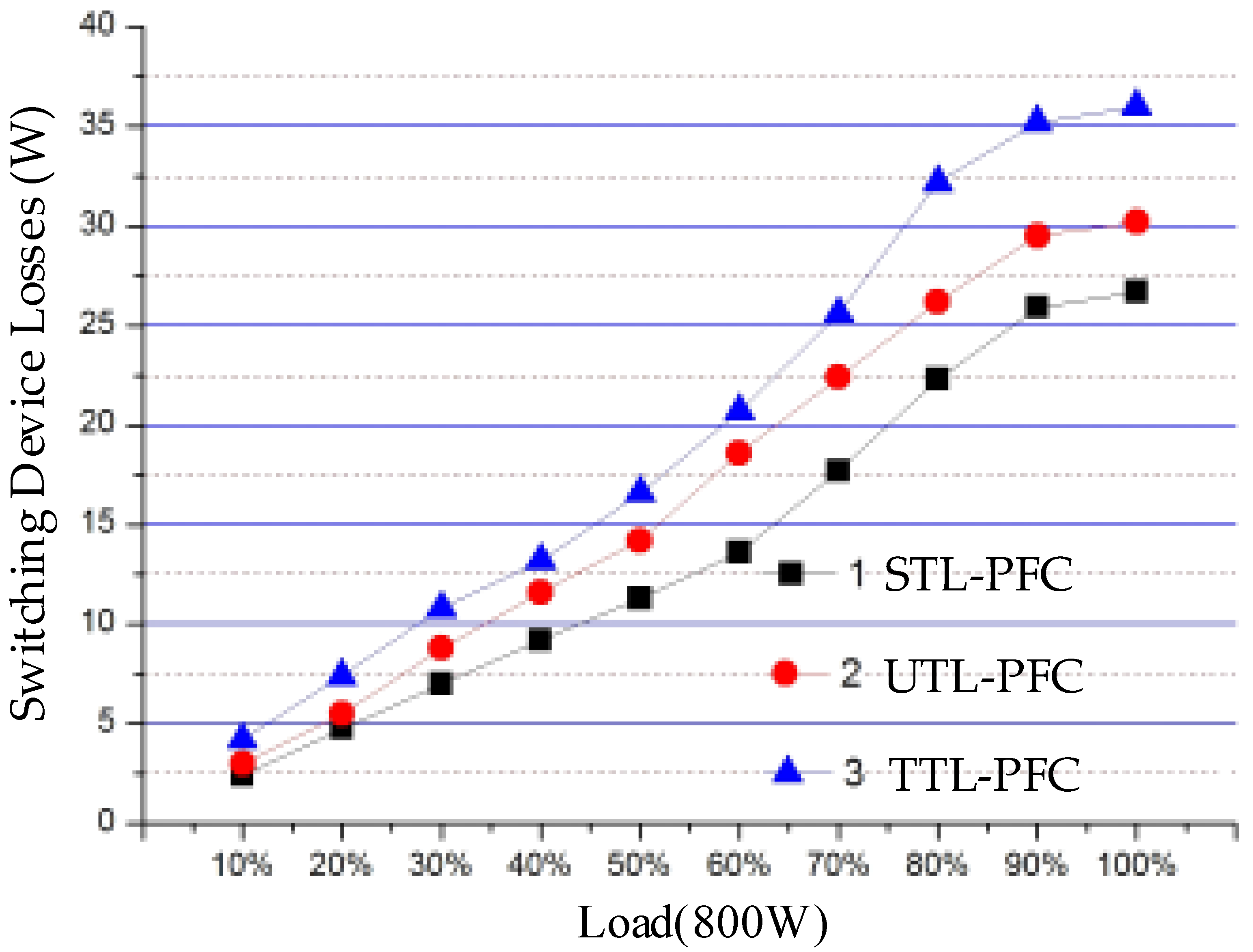
The losses of switching devices have a significant impact on the efficiency of PFC converters, which is mainly composed of the losses of MOSFETs and diodes [21]. Table 3 shows the switching devices in a conduction state in the proposed PFC topologies under different operating modes, where D4 and D6 represent diodes with rated voltages of 400 V and 600 V, respectively. M4 and M6 represent MOSFETs with rated voltage of 400 V and 600 V, respectively. It can be seen from Table 3 that in modes 2 and 5, the STL-PFC has one more diode with a rated voltage of 600 V for conduction than the LATL-PFC and the UATL-PFC, respectively. Hence, the power loss of the STL-PFC is slightly larger than that of the LATL-PFC and the UATL-PFC in the two operating modes. Correspondingly, the number of the conductive switching devices of the STL-PFC, LATL-PFC, and UATL-PFC is the same under other operating modes, so the power losses of the three proposed PFC topologies are similar. In summary, the STL-PFC has the largest power losses among the three proposed PFC topologies.
To verify the validity of the proposed PFC topologies, the representative STL-PFC is selected for loss comparisons with the two typical three-level PFC topologies shown in Figure 1. The specific calculation method of the switching device losses can refer to [22], and the results are shown in Figure 7. It can be seen from Figure 7 that the loss of the STL-PFC is the lowest under different load conditions because, at most, one active switch in each operating mode of the STL-PFC is in a conduction state, further proving that the efficiency of the proposed novel PFC topologies is higher.

4. Multicarrier Modulation Technology Based on Capacitor Voltage Balancing

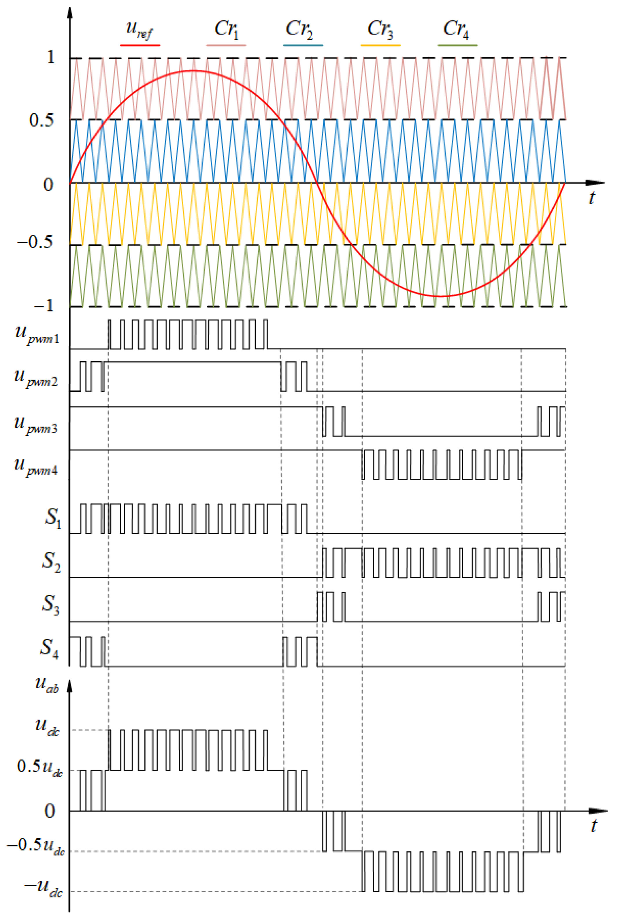
The novel three-level PFC topologies proposed in this paper adopt four-carrier modulation technology to realize pulse signal distribution. As shown in Figure 8, the four equal amplitude and in-phase triangular carriers (Cr1, Cr2, Cr3, and Cr4) are compared with the sinusoidal modulation wave uref. When the value of the modulation wave is larger than that of the carrier, the output PWM signal is high level; otherwise, the output PWM signal is at a low level [23]. According to the comparison, the four PWM waves (upwm1, upwm2, upwm3, and upwm4) can be generated. The pulse signals of the switches (S1~S4) in the proposed PFC topologies can be generated by a logical combination of the four PWM waves (upwm1~upwm4) and the modulation wave uref. The logical relation can be expressed as:
S 1 = u ¯ p w m 1 u p w m 2
S 2 = u ¯ p w m 3 u p w m 4
S 3 = u p w m 3 u p w m 4 1 + sgn ( u r e f ) 2
S 4 = u ¯ p w m 1 u ¯ p w m 2 1 sgn ( u r e f ) 2
where: sgn ( u r e f ) = { 1 ,   if   u r e f > 0   1 ,   if   u r e f < 0 .
In the pulse signal waveforms of the switches S1, S2, S3, and S4, the high-level and the low-level represent the “ON” and “OFF” signals of the switches, respectively. The proposed PFC topologies can operate according to the modes in Table 1 through the mutual cooperation between the pulse signals of each switch, so that the bridge-arm voltage uab can be three-level.
As generally recognized, the phenomenon of unbalanced dc-link capacitor voltage in three-level PFC topologies will increase the voltage stresses of power devices and even lead to device damage in serious cases [24,25,26,27]. Therefore, this problem should be taken into consideration in the control design. Modes 2 and 5 of the proposed novel three-level PFC topologies directly affect the balance of dc-link capacitor voltage. In mode 2, the upper capacitor C1 is charged, and its voltage increases. Meanwhile, the lower capacitor C2 is discharged, and its voltage decreases. However, in mode 5, the voltage fluctuation of the two capacitors is opposite to mode 2. To solve this problem, this paper uses the capacitor voltage balancing method based on multicarrier modulation to achieve the balance of dc-link capacitor voltage. The voltage-current relationship of the capacitor can be expressed as
u c ( t ) = t 0 t 0 + D i T s i ( t ) d t / C i
where i(t) is the charging current of the capacitor, DiTs is the charging time of the capacitor, and Ci (I = 1,2) is the value of the capacitor.
According to (16), the balance of dc-link capacitor voltage can be realized by changing the charging and discharging time of the capacitors, that is, changing the duty cycle Di. Therefore, the modulation wave needs to be modified. This paper uses the PI controller to output the balancing factor α and add it to the original modulation wave to adjust the duty cycle Di. The modified modulation wave can be obtained as
u r e f = α m sin θ
where θ is the reference phase angle of the modulation wave, m is the modulation ratio, and the value range of the balancing factor α is 0.5 < | α | < 1 .
The modified modulation wave can change the operating time of modes 2 and 5 to adjust the charging and discharging time of the upper and lower capacitors, thus realizing the balance of the capacitor voltage.

5. Experimental Validation

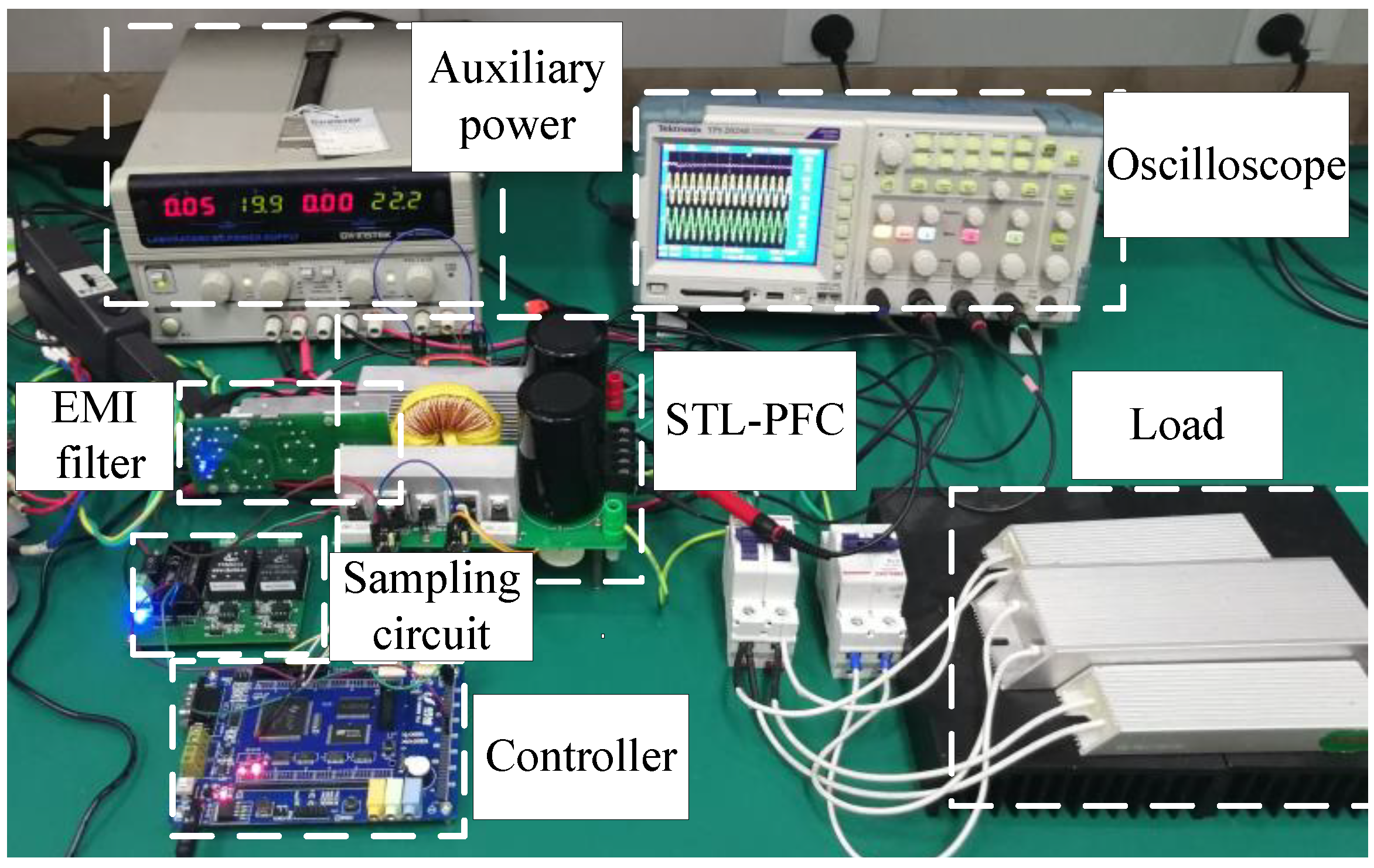
In order to verify the feasibility of the proposed novel three-level PFC topologies, the representative STL-PFC is selected to build the experimental platform, as shown in Figure 9. The main parameters of the experimental circuit are listed in Table 4. The single-phase input AC power is provided by the AC voltage regulator TDGC2-3 kVA, and the controller adopts DSP TMS320F28335. The experimental waveforms are obtained by a Tek-2024B oscilloscope, and the power quality tester adopts E6000.
Figure 10 displays the pulse distribution of the switches S1~S4, which is consistent with the theoretical analysis results, indicating that the proposed topology has the advantage of reducing switching losses.
The experimental results of the STL-PFC operating in a steady state are shown in Figure 11. Here uAC and iL denote the voltage and current of the grid side, respectively, while udc and uab represent the output voltage of the DC side and the bridge-arm voltage, respectively. Additionally, uc1 and uc2 indicate the voltage of the capacitors C1 and C2, respectively. From Figure 11a, the waveform of input voltage uAC is in phase with the waveform of input current iL, meeting the unity power factor. The output DC voltage udc is stable at 400 V, and the peak value of the ripple voltage is 5.3 V. The bridge-arm voltage uab has five voltage levels, which is consistent with the theoretical analysis. From Figure 11b, it can be seen that the voltage waveforms of the two dc-link capacitors maintain dynamic balance, which proves the correctness of the modulation strategy based on capacitor voltage balancing. From Figure 11c, it can be seen that the current harmonic content is 3.99%, which meets the requirement that the harmonic content is less than 5%.
The experimental results of the STL-PFC operating in a dynamic state are shown in Figure 12, where u d c * and ugsp represent the reference of the DC side voltage and the driving voltage signal, respectively.
Figure 12a shows that when the reference voltage u d c * breaks, the DC side voltage udc follows the change and remains at about 500 V, and the input current iL remains sinusoidal after a spike occurs. Still, a large noise interference occurs in the voltage uab due to parameters exceeding design criteria. Figure 12b shows that when the driving signal is lost, the proposed PFC can still work in the uncontrolled rectification state to ensure a reliable power supply for the load. However, a large distortion appears in the voltage uab and the input current iL in this state, and at the same time, the power factor of the proposed PFC is low. Figure 12c shows that when the load changes, the proposed PFC can still achieve power factor correction, and there is only a certain range of small fluctuations in the voltage of the DC side. Figure 12d shows that the voltage waveforms of the upper and lower dc-link capacitors can still maintain good stability when the load increases or decreases by 50%. As the output voltage level increases, the output current will decrease for the same output power, leading to shorter conduction and turn-off times of the switching devices, reducing their switching losses. According to Figure 12e, the efficiency of the STL-PFC also improves. Additionally, the efficiency of the STL-PFC exceeds 97.3%.

6. Conclusions

In this paper, a new family of single-phase, three-level power factor correction (PFC) topologies based on switch-capacitor cells has been presented. The three proposed PFC topologies share the same switching pulse distribution, making utilizing the same modulation method possible. Moreover, these PFC topologies can achieve diode rectification in the event of a switch failure, ensuring a reliable power supply to the load. By limiting the operation to a maximum of one active switch in each mode, the proposed PFC topologies significantly reduce switching losses. The deduction process, operating principle, and circuit characteristics of the PFC topologies have been analyzed in detail, and a suitable modulation technology based on capacitor voltage balancing has been designed. Finally, a laboratory prototype with a rated power of 800 W has been built and tested, with experimental results demonstrating the feasibility and superiority of the proposed PFC topologies.

Author Contributions

Conceptualization, H.M.; Methodology, Y.L. and X.C.; Validation, Y.L.; Data curation, Y.L. and Y.P.; Writing—original draft, H.M.; Writing—review & editing, Y.L., H.M., Y.W., Y.P. and X.C.; Supervision, H.M. and Y.H.; Project administration, Y.H.; Funding acquisition, Y.W., Y.P. and Y.H. All authors have read and agreed to the published version of the manuscript.

Funding

This research was funded by the Hubei Provincial Natural Science Foundation, China grant number [2020CFB248].

Conflicts of Interest

The authors declare no conflict of interest.

References

  1. Chang, C.-H.; Cheng, C.-A.; Chang, E.-C.; Cheng, H.-L.; Yang, B.-E. An Integrated High-Power-Factor Converter with ZVS Transition. IEEE Trans. Power Electron. 2016, 31, 2362–2371. [Google Scholar] [CrossRef]
  2. Singh, S.; Singh, B.; Bhuvaneswari, G.; Bist, V. Power Factor Corrected Zeta Converter Based Improved Power Quality Switched Mode Power Supply. IEEE Trans. Ind. Electron. 2015, 62, 5422–5433. [Google Scholar] [CrossRef]
  3. Amiri, P.; Eberle, W.; Gautam, D.; Botting, C. An Adaptive Method for DC Current Reduction in Totem Pole Power Factor Correction Converters. IEEE Trans. Power Electron. 2021, 36, 11900–11909. [Google Scholar] [CrossRef]
  4. Madishetti, S.; Singh, B.; Bhuvaneswari, G. Three-Level NPC-Inverter-Based SVM-VCIMD With Feedforward Active PFC Rectifier for Enhanced AC Mains Power Quality. IEEE Trans. Ind. Appl. 2016, 52, 1865–1873. [Google Scholar] [CrossRef]
  5. Jang, Y.; Jovanović, M.M.; Kumar, M.; Ruiz, J.M. Three-Level TAIPEI Rectifier—Analysis of Operation, Design Considerations, and Performance Evaluation. IEEE Trans. Power Electron. 2017, 32, 942–956. [Google Scholar] [CrossRef]
  6. Jain, A.; Gupta, K.K.; Jain, S.K.; Bhatnagar, P. A Bidirectional Five-Level Buck PFC Rectifier with Wide Output Range for EV Charging Application. IEEE Trans. Power Electron. 2022, 37, 13439–13455. [Google Scholar] [CrossRef]
  7. Lee, J.-S.; Lee, K.-B. Open-Circuit Fault-Tolerant Control for Outer Switches of Three-Level Rectifiers in Wind Turbine Systems. IEEE Trans. Power Electron. 2016, 31, 3806–3815. [Google Scholar] [CrossRef]
  8. de Souza Kohler, M.A.F.; Cortez, D.F. Single-Phase Five-Level Flying-Capacitor Rectifier Using Three Switches. IEEE Open J. Power Electron. 2020, 1, 383–392. [Google Scholar] [CrossRef]
  9. Ebrahimi, J.; Karshenas, H.; Bakhshai, A. A Five-Level Nested Diode-Clamped Converter for Medium-Voltage Applications. IEEE Trans. Power Electron. 2022, 69, 6471–6483. [Google Scholar] [CrossRef]
  10. Mukherjee, D.; Kastha, D. A Reduced Switch Hybrid Multilevel Unidirectional Rectifier. IEEE Trans. Power Electron. 2019, 34, 2070–2081. [Google Scholar] [CrossRef]
  11. Kim, J.-S.; Lee, S.-H.; Cha, W.-J.; Kwon, B.-H. High-Efficiency Bridgeless Three-Level Power Factor Correction Rectifier. IEEE Trans. Ind. Electron. 2017, 64, 1130–1136. [Google Scholar] [CrossRef]
  12. Vahedi, H.; Shojaei, A.A.; Chandra, A.; Al-Haddad, K. Five-Level Reduced-Switch-Count Boost PFC Rectifier with Multicarrier PWM. IEEE Trans. Ind. Appl. 2016, 52, 4201–4207. [Google Scholar] [CrossRef]
  13. Monteiro, V.; Pinto, J.G.; Meléndez, A.A.N.; Afonso, J.L. A novel single-phase five-level active rectifier for on-board EV battery chargers. In Proceedings of the 2017 IEEE 26th International Symposium on Industrial Electronics (ISIE), Edinburgh, UK, 19–21 June 2017; pp. 582–587. [Google Scholar] [CrossRef] [Green Version]
  14. Rashidi, N.; Wang, Q.; Burgos, R.; Roy, C.; Boroyevich, D. Multi-objective Design and Optimization of Power Electronics Converters with Uncertainty Quantification—Part I: Parametric Uncertainty. IEEE Trans. Power Electron. 2021, 36, 1463–1474. [Google Scholar] [CrossRef]
  15. Zhang, X.; Tan, G.; Liu, Z.; Wang, Q.; Zhang, W.; Xia, T. Finite Control Set Model Predictive Direct Power Control of Single-Phase Three-Level PWM Rectifier Based on Satisfactory Optimization. IEEE Access 2021, 9, 11479–11491. [Google Scholar] [CrossRef]
  16. Mehrabadi, N.R.; Wang, Q.; Burgos, R.; Boroyevich, D. Multi-objective design and optimization of a Vienna rectifier with parametric uncertainty quantification. In Proceedings of the 2017 IEEE 18th Workshop on Control and Modeling for Power Electronics (COMPEL), Stanford, CA, USA, 9–12 July 2017; pp. 1–6. [Google Scholar] [CrossRef]
  17. Zhang, X.; Tan, G.; Xia, T.; Wang, Q.; Wu, X. Optimized Switching Finite Control Set Model Predictive Control of NPC Single-Phase Three-Level Rectifiers. IEEE Trans. Power Electron. 2020, 35, 10097–10108. [Google Scholar] [CrossRef]
  18. Qi, W.; Li, S.; Yuan, H.; Tan, S.C.; Hui, S.Y. High-Power-Density Single-Phase Three-Level Flying-Capacitor Buck PFC Rectifier. IEEE Trans. Power Electron. 2019, 34, 10833–10844. [Google Scholar] [CrossRef]
  19. Lee, M.; Lai, J.S. Fixed-Frequency Hybrid Conduction Mode Control for Three-Level Boost PFC Converter. IEEE Trans. Power Electron. 2021, 36, 8334–8346. [Google Scholar] [CrossRef]
  20. Lee, M.; Kim, J.W.; Lai, J.S. Digital-Based Critical Conduction Mode Control for Three-Level Boost PFC Converter. IEEE Trans. Power Electron. 2020, 35, 7689–7701. [Google Scholar] [CrossRef]
  21. Najjar, M.; Kouchaki, A.; Nielsen, J.; Lazar, R.D.; Nymand, M. Design Procedure and Efficiency Analysis of a 99.3% Efficient 10 kW Three-Phase Three-Level Hybrid GaN/Si Active Neutral Point Clamped Converter. IEEE Trans. Power Electron. 2022, 37, 6698–6710. [Google Scholar] [CrossRef]
  22. Zhang, L.; Sun, K.; Xing, Y.; Zhao, J. A Family of Five-Level Dual-Buck Full-Bridge Inverters for Grid-Tied Applications. IEEE Trans. Power Electron. 2016, 31, 7029–7042. [Google Scholar] [CrossRef]
  23. Iqbal, A.; Meraj, M.; Tariq, M.; Lodi, K.A.; Maswood, A.I.; Rahman, S. Experimental Investigation and Comparative Evaluation of Standard Level Shifted Multi-Carrier Modulation Schemes with a Constraint GA Based SHE Techniques for a Seven-Level PUC Inverter. IEEE Access 2019, 7, 100605–100617. [Google Scholar] [CrossRef]
  24. He, X.; Yu, H.; Han, P.; Zhao, Z.; Peng, X.; Shu, Z.; Koh, L.; Wang, P. Fixed and Smooth-Switch-Sequence Modulation for Voltage Balancing Based on Single-Phase Three-Level Neutral-Point-Clamped Cascaded Rectifier. IEEE Trans. Ind. Electron. 2020, 56, 3889–3903. [Google Scholar] [CrossRef]
  25. Zhang, P.; Wu, X.; Chen, Z.; Xu, W.; Liu, J.; Qi, J. A Multizero-Sequence Component Injection Algorithm for a Five-Level Flying Capacitor Rectifier Under Unbalanced DC-Link Voltages. IEEE Trans. Power Electron. 2021, 36, 11967–11983. [Google Scholar] [CrossRef]
  26. de Freitas, I.S.; Bandeira, M.M.; de Macedo Barros, L.; Jacobina, C.B.; dos Santos, E.C.; Salvadori, F.; da Silva, S.A. A Carrier-Based PWM Technique for Capacitor Voltage Balancing of Single-Phase Three-Level Neutral-Point-Clamped Converters. IEEE Trans. Ind. Appl. 2015, 51, 3227–3235. [Google Scholar] [CrossRef]
  27. Dargahi, V.; Sadigh, A.K.; Khorasani, R.R.; Rodriguez, J. Active Voltage Balancing Control of a Seven-Level Hybrid Multilevel Converter Topology. IEEE Trans. Ind. Electron. 2022, 69, 74–89. [Google Scholar] [CrossRef]
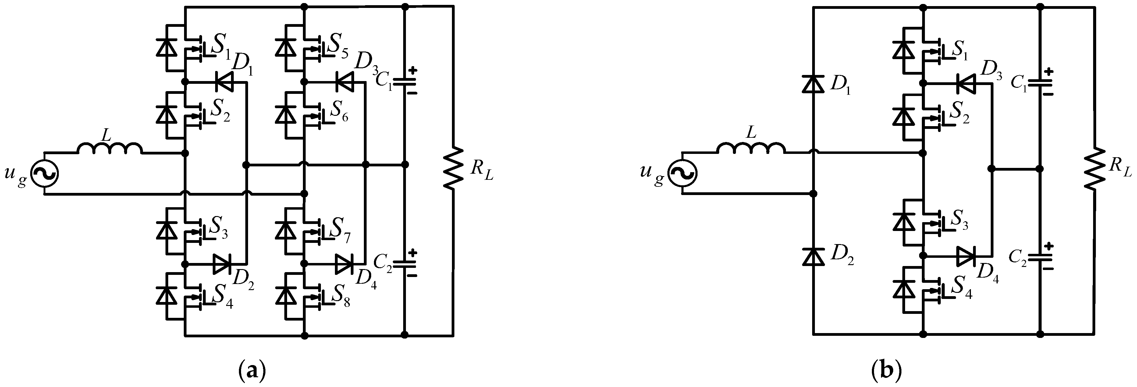
Figure 1. Two typical single-phase three-level PFC topologies. (a) TTL-PFC. (b) UTL-PFC.
Electronics 12 01286 g001
Figure 2. Two forms of the switch-capacitor cell. (a) common anode SCC. (b) common cathode SCC.
Electronics 12 01286 g002
Figure 3. Three novel single-phase three-level PFC. (a) STL-PFC. (b) UATL-PFC. (c) LATL-PFC.
Electronics 12 01286 g003
Figure 4. Current paths corresponding to six operating modes of the STL-PFC: (a) Mode 1 (iL > 0, uab = +0); (b) Mode 2 (iL > 0, uab = +0.5udc); (c) Mode 3 (iL > 0, uab = +udc); (d) Mode 4 (iL < 0, uab = −0); (e) Mode 5 (iL < 0, uab = −0.5udc); (f) Mode 6 (iL < 0, uab = −udc).
Electronics 12 01286 g004
Figure 5. Key operating waveforms of the STL-PFC in theory.
Electronics 12 01286 g005
Figure 6. The equivalent circuit model of the STL-PFC topology.
Electronics 12 01286 g006
Figure 7. Switching device losses of three PFC topologies under different load conditions.
Electronics 12 01286 g007
Figure 8. The pulse width modulation principle of the proposed PFC.
Electronics 12 01286 g008
Figure 9. Experimental prototype platform.
Electronics 12 01286 g009
Figure 10. The pulse distribution waveforms of four switches in the STL-PFC.
Electronics 12 01286 g010
Figure 11. The experimental results in a steady state. (a) The DC output voltage udc, the input voltage vAC, the inductor current iL, and the bridge-arm voltage uab. (b) The capacitor voltage uc1, uc2. (c) Analysis of harmonic content.
Electronics 12 01286 g011
Figure 12. The experimental results in a dynamic state. (a) Experimental waveforms during the reference voltage increase from 400 V to 500 V. (b) Experimental waveforms from uncontrolled process jump to controllable process. (c) Experimental waveforms when the load increases or decreases by 50%. (d) The capacitor voltage waveforms when the load increases or decreases by 50%. (e) Efficiency comparison at different output voltage levels.
Electronics 12 01286 g012
Table 1. Switching states and system parameters.
ModesSwitching StatesSystem Parameters
S 1 S 2 S 3 S 4 i + i i s 1 i s 2 i s 3 i s 4 u a b u c 1 u c 2
i L > 0 1000100000 i L 0
210000 i L i L 0 i L 0 u c 2
30000 i L i L 00 i L 0 u c 1 + u c 2
i L < 0 400100000 i L 00
50100 i L 00 i L 0 i L u c 1
60000 i L i L 000 i L u c 1 u c 2
Table 2. Maximum voltage stresses of the switching devices in the proposed topologies.
Switching DevicesSTL-PFCUATL-PFCLATL-PFC
S10.5udc0.5udc0.5udc
S20.5udc0.5udc0.5udc
S3udcudcudc
S4udcudcudc
D1, D2udcudcudc
D3, D40.5udc0.5udc0.5udc
D5, D6udcudcudc
Table 3. Switching devices in conduction state under different operation modes.
Operating
Modes
Devices(Number × Rated Voltage)Voltage u a b
STL-PFCUATL-PFCLATC-PFC
Mode 11 × D6,1 × M61 × D6,1 × M61 × D6,1 × M6+0
Mode 21 × D4,3 × D6,1 × M41 × D4,3 × D6,1 × M41 × D4,2 × D6,1 × M4+0.5udc
Mode 34 × D64 × D64 × D6+udc
Mode 41 × D6,1 × M61 × D6,1 × M61 × D6,1 × M60
Mode 51 × D4,3 × D6,1 × M41 × D4,2 × D6,1 × M41 × D4,3 × D6,1 × M4−0.5udc
Mode 64 × D64 × D64 × D6udc
Table 4. Main Parameters of The Experimental Circuit.
DescriptionLabelValue
Input voltageuAC220 Vrms
Output rated voltageudc400 V
Rated output powerPo800 W
Switching frequencyf50 kHz
InductorL2 mH
CapacitorC1/C21000 μF
MOSFETsS1~S4STW26NM60N
DiodesD1~D6RHPR3060
Disclaimer/Publisher’s Note: The statements, opinions and data contained in all publications are solely those of the individual author(s) and contributor(s) and not of MDPI and/or the editor(s). MDPI and/or the editor(s) disclaim responsibility for any injury to people or property resulting from any ideas, methods, instructions or products referred to in the content.