1. Introduction
The rapid development of new communication standards, resulting in the need for rapid prototyping and testing of new radio devices, led to the widespread use of radio systems based on the relatively new concept of Software-Defined Radio (SDR). This technology owes its undeniable potential to an effective homodyne: zero intermediate frequency (ZIF) architecture with quadrature signal processing in digital, reprogrammable baseband [
1,
2]. Unlike the classic heterodyne (non-zero IF) system with a standard-oriented and strictly defined hardware structure, the SDR approach enables the analogue radio hardware to be reduced. This way, the financial outlays related to hardware prototyping, production, maintenance, and modification of the system are lowered. Besides the costs, it makes systems more versatile and flexible owing to the ability to support multistandard operations in the broadest possible frequency range. At the same time, the system’s required functionality is defined almost only at the level of standard-specific interchangeable software [
3,
4] and the hardware parameters used. The constraints here are A/D and D/A conversion capabilities and the frequency tunability of the RF front-end.
Technological progress in integrated circuits (IC) for SDR systems is so fast that there are no significant publications presenting characteristics or performance comparisons of available integrated transceivers. The second reason for the low number of scientific papers is industrial secrecy, i.e., keeping the results of the research and development activities a secret from the competitors. As a consequence, an expert discussion suffers from a lack of information and experience exchange. In practice, the development of new SDR devices is based on documentation such as datasheets, application notes, etc., and on the designers’ experience gained in the past from prototyping the appliances built with previous generations of ICs recommended for SDR applications.
Generally, modern radios [
5] have a modular structure composed of two main blocks: an SDR platform including a digital signal processor (DSP) for baseband processing and a dedicated RF front-end. In many cases, such as in multiple-input multiple-output (MIMO) systems, the RF front-end has two or more identical RF channels, each consisting of a transmit and receive signal path. Typical functional blocks, which can be found in an RF channel, are a filter, duplexer or switch, limiter, power amplifier (PA), and low noise amplifier (LNA). In some solutions, it may comprise an additional frequency conversion stage. Though the RF front-end contains many of the components mentioned above necessary for the operation of a whole system, it is increasingly treated as a peripheral (supporting) block to the SDR platform. Its main task is to match an antenna to a ZIF transceiver in terms of gain and frequency and keep a high linearity and selectivity of processing, a low noise floor, and appropriate amplification to drive successive stages correctly or protect against overdriving.
With the reduced receive and transmit paths, direct analogue conversion to baseband A/C and C/A converters, and digital processing, the SDR platform is a central part of the modern radio system. The SDR platform and a baseband processor create a frequency and functionality-independent hardware framework. Its operation may be defined only by the operating frequency range and processing bandwidth.
The modular structure of the hardware platform presented in this paper provides a high level of reconfigurability. It allows for quick testing of a complete radio link and signal processing algorithms, for example, a custom implementation of the crest factor reduction (CFR) or digital predistortion (DPD) algorithm. The platform can also be used for evaluation of some hardware components, such as power amplifiers optimized for maximal linearity.
SDR platforms are commonly considered in the literature as profiled tools designed for specific applications or research in areas such as cellular communication [
6,
7,
8,
9], radar technology [
10], IoT [
11,
12,
13], education [
14], radio transmission security/pentesting [
15,
16], space communication [
17,
18], cognitive radio [
19], SigInt [
20], jamming [
21], spoofing [
22], and the application of deep learning in various fields using RF signals [
23,
24]. Thus, off-the-shelf SDR hardware interfaces are usually used for these tests. Only a few publications report the current technology level of SDR platforms used to build modern RF systems, with exemplary solutions focused more on hardware than functionality [
25,
26].
As mentioned above, the literature on the subject is relatively poor. Therefore, the paper aims to fill this gap, especially in designing universal platforms to accelerate and facilitate the prototyping of micro base stations or remote radio units (BTS, eNodeB, RRU—depending on the standard being considered). The motivation for the design effort presented in this paper was a rapidly growing interest in private (nonpublic) LTE and 5G networks, which are expected to find several applications in highly automated industrial environments [
27,
28].
In the paper, we have focused on the following issues:
A universal hardware framework we have developed for designing novel LTE-A micro base stations and scientific experiments, with a top-level view presented in
Section 2 and more detailed description in
Section 4;
A brief overview of available SDR transceivers and their development roadmaps (
Section 3);
Exemplary applications, including construction details (block diagrams, selected electronic components) of RF front-ends for two popular LTE B43 and B31 bands (
Section 5) that we designed;
2. The General Concept of the Universal Hardware Platform
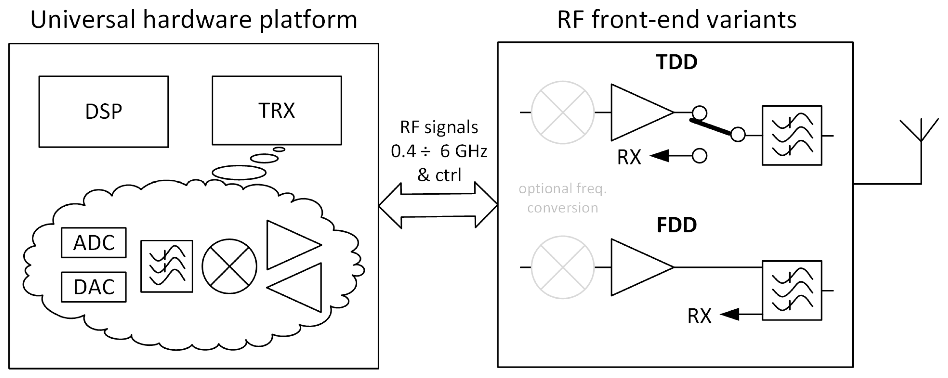
A universal platform for modern radio prototyping should have high flexibility and versatility to test various system solutions and apply many debugging schemes with capturing and injecting internally processed digital signals. To meet these expectations, we have proposed a Universal Hardware Platform (UHP) with the architecture shown in
Figure 1.
As shown in
Figure 1, the UHP consists of an integrated SDR transceiver (TRX) cooperating with a baseband processor (DSP). The RF front-end is here considered an attachable component that may be replaced according to the desired configuration. Its main task is to adapt the system to specific requirements defined by the application scenario. Due to TRX limitations in its vast RF band, such as low output power level or high noise figure, the RF front-end ultimately shapes the system performance, i.e., a working sub-band from the TRX frequency range, gain adjustment range of the receiving path (RX), noise figure, maximum power, and an acceptable nonlinear distortion level at the output of the transmitting path (TX).
The RF front-end carries out a duplex scheme specified by the standard for time division duplex mode (TDD) using a switch or for frequency division duplex (FDD) with a duplexer. Optionally, an additional classical up- or down-converter can be used to expand a system’s operating frequency range below or above the band supported by a transceiver.
3. Integrated Transceiver Overview
As noted above, the transceiver is the SDR platform’s crucial element responsible for the signal transition between analogue and digital forms in both directions. In the early days of the SDR technology, transceivers were built with highly specialized ICs, such as IQ (de)modulators, frequency synthesizers, amplifiers, ADCs and DACs. Examples of SDR hardware are educational platforms, such as the popular ones from Ettus (N series) [
29], devices developed by the authors of this paper [
30,
31], and arbitrary generators or vector analyzers in professional RF laboratory. They all feature a native modular structure. This approach to designing SDR platforms limited the possibilities of spatial miniaturization and required increased care in routing analogue signals in their quadrature form.
An effective way to improve the performance of transceivers and SDR platforms is an integration of most of their components into a single chip, which is how it is done now. Today, the transceiver is a highly integrated monolithic circuit comprising independent multichannel receivers and transmitters, PLL synthesizers, a high-speed serial interface, and built-in digital signal processing functions. The first integrated transceiver containing the key components mentioned above was launched by Lime Microsystems in 2011, more than a decade ago [
32]. The competitive ICs of the AD936X series from Analog Devices appeared shortly after [
33]. Integrated TRX circuits made it possible to design radio systems that complied with the standards of the time.
A few years later, there was an increase in bandwidth in the next generation of transceivers, understood as the width of the simultaneous bandwidth of the signal delivered by the transmitter and the carrier frequency tuning range. The insufficient sideband product suppression and LO leakage, which was a limitation in the case of the first TRX generation, was improved. More functionalities were introduced, such as AGC, programmable filters, and mechanisms performing build-in or custom linearization of transmitting paths. Channels were multiplexed to build MIMO systems. The third TRX generation, currently under development, aims to expand the bandwidth of synthesized signals further to meet the requirements of multicomponent systems in 5G new radios and deploys functionalities specified by existing standards, such as CFR. Attempts are also made to replace the analogue frequency conversion with direct sampling architecture using ultrafast A/D and D/A converters [
34].
An overview of the currently available integrated transceivers for SDR systems is contained in
Table 1. The best-performing models in each IC series were selected based on the number of RF channels and built-in functionalities.
In the early stage of development, the miniaturization of ZIF architecture systems with preintegrated transceivers came at a price. Such effects as the quadrature imbalance, distortions around the center frequency of the processed channel, and carrier leakage were especially troublesome. They are all known from analogue implementations of IQ modulators and demodulators [
3,
39]. The above effects and processing linearity had to be corrected to provide proper operation and satisfactory radio performance. To do that, additional treatments during digital signal processing are required. Today’s second- and third-generation SDR transceivers usually have built-in linearization, calibration, and correction mechanisms operating on the fly.
The third generation transceivers recommended mainly for SDR systems have already been deployed. This fact proves that SDR technology has been widely adopted in radio devices and is constantly being improved. Indeed, with its participation, the rapid development of new standards occurs.
To summarize, the currently available TRX ICs allow for designing radio systems with a carrier frequency range of up to 6 GHz and a simultaneous transmission bandwidth of up to 1000 MHz, typically 100 MHz [
40].
4. Universal Hardware Platform
4.1. Top-Level Block Diagram of Universal Hardware Platform
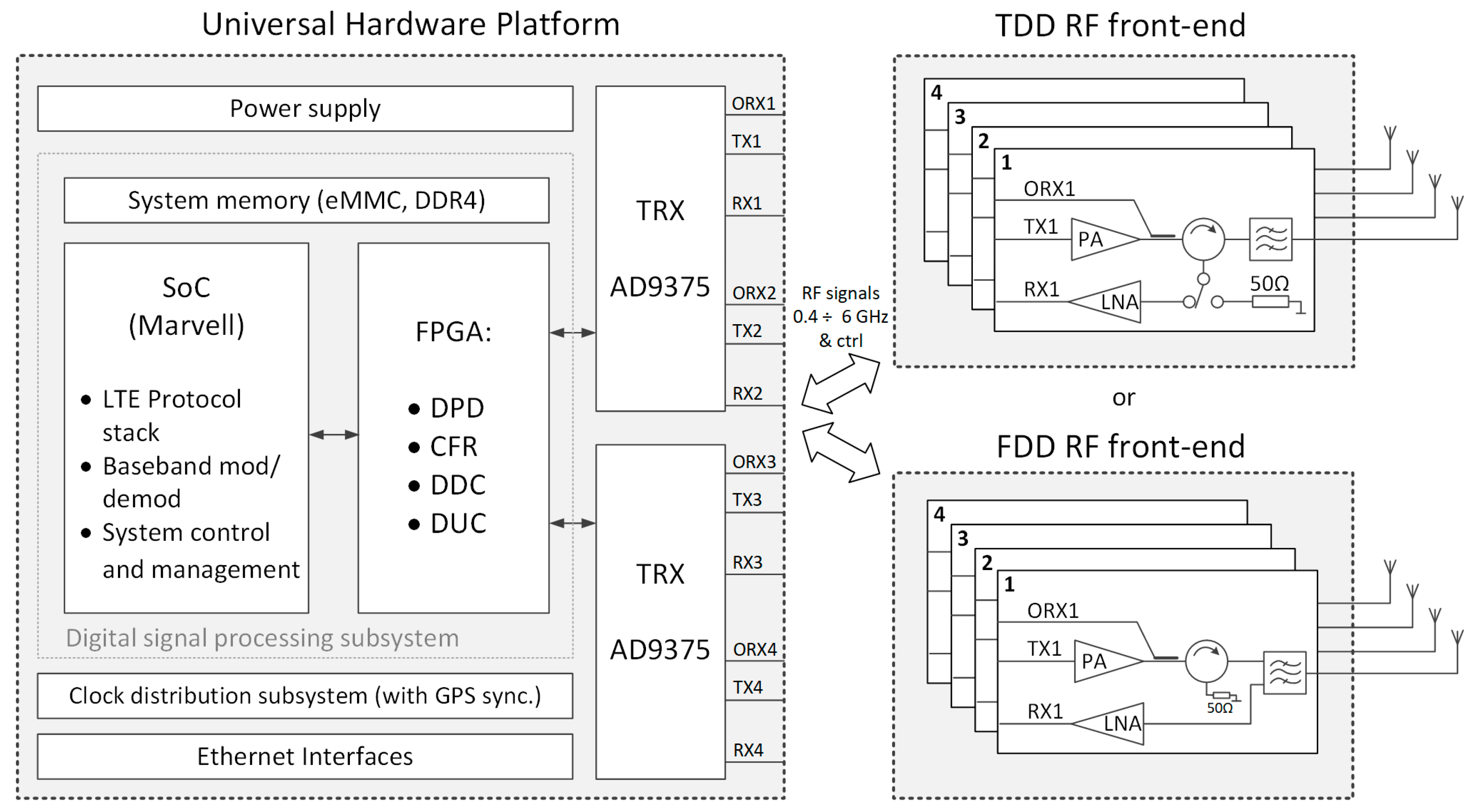
Two postulates determined the final choice of the UHP hardware solution: the need for versatility and an extended use time. Hence, we focused on the fourth-generation cellular systems (namely: LTE-Advanced), considering carrier aggregation and multichannel transmission up to 4 × 4 MIMO. This led to the requirement of 100 MHz instantaneous synthesis bandwidth with the possibility of observation and correction of the transmitted signals in the band up to 250 MHz. The carrier frequency needs to be tunable in a 300 MHz to 6000 MHz frequency range. Additionally, both duplex schemes (FDD and TDD) need to be implementable. Our proposal for the Universal Hardware Platform architecture is shown in
Figure 2 as a block diagram.
4.2. Integrated ZIF Transceiver
In order to enable us to implement MIMO systems, the proposed platform had to have at least four complete (Tx and Rx) channels. Therefore, two highly integrated RF transceivers AD9375 from Analog Devices were employed to build the UHP. At the time of selection, the AD9375 provided an optimal trade-off between the integration level, cost, and RF performance [
36]. The AD9375 incorporates two complete transmit and receive channels equipped with signal leveling, an observation receiver to monitor the transmitter output signal, and a single direct frequency conversion block with A/D and D/A converters. The TRX chip also performs some functions of digital signal preprocessing, i.e., filtering, correction of analogue quadrature processing effects, support for FDD or TDD modes, and linearization by means of the DPD. The AD9375 transceiver specification is highlighted in
Table 1.
4.3. Digital Signal Processing Subsystem
The digital signal representation of RF signals acquired or synthesized by the transceivers (AD9375) is processed in the digital signal processing subsystem. From the hardware point of view, it is a hybrid in which two major component classes can be distinguished:
A standard-specific system-on-chip (SoC) that performs all low-level operations on the individual LTE Component Carriers, including synchronization, equalization, (de)modulation, (de)coding, correction, and also resource scheduling and user data exchange with other networks through a wired interface,
FPGA coprocessor that provides high-level flexibility in prototyping and debugging filters, digital up/down-conversion (DUC, DDC), CFR, and DPD algorithms.
Among several SoCs available on the market [
41,
42,
43], an IC from the Octeon Fusion-M CNF73xx family [
44] was used. The Marvell CNF73xx stands out by many hardware accelerators and CPU cores, enabling simultaneous processing of the LTE protocol stack. The Marvell IC performs baseband synthesis and demodulation up to 8 LTE Component Carriers (CC), each 20 MHz width, or up to 16 CC at a lower bandwidth. Relatively high computing power translates directly into the number of supported network cells and simultaneously supported terminals. The manufacturer’s technical support level and software development kit (SDK) availability were rigorous criteria for choosing the SoC.
Selection of FPGA for the coprocessor involved analysis of several parameters such as the number of DSP blocks, number of configurable logic blocks, and amount of embedded memory. An important factor was the number of high-speed transceivers necessary for data exchange between SoC, FPGAs, and TRXes. Finally, due to the price-to-performance ratio, two Xilinx Artix family chips were used as coprocessors.
For correct operation of the entire platform, a few more components were needed. They were as follows: a wired network interface (copper and optical fiber), DDR memory banks, a GPS-disciplined precise clock source with a suitable distribution over all crucial subsystems, a supervision microcontroller, switched-mode power supplies for SoC and transceivers, and TX/RX switching logic sequencers.
4.4. RF Front-End
The UHP can be employed to develop a system capable of operating in the frequency range from 400 MHz to 6 GHz in TDD or FDD mode with a simultaneous bandwidth of up to 100 MHz. The operating RF frequency range may be shifted toward higher bands with additional frequency conversion. Note that the analysis bandwidth for the observation receiver (ORX) and synthesis in the TX path equals 250 MHz. Such a bandwidth meets the requirements of the linearization process as the analysis bandwidth must be broader than the one the transmission channel occupies.
Though the UHP reconfiguration for the selected radio standard is performed by baseband processor reprogramming, the RF front-end may also be replaced if necessary. According to the paradigm of the SDR-based system, a primary front-end function is to optimally level the signal in both the receive and transmit directions while keeping distortions low enough. The transmitting radio path design guidelines are specified in detail below:
High-efficiency PA that accounts for a substantial contribution of the overall power consumption is, thus, crucial for thermal management;
A 20 dB range of the output power control for the signal that is a sum of four 20 MHz E-UTRA components distributed in the band up to 100 MHz (according to LTE specification [
6]);
SWR monitoring to mitigate the consequences of an accidental antenna system malfunction;
PA protection against overheating due to a random overdrive of PA by improperly leveled signal or CW excitation, which may happen in systems operating with a high peak-to-average power ratio (PAPR);
Fulfillment of EM compatibility guidelines using proper shielding to reduce crosstalk that can generate severe problems in FDD systems.
The main recommendations for receiving channels are as follows:
Providing an appropriate gain budget, low noise figure and interference robustness;
Ensuring selectivity in the frequency domain;
Gain control in the receive path;
Protection of the monolithic transceiver against high-power destructive signals.
An RF front-end designed correctly in terms of electrical and mechanical requirements should meet the above guidelines. In the case of the transmit path, it comes down to the design of a high-efficiency, high-power amplifier with effective heat dissipation to the base station housing. The tracking functionalities in the TX path should control power output, monitor the reflected power from the antenna, and protect the PA against clipping. The crucial task is to correct and monitor nonlinear distortions at the amplifier output through the DPD algorithm.
The receiving path comprises a low-noise amplifier (LNA) with a sufficiently high gain, low noise figure, a proper output power level at 1 dB gain compression point, and high linearity expressed by high IP3. The receiver should be protected against too large signals using either a diode limiter or a robust GaN-based amplifier acting as LNA. Out-of-band signals also need to be filtered.
4.5. RF Duplexing, Self-Management, and Diagnostics
The RF front-end board is equipped with a supervisor microcontroller (PSoC 5LP family), which sets proper timings for TX/RX switching sequences and maintains the safe operation of PA and LNA. Each TX path is continuously monitored by forward and reflected power detectors necessary to measure the antenna SWR and the peak power at the TX output, respectively. Although PAs are designed to operate with OFDM signals, one should protect them against overdriving, which could happen when the amplifier starts up or tests. This protection is achieved with envelope detectors, comparators, and timeout counters, which disable a particular amplifier if only the power level exceeds the threshold for a predefined time (e.g., approx. 100 µs).
5. Designs and Results
This section focuses on the technical solutions used in the UHP and two developed RF front-ends capable of TDD and FDD operation in the LTE B43 and B31 bands, respectively.
5.1. Universal Hardware Platform for LTE Micro Base Station
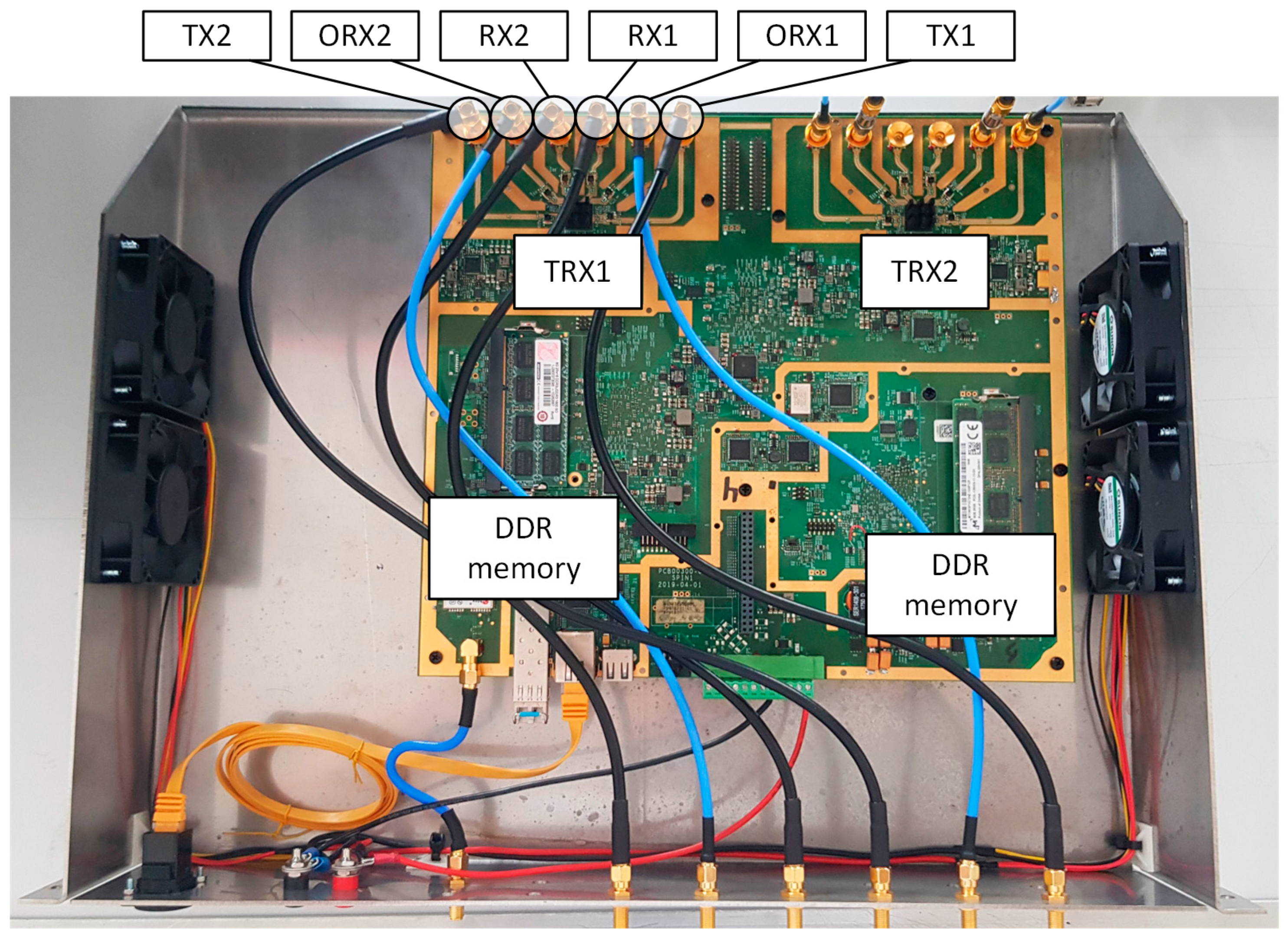
The test fixture built with UHP is shown in
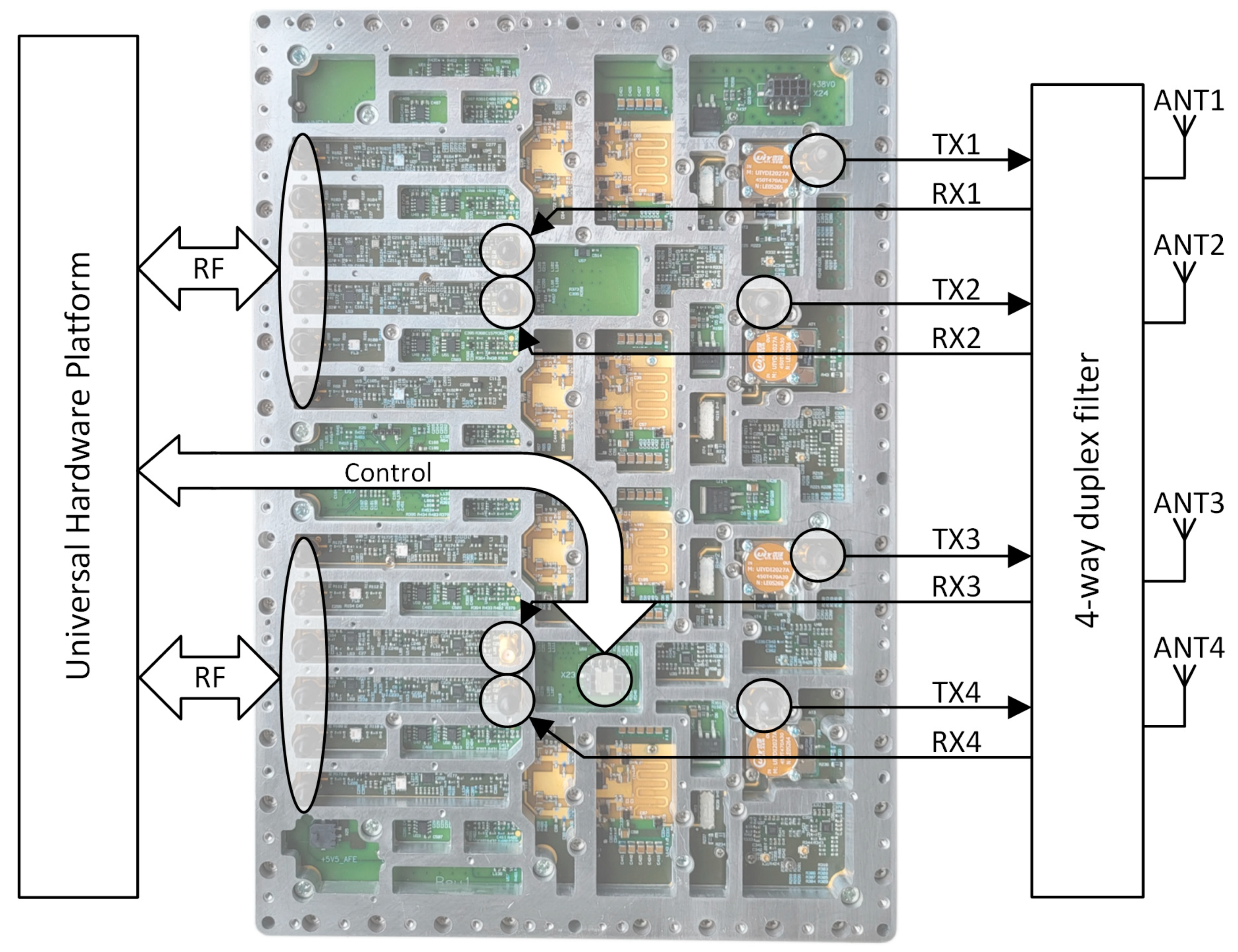
Figure 3. The UHP printed circuit board was made on a 12-layer Megtron-6 substrate. The three main components of the digital signal path (the Marvell SoC for LTE signals baseband processing and two Artix-family FPGAs) are mounted on the bottom side. In addition to them, the board is equipped with the GPS-disciplined global clock distribution circuit, external connectivity interfaces (SFP connector, 1 GbE Ethernet, USB), essential switched-mode power regulators, and the supervisory MCU. RF signals are exchanged between SDR transceivers and the RF front-end via a row of twelve PSMP connectors. They serve connectivity in two ways: cable-based or compact board-to-board integration with a help of tiny female-to-female PSMP bullets. The second way is crucial for transforming the set-up into a compact LTE micro base station fitted into a waterproof, passively cooled metal case, which can be installed on a remote site and serve LTE signals over the air for practical field tests.
Two DDR memory modules are used for debugging purposes to enable capturing signal chunks for further off-line diagnostics with external, custom-designed Python-based tools. Moreover, an inverse operation is available, i.e., a test signal can be synthesized externally, uploaded to the DDR memory, and injected into a selected point in the digital signal path. Although this method does not offer real-time streaming, it is instrumental in troubleshooting and implementing digital connectivity between SoC, FPGAs and TRXs, DUC, DDC, digital filters, CFR and DPD algorithms. The chunk-based processing significantly relaxes requirements for computing resources and data storage with a minimal loss of functionality. The debugging subsystem can be bypassed. In this situation, the SoC and FPGA-implemented coprocessor performs the signal processing, providing real-time operation as an LTE micro base station.
5.2. LTE RF Front-End Design
According to the design guidelines above, two RF front-ends have been developed. The one for LTE B43 band carries out connectivity within the 3.6 ÷ 3.8 GHz frequency range in the time duplex mode TDD through four RF channels with more than 10 watts of average power per channel. It is equipped with a supervisory MCU, which provides internal diagnostics, safety measures, and easy interfacing with the rest of the system. The second one allows for the four-channel LTE-A B31 band transmission in FDD mode with an average output power of over 1 W per each channel.
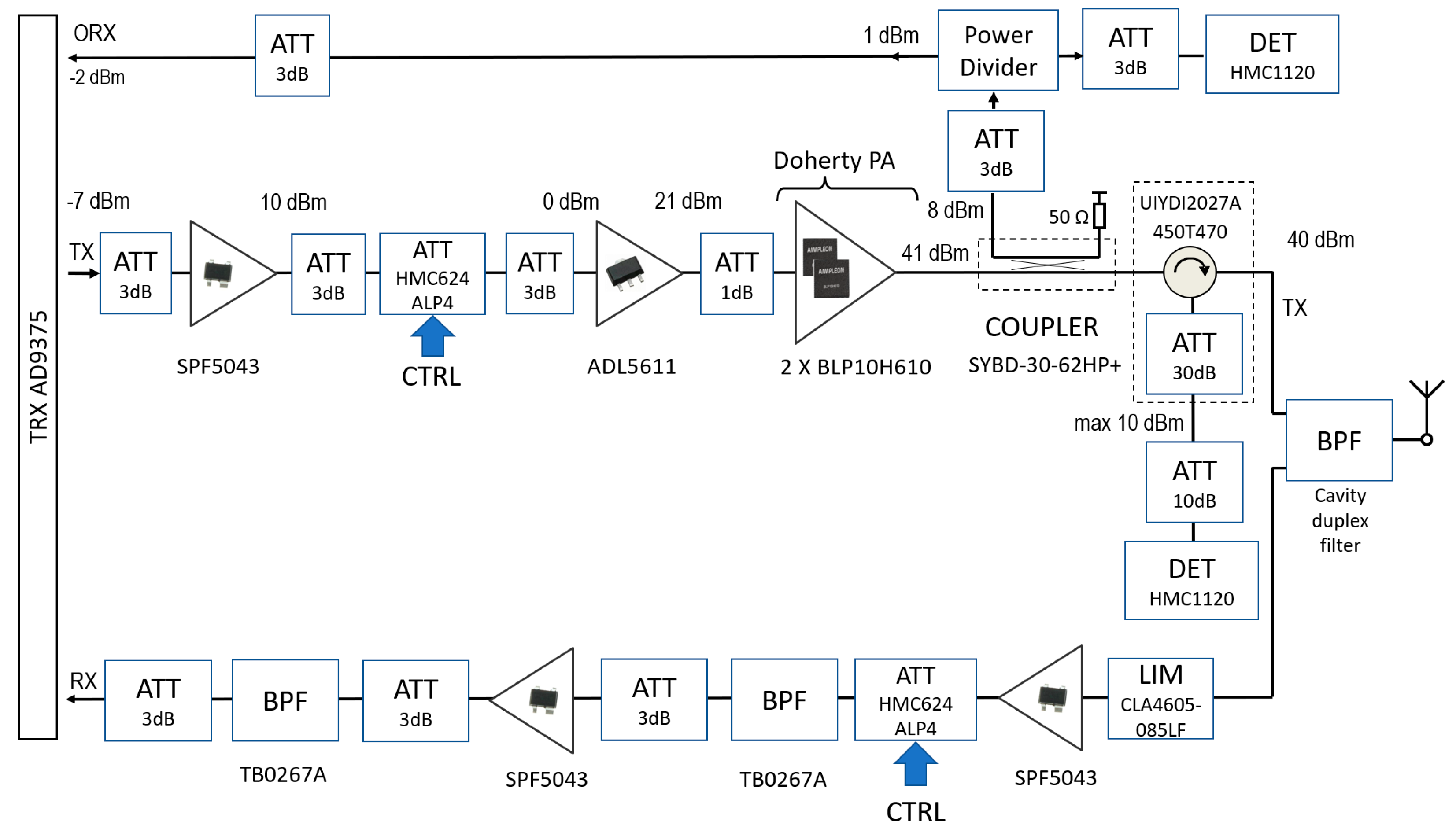
5.2.1. B43 RF Front-End
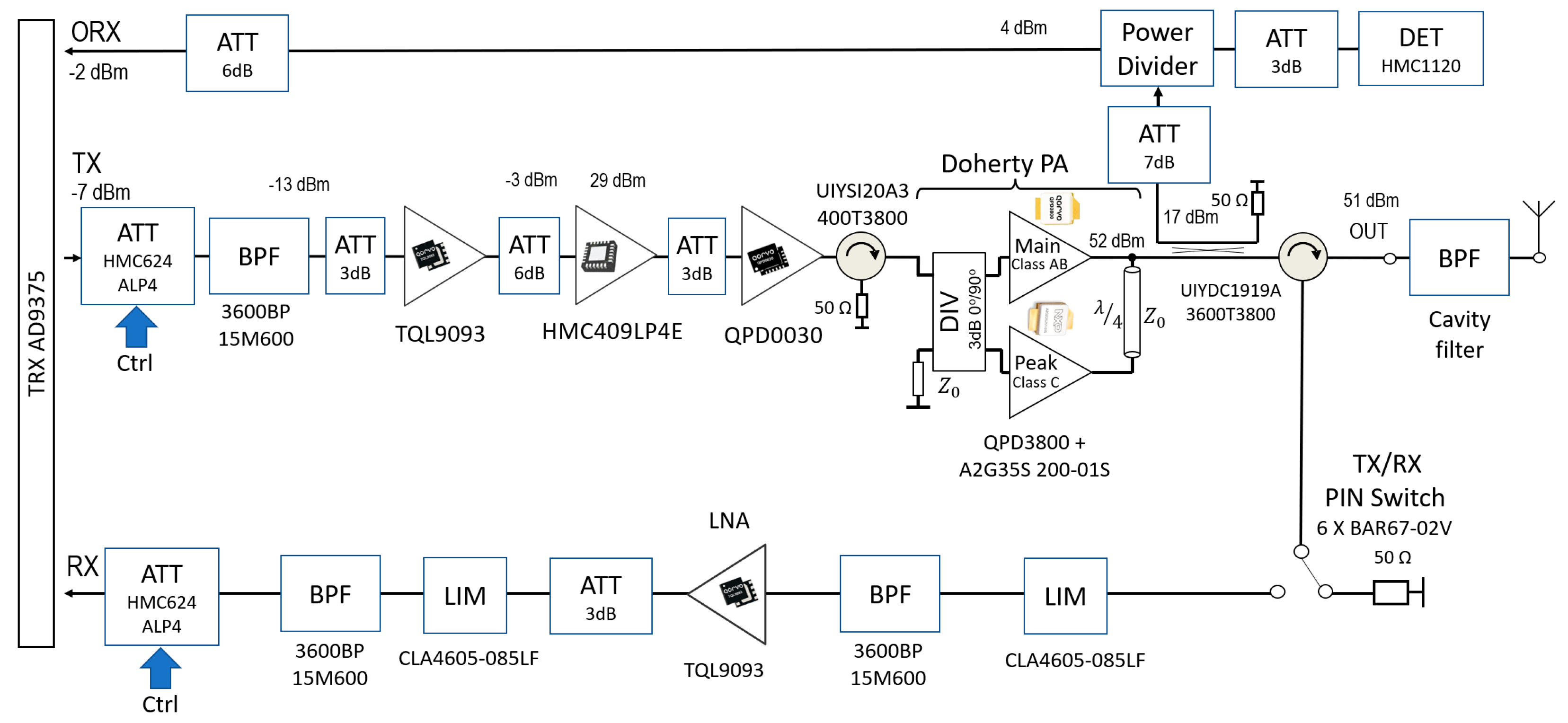
Each RF channel of the front-end has the same structure. The single RF channel block diagram is shown in
Figure 4. The antenna routing between TX and RX radio paths for the TDD RF front-end is carried out in a passive manner by means of an RF circulator, supported by a custom-designed PIN-diode switch. The circulator can unidirectionally conduct a high-power signal with low distortion and loss. At the same time, a PIN switch connects the third circulator port to either a dummy load or RX input. The switch was designed using six PIN diodes BAR67-02V (Infineon). Therefore, many diodes were needed to obtain the proper isolation of more than 30 dB between the switch ports.
As shown in
Figure 4, the receive path contains a limiter (LIM), bandpass filter (BPF), low noise amplifier (LNA), second limiter and BPF, and a digitally controlled attenuator. A limiter protects the LNA against overdriving and, finally, from destruction. It was made with PIN limiting diodes CLA4605-085LF from Skyworks Solutions (Irvine, CA, USA). The limiter achieved a 1 dB threshold level for the input power equal to 10 dBm and output leakage of 16 dBm for 35 dBm maximal input power within band B43. The bandpass filter BPF 3600BP15M600 (Johanson Technology (Camarillo, CA, USA)) was used to limit the band of LNA input signals to the frequency range B43. Even though BPF is a surface-mount device with a small size (2 mm × 2 mm), it exhibits a low insertion loss of 1.6 dB in-band and high attenuation out-band.
As the LNA, the monolithic amplifier TQL9093 by Qorvo (Greensboro, NC, USA) is used. It is optimized for noise figure less than 0.8 dB at the 20 dB gain and high output power (P1dB) at the 1 dB gain compression point over a 1.5 GHz to 4 GHz frequency range. In addition, the TQL9093 features a low supply voltage from 3.3 V to 5 V and high robustness for RF input power up to 27 dBm. It is also equipped with a shut-down control pin driven by 1.8 V TTL logic. The aforementioned features make this particular chip highly suitable for operating in a TDD system, such as this RF front-end is designed for. A second limiter, the same as the previous one, is located between the LNA and the next bandpass filter BPF and assures appropriate signal levels and protects the transceiver chip. A GaAs 6-bit digital attenuator HMC HMC624ALP4 (Analog Devices (Wilmington, MA, USA)) with a 30 dB attenuation control range in a 0.5 dB step is the last component before the TRX AD9375 described in the previous section.
The signal In the TX radio path is leveled by a digitally controlled attenuator HMC HMC624ALP4 (ADI), filtered with the BPF 3600BP15M600, and then amplified by a four-stage power amplifier (PA) to the desired power level. The PA consists of a two-stage preamplifier, driver, and high-power final stage. The preamplifier was implemented using two monolithic amplifiers, TQL9093 (Qorvo (Greensboro, NC, USA)) and HMC409LP4E (ADI), separated by a 6-dB attenuator. The driver was implemented with an RF power GaN-based transistor QPD0030 from Qorvo. This is a low-cost GaN HEMT dedicated to wireless communication applications within the frequency range of up to 4 GHz. However, Qorvo recommends it for 3 GHz with thermal limitations. A working temperature on the case bottom side needs to be lower than 85 °C. Though the QPD0030 offers even a 45 W high peak output power, its thermal properties seriously decrease output power of up to 25 W under operating conditions with broadband signals such as LTE. The LTE RF signal’s features determine the average output power value. The OFDMA downlink air interface multiplexing has close to 10 dB of the PAPR and can be reduced to ca. 7.5 dB if an additional CFR algorithm is applied [
45]. The PA must have sufficient power headroom to correctly amplify relatively rare but high-power peaks, thus minimizing in-band and out-of-band interferences. Hence, the PA efficiency would become impractically low if no remedial action is undertaken. Thus, as shown in
Figure 4, the final stage of PA on our board has been designed in Doherty’s configuration [
46,
47], which is a standard solution in such applications. The main stage (Main) forming part of the Doherty amplifier (DPA) was developed employing a power GaN HEMT QPD3800 (Qorvo). The QPD3800 achieves 85 W of output power in the 3 dB saturation within the recommended frequency range of 3.4 to 3.8 GHz. The GaN power transistor A2G35S200-01S by NXP/Freescale was selected to design an auxiliary amplifier (Peaking). The A2G35S200-01S is specified by NXP to work from 3.4 GHz to 3.6 GHz and can reach a saturated output power of 180 W in the pulsed CW mode. Both transistors are internally matched in the frequency ranges noted above. This fact results in phase shifts at their outputs that are inappropriate for the classical Doherty’s configuration. Therefore, the final stage was carried out in the inverted DPA architecture, as shown in
Figure 4. The driver and DPA were simulated using Keysight PathWave ADS 2020 software and transistor models QPD0030 and QPD3800 delivered by Modelithics [
48]. In contrast, the A2G35S200-01S model was developed in-house because it has been unavailable. This model enabled obtaining assumed parameters of the Peaking stage from 3.6 GHz to 3.8 GHz. In amplifier simulations, the harmonic-tuned method was employed [
49]. Note that the Main is operated in class AB, while the Peaking is the class C amplifier.
As shown in
Figure 4, the DPA output signal is continuously monitored in two ways: by the AD9375 Observation Receiver (ORX) and by a logarithmic detector HMC1120 (ADI). The first one is necessary for a DPD algorithm to dynamically adjust to changing characteristics of DPA as a function of temperature or signal level. The latter continuously monitors this signal with an envelope tracking output and digital timer against exceptionally high power levels that would destroy the DPA. Since the entire setup is designed for experimental activities, such a situation is considered likely.
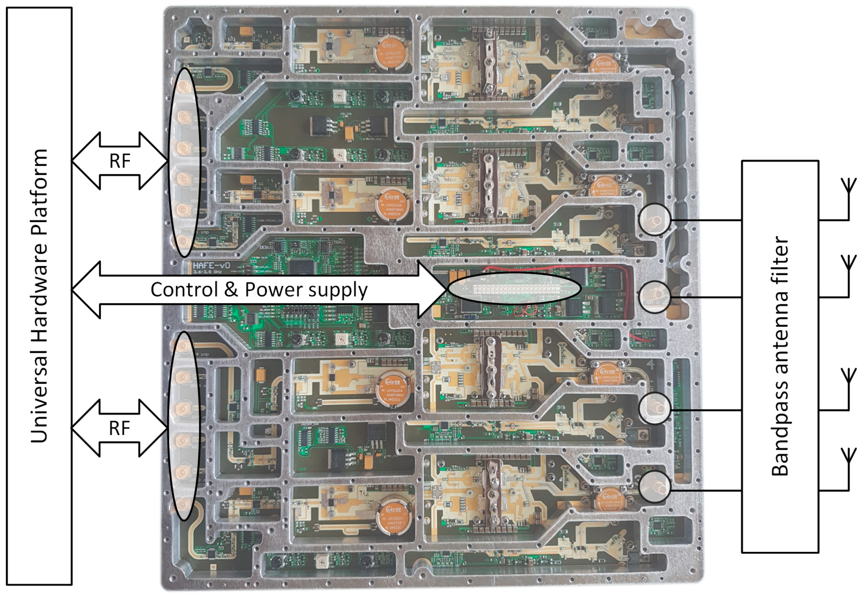
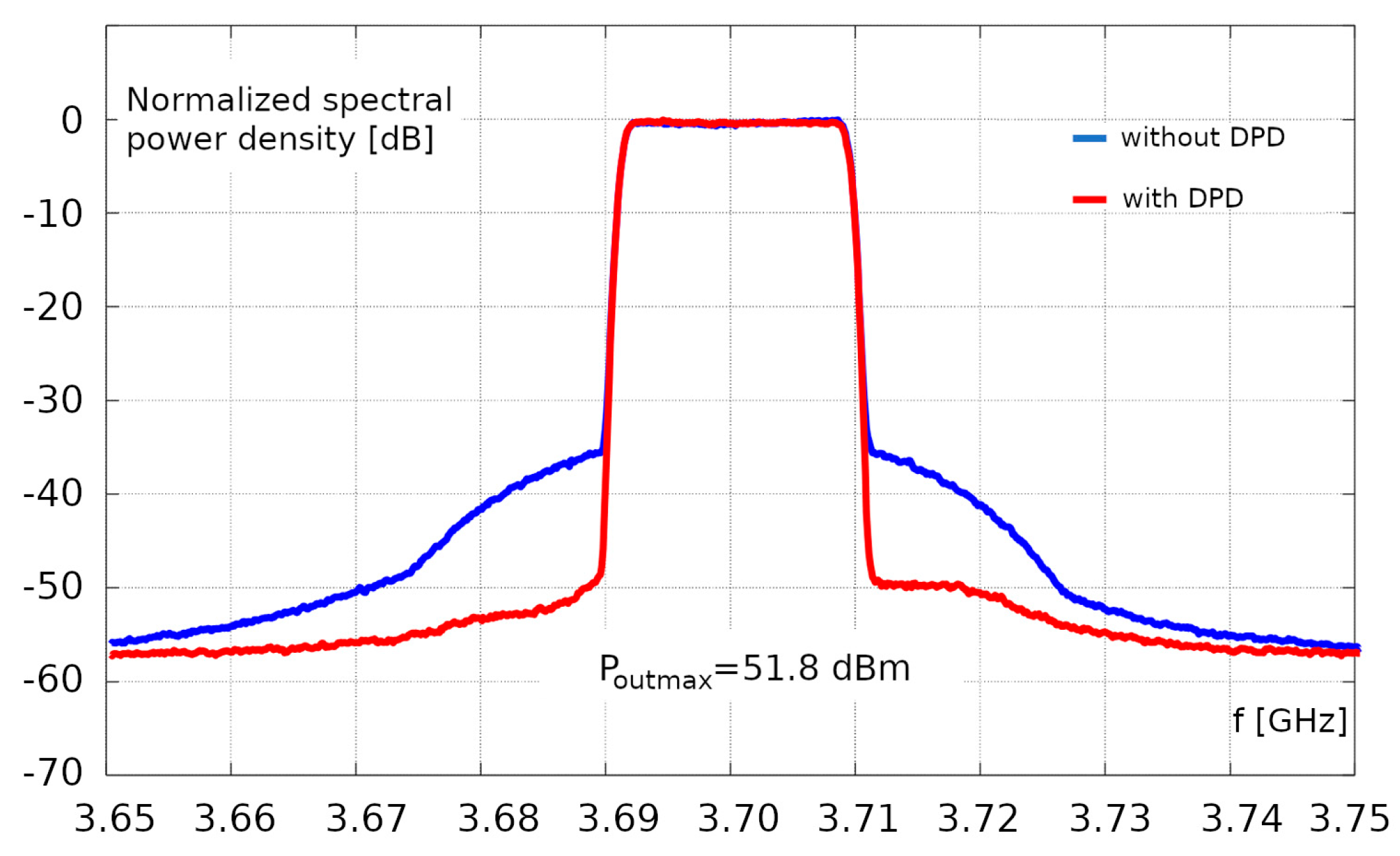
A view of the four-channel RF front-end board is depicted in
Figure 5. Exemplary characteristics of the TX path for the LTE 20 MHz signal with and without enabled DPD algorithm are shown in
Figure 6. RF TX and RX path parameters are briefly summarized in
Table 2.
5.2.2. B31 RF Front-End
The second developed RF front-end adapts the UHP to an LTE-A micro base station working with the frequency duplex FDD in the 452.5 MHz ÷ 457.5 MHz and 462.5 MHz ÷ 467.5 MHz bands for the receiver (uplink) and transmitter (downlink), respectively. A block diagram of one of four channels of the B31 RF front-end is shown in
Figure 7. Due to the similar structure and components used in both RF front-ends, the B31 RF channel is described briefly.
In an FDD system, the RF front-end must be fitted with a duplexer so that both the TX and RX paths work simultaneously. As shown in
Figure 7, a cavity duplex filter was used to separate downlink and uplink signals. The duplexer features a measured suppression higher than 80 dB of the transmitted signal in the receiver band. A limiter (LIM) with PIN diodes CLA4605-085LF (Skyworks Solutions) is located at the RX path input. As the LNA, the high linearity GaAs pHEMT IC amplifier SPF5043 (Qorvo) is operated. The SPF5043 noise figure is lower than 0.6 dB at a high 20 dB gain measured over a 450 MHz to 470 MHz frequency range. The digitally controlled attenuator HMC HMC624ALP4 (AD) adjusts the RX path gain to increase the receive signal dynamic. To constrain out-of-band nonlinear distortions produced by LNA and blocker signals from the antenna and four TX paths, a bandpass filter TB0267A (Golledge Electronics Ltd. (Illminster, United Kingdom)) was used. Repeating the SPF5043 and TB0267A components aims for the desired RX path gain.
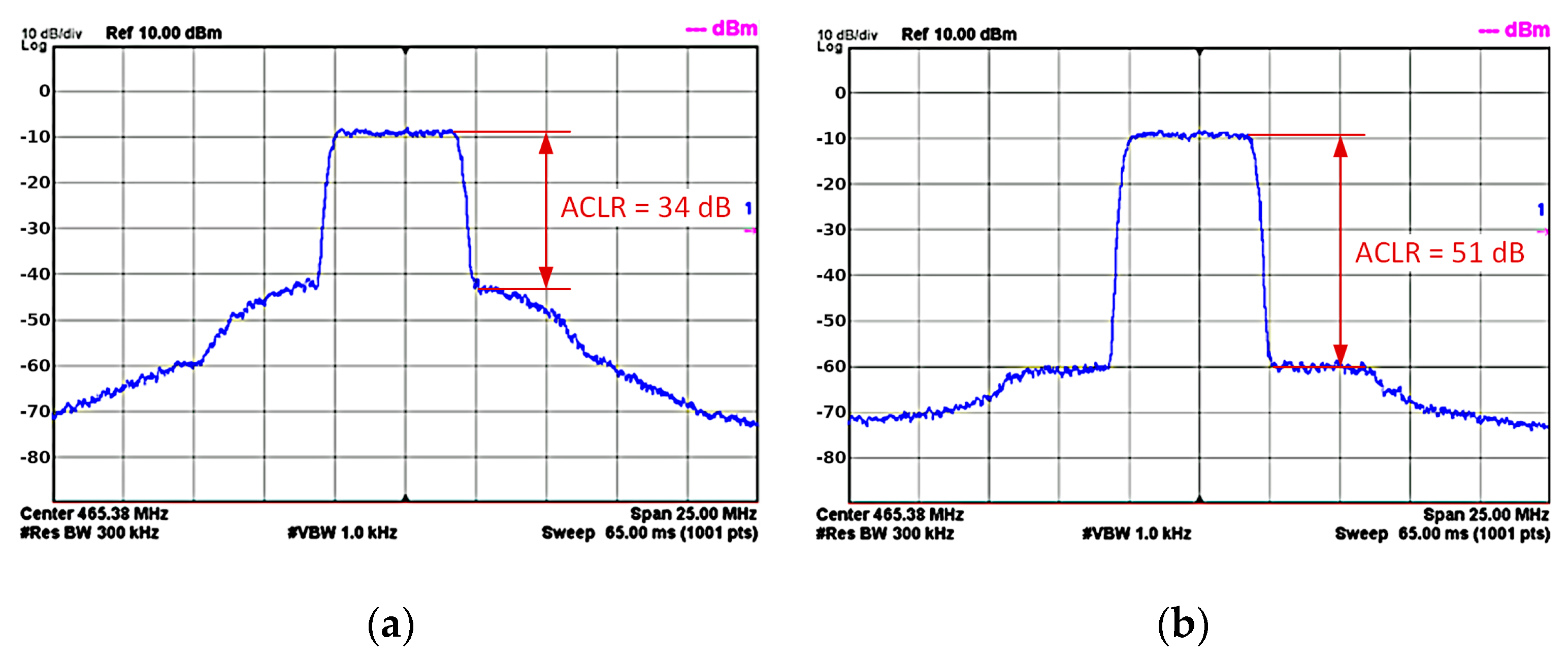
The TX path contains a chain of amplifiers with a final stage carried out in the Doherty configuration to maintain high efficiency over a wide amplitude change range of the input signal. The first two stages, SPF5043 and ADL5611 (ADI), work as preamplifiers. The digitally controlled HMC624ALP4 optimizes the signal level in the TX path. The Doherty amplifier was developed using two identical transistors, BLP10H610 from Ampleon. The BLP10H610 is a low-cost LDMOS power FET recommended for applications from HF to 1.4 GHz. It achieves 14 W output power with a gain of 25 dB in the 400 MHz ÷ 450 MHz frequency range under CW conditions. Due to proper phase shifts at the outputs of transistors, the DA could be designed in classical architecture. It is worth noting that Main and Peaking are operated in class AB and C, respectively. The DPA design was carried out using the ADS software with the implemented nonlinear BLP10H610 model delivered by Ampleon. The harmonic tuning method was employed to model the Main and Peaking stages and the complete DPA. Its measurements exhibited that the saturated output power was higher than 18 W at the 21 dB gain from 460 MHz to 470 MHz frequency range. The power-added efficiency (PAE) ranged from 73% to 77% in the wide output power range of 38 dBm to 42.5 dBm. The above results are obtained for the pulsed CW excitation with a 20% duty cycle. DPA efficiency for the LTE signals will be lower. The signal part from DPA is directed through a 35 dB coupler to AD9375 ORX input to execute the DPD algorithm dynamically. At the same time, the detector HMC1120 (ADI) monitors this output signal. A circulator placed at the TX path output isolates DPA and enables a reflected power from the antenna to be measured with another detector.
A photo of the four-channel RF front-end board is shown in
Figure 8. Example characteristics of the TX path for the LTE 20 MHz signal without DPD and with DPD algorithm implemented into AD9375 IC are shown in
Figure 9a,b, respectively. TX and RX path parameters of RF B31 front-end are listed in
Table 3. Measurements were performed with Keysight MXA N9020A spectrum analyzer.
5.3. Validation
5.3.1. Transmitted Signal Quality Assessment
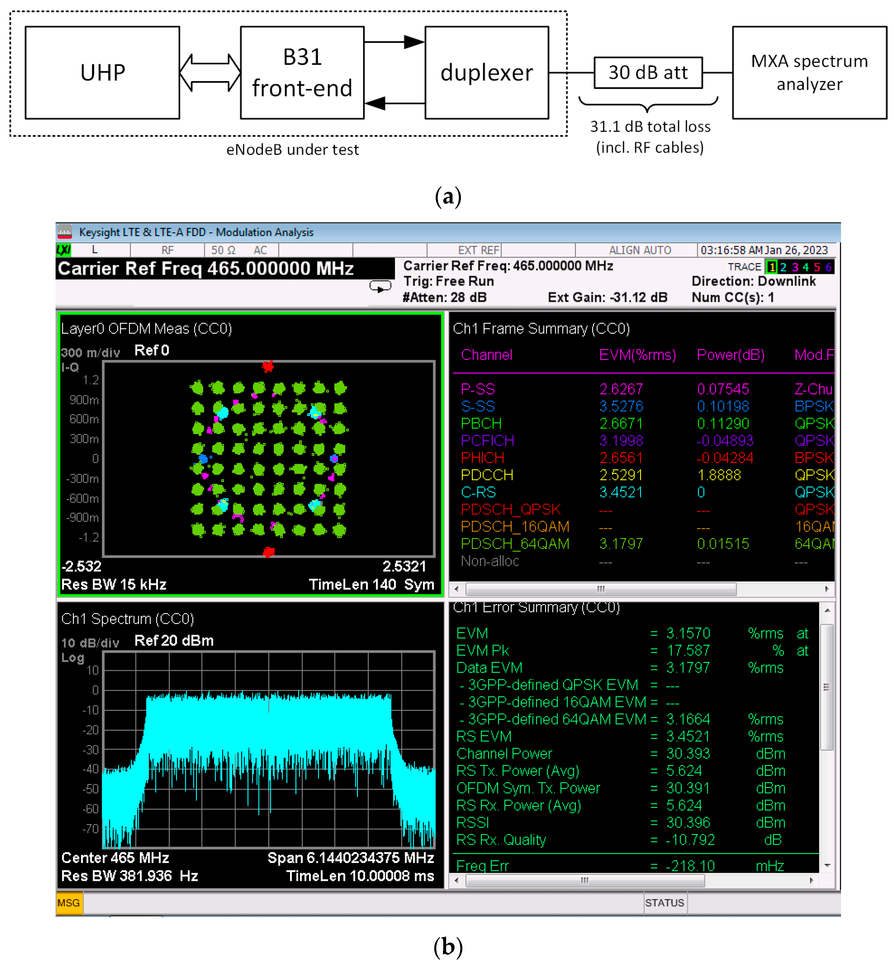
Before setting up the hardware for open field tests, several validations had to be performed. The central guides for hardware validation are requirements stated by ETSI [
50]. Due to the lower popularity of the B31 band, as an example, we present below the test results of the LTE micro base station working from 462.5 MHz to 467.5 MHz (downlink) and 452.5 MHz to 457.5 MHz (uplink) frequency range. As shown in
Figure 10a, the test fixture consists of eNodeB built with the UHP, B31 front-end and the duplex filter, and 31.1 dB lossy RF connection and Keysight MXA spectrum analyzer. The latter allows quality monitoring of transmitted RF signals. The following LTE configuration is used in the experiment: B31 RF band, 5 MHz nominal signal bandwidth, CFR enabled, enforced heavy traffic, and approx. 1000 mW of output power. The transmitted signal quality expressed by EVM values and the constellation diagram are presented in
Figure 10b (please make note that the diagram aggregates constellations for different physical channels, which are indicated with colors).
5.3.2. Performance Validation with Emulated User Terminals
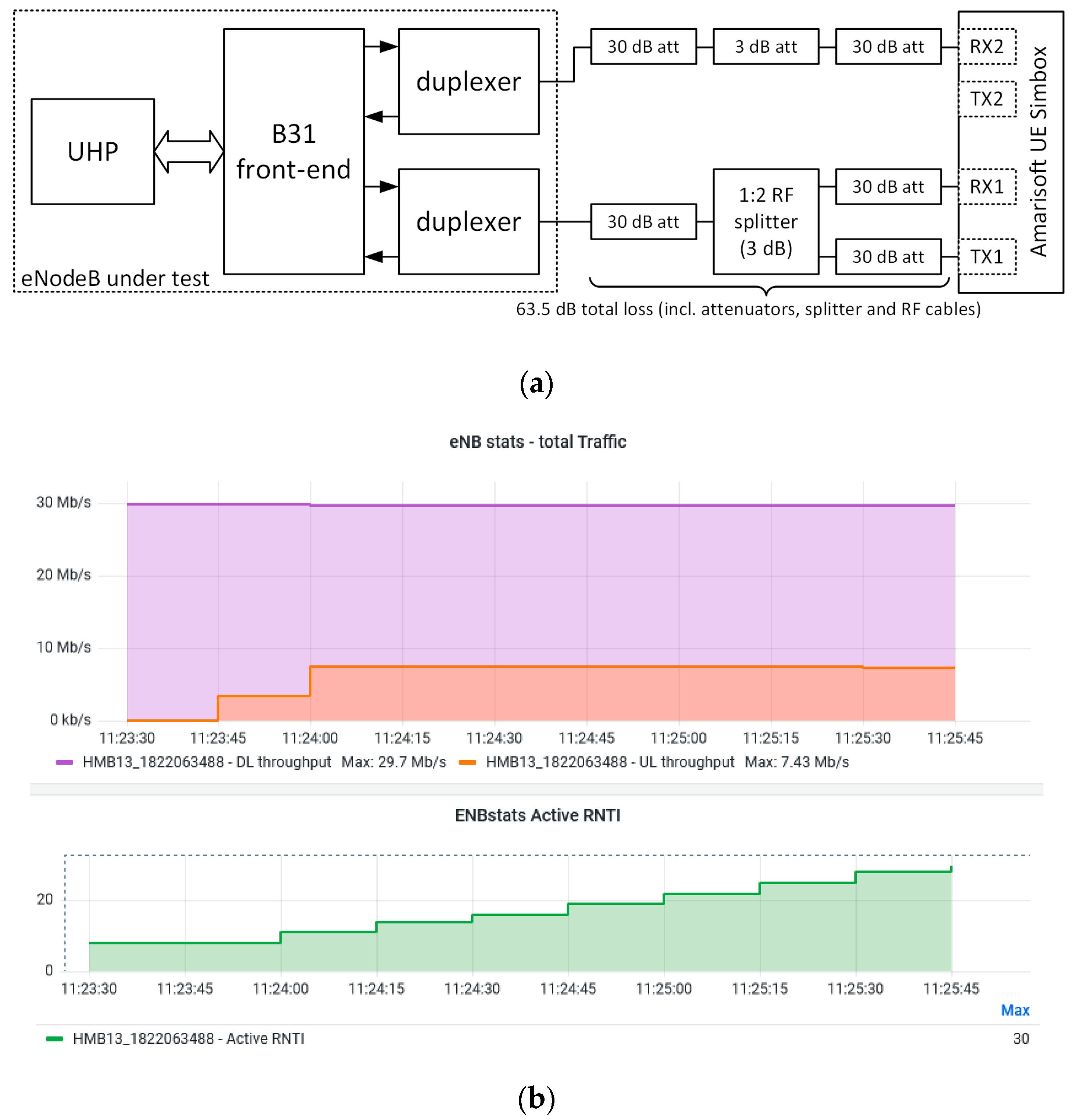
In another experiment, the overall performance of the eNodeB built on our Universal Hardware Platform has been evaluated. The text fixture is presented in
Figure 11a, and the LTE configuration is the same as presented in
Section 5.3.1. The Amarisoft AMARI LTE UE Simbox U is a popular device that emulates a certain number of user terminals within the coverage area of the eNodeB under test.
Figure 11b shows that our test fixture can achieve the throughput values (29.6 Mbps downlink traffic, 7.4 Mbps uplink traffic), which are close to the theoretical limits for 5 MHz RF bandwidth.
6. Conclusions
In this paper, we presented the Universal Hardware Platform based on the SDR technology for prototyping radio systems operating within the 300 MHz to 6 GHz range with simultaneous synthesis and analysis in the bandwidth of up to 100 MHz. The platform enables setting up a 4 × 4 MIMO. Adapting to the desired LTE band was achieved by attaching a suitable RF front-end and adjusting the software. RF front-ends still substantially affect the whole radio system performance; thus, special attention was paid to issues related to their implementations. Therefore, two examples of UHP cooperation with various RF front-ends were presented. In addition to different operating bands, LTE-A micro base stations prototyped using the UHP also work with other duplex schemes. Performance of both developed LTE-A setups is more than satisfactory. They are in line with expectations. Indeed, the use of UHP accelerated the prototyping of LTE-A micro base stations mentioned in the paper. We assess that the prototyping time became shorter by two-fold. The above facts prove the versatility and effectiveness of our platform in designing not only LTE micro base stations; it can also be employed in the R&D of hardware and software for the subsequent radio systems. In particular, UHP is a convenient tool for developing and testing DPD algorithms with various power amplifiers under representative conditions for a specific standard.
The platform described in the paper will be a subject of field trial in northern Poland. The goal of this campaign is to test the coverage and general system performance for the following applications: IoT, VoLTE, Mission Critical Push to Talk. Today, the UHPs are operated in LTE-A micro base stations to test links with subscriber terminals available on the market. Our plans include a new RF front-end for B255 band (5.8 GHz) as we observe a growing interest in this band among mobile service providers. Moreover, the expertise gained during UHP development and evaluation opens the way to R&D work on 5G/6G systems, which is the next step on our roadmap.


 ,
, 


