Abstract
This paper proposes a novel technique of TSV BIST repair that targets the design yield and various test challenges of three-dimensional integrated circuits (3D stacked ICs). The proposed methodology is efficient to cover the various faults during the fabrication, the interconnect breakages, shorts, bridges, void formation, thermal and physical stress, etc., during the TSV fabrication and stacking of 3D ICs. The repair mechanism provides a redundancy feature to replace the failing TSVs with spare TSVs in the design. It provides a significant impact on yield compared to the standard TSV testing approach. Further analysis was performed on different stacked levels of 3D ICs, and the results were compared with the existing industrial methods in terms of the yield and test time parameters. The proposed mechanism showed a significant improvement of 12.5% in the yield and 17.5% in the test time and also recovered all defective chips efficiently.
1. Introduction
In the context of high-performance computing, the integration of more computing capabilities with dedicated cores or accelerators to meet artificial intelligence (AI) demands poses more and more challenges. Due to the increased cost of advanced nodes and the difficulty of reducing analog input-output (IO) signals and circuits, replacing single-chip architecture solutions is becoming mainstream [1,2].
Three-dimensional (3D) IC technology is drawing attention as a leading solution for modern semiconductor industries. The 3D IC technology provides high density, high bandwidth, and less interconnect congestion to modern integrated circuits [3]. The through-silicon-via (TSV) integrate the multiple silicon dies on a single SoC (System on Chip), decrease the overall die area, and increase the performance and overall functionality of the design. Generally, the 3D stacked ICs are formed by combining different monolithic dies by keeping one die on top of another die instead of placing them side by side and connecting them; this process is called stacking or TSV bonding [4]. Though 3D IC technology provides multiple advantages over conventional 2D IC technology, it is only practically feasible when its production costs are commercially reasonable [3,5]. Similar to other components, the TSVs are also prone to defects, such as short, open, void formation and disconnects due to thermal stress, misalignment of pillars, random impurities, etc. All the 2D dies that are going to be stacked or bonded during 3D IC fabrication are considered good dies (KGD). In that case, if there is any fault in the TSVs during the bonding process, the complete 3D stacked die is considered a defective die, even though the individual 2D dies are defect-free. Due to the failing TSV, the complete 3D IC becomes faulty. It causes higher production costs and lower yields w.r.t. 3D stacked ICs [6,7,8,9].
Several strategies were studied in the past w.r.t. yield loss analysis, and a few research studies provided techniques to overcome these challenges, minimize the test cost, and improve the yield [10]. However, the authors took the common approach that the TSV faults are uniformly distributed and replaceable with adjacent TSVs [11]. Even though in practice, if one of the TSVs is active during the bonding process, the adjacent TSVs are probably more likely to be defective due to the clustering effects, which made the earlier TSV repair system less efficient and reliable [9,10,11].
In this paper, the introduction covers the requirements of 3D IC chiplet designs and the various challenges concerning 3D-stacked IC implementation. Section 2 covers the motivation of chiplet-based designs, various existing TSV BIST (built-in-self-test) techniques, and their challenges during the pre-bond and post-bond processes. The proposed TSV BIST methodology and new testing approach for the read group and write group TSVs are described in Section 3. In Section 4, the TSV BIST repair architecture and repair flow are explained with and without faulty TSV cases in the design. The detailed experimental results, yield analyses for different chiplet designs, and comparison tables are provided in Section 5. Section 6 discussed various challenges faced during TSV BIST implementation and future scope. Finally, the conclusion of the paper is mentioned in Section 7.
2. Motivation
The 3D IC fabrication process exhibited a relatively lower yield compared to the conventional 2D IC manufacturing process. Though 3D IC technology possesses an edge over 2D IC technology in terms of computation capabilities, it should also be commercially viable [10]. The unforeseen defects in via connections between the stacked multiple die of different nodes due to short, open, and void formation, etc. due to the uneven heights of TSV contributes to a notable loss of yield and performance of the overall chip [11]. Hence, an efficient design for testability methods should be developed to detect failures at an early stage of the process and minimize the yield loss and manufacturing cost as per the rule of ten [2,3,4,5]. This rule of ten is about the cost impact w.r.t. identifying the defect at various stages and the cost of resolving the defect at different stages of the IC design cycle.
The different stages of 3D IC testing mechanisms are shown in Figure 1. It gives a brief idea about how the monolithic dies are tested and stacked to form 3D stacked Ics. Currently, the following tests are being used for testing the 3D IC chiplets, 1) pre-bond TSV test (KGD: Known-Good-Die) [12,13,14] and 2) post-bond TSV test (KGS: known-good-stack) [15,16,17,18].
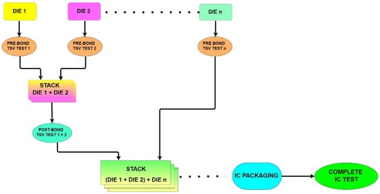
Figure 1.
Basic flow diagram for a 3D-stacked IC testing.
2.1. Pre-Bond TSV Test
A pre-bond test, also called a known good die, is mainly used to verify the TSV-related designs inside an individual die before they are entitled to the stacking process to make 3D chiplets. The KGD test has been proven to increase the yield of individual dies [9]. It targets the various clock and power network connectivity checks as well. The DFT (Design-for-Test) checks at individual dies are important since stacking a defective individual die unlikely into a multi-die chiplet may lead to the discard of the entire chip resulting in a huge impact on the yield and manufacturing cost [13]. Hence, the KGD test is also considered a screening test that inputs good quality dies into the multi-die IC stacking process [12,15].
However, the pre-bond test comes up with practical difficulties concerning the test accessibility due to limited test probe diameters and uneven distribution of small TSVs across the thin wafer. The built-in self-test techniques are said to be a solution for the above challenges, though they are not effective in detecting faults if the TSV logic is residing near the active device layer of interconnection [16]. Hence, discovering a potent testing methodology for TSV is mainstream.
2.2. Post-Bond TSV Test
A post-bond test, also called known-good-stack testing, is employed to make sure the TSV logic interconnections between the individual dies are proper and defect-free [17]. Even though the stacking has been performed with known good dies, there are still unavoidable conditions where failure might happen at the TSV bonding during the stacking process, which in turn results in discarding the complete multi-die chip that will contribute immensely to the yield loss and the total SoC manufacturing cost. As per recent studies, we have learned that the probability of TSV failures is directly proportional to the number of dies stacked in the chip [16,17,18].
Since all the wafers that are stacked into the chip come after the pre-bond TSV test. It will be easy to understand the failures caused after the stacking process. Though instead of discarding a multi-chip die after the tests, it would be highly profitable if a viable solution was identified to repair the failing bond between the dies, as the number of TSVs that fail at silicon used to be less, in numbers [19]. Figure 2 graph provides statistical analysis data of yield impact w.r.t variable faulty TSVs found during the post-bond TSV test for different layers of 3D-stacked ICs. This paper proposes a TSV BIST repair methodology that reports and as well as repairs the defective TSVs and supports the yield improvement and test cost of the 3D IC chip [20].
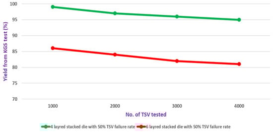
Figure 2.
Statistical analysis data of yield impact w.r.t. variable faulty TSVs.
3. Proposed TSV BIST Architecture and Test Methodology
The proposed TSVBIST architecture and the repair mechanisms are discussed in this section. Figure 3 depicts the architectural representation of the proposed TSVBIST repair mechanism. In a 3D-stacked IC architecture, there is a master die and many slave dies. The master die is usually the base chiplet, whereas the slave dies, or chips, are the dies that are stacked on top of the master die. The interactions between the master die and the stacked slave dies take place with the help of TSVs, and they also emphasize reduced interconnect congestion.
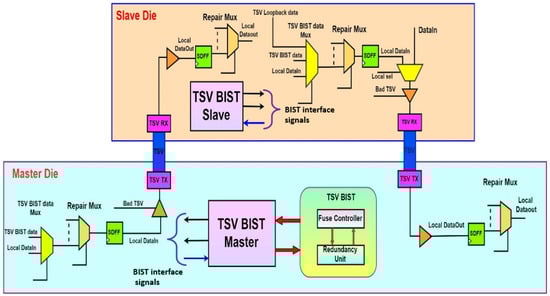
Figure 3.
Proposed TSV BIST repair architecture for 3D-stacked ICs (Reprinted with permission from ref. [21]. Copyright 2022 Springer Nature.
TSVs can be best described as a macro that has distinct transmitter and receiver components. The interactions between the stacked slave dies and master dies take place through these transmitter and receiver components. Since the stacking of multiple chiplets on a single die is inherently complex, the process of testing the TSVs is more demanding and cumbersome. Thus, more efficient and highly advanced test methodologies are required for ensuring the integrity of TSVs on stacked dies. This is vital for improving the yield and in the reduction of test costs. Therefore, to ascertain these factors and enhance the performance and productivity of TSVs, they should be grouped together and then tested. This reduces the test complexity and ensures the simplicity of the test mechanism.
When the TSVs are tested in a group, there is a significant decrease in test time. The physical location and count of the TSVs present within each block determine the size of the groups, and this size could vary from group to group. The most common grouping of TSVs occurs within the same block. The total number of TSVs present within a given block can be tested effectively by grouping them. Compared to this conventional testing by grouping on a block basis, the proposed methodology aims to group the TSVs based on their read/write operations. The TSVs based on the read groups are tested together, and similarly, the TSVs based on the write group are tested together. Each group can accommodate nearly 70 to 80 TSVs per group. The proposed architecture also incorporates two redundant TSVs within each group. These redundant TSVs are added as a failsafe mechanism to repair the defective TSVs identified during the testing by the TSV BIST repair mechanism.
The highlight of the proposed architecture is the built-in self-test mechanism (BIST). This mechanism enables self-testing across all TSVs. They also have the capability for the analysis of repair and redundancy in failing TSVs. It can be noted that the presence of TSV BIST logic is observed in each die. Those that are present as part of the master die are called the TSV BIST master and those that are seen in the stacked slave chiplets are called the slave TSV BIST. The functionality of the TSV BIST master is to trigger TSV BIST for different functional modes. It also governs the operation of the slave TSV BISTs in the stacked slave dies. The JTAG (Join Test Action Group) test data registers (TDRs) are programed to provide the required information concerning the execution, to the master die. Another important function of the TSV BIST master is fuse controller interfacing. This interfacing helps to drive the information related to repair and force the dispensation of fuses. Multiple components are associated with the TSV BIST master. These include data generators for BIST, address generators, and BIST comparators for comparison. On the contrary, the slave only has the data generation unit. They do not have an in-house data comparator. Conclusively, the data comparison is isolated to the TSV BIST master, in the master die. A single control signal enables the synchronization between the BIST master and BIST slave logics, in the master and slave die, respectively. This also ensures that multiple control signals are used for interfacing between the master and slave. This control signal is called the TSVBIST_CONTROL. As shown in Figure 3, the arrows of the “TSV BIST Master” and “TSV BIST Slave” represent the BIST test interface and control signals. It will provide the required test data inputs to the TSV macros and capture the corresponding test responses from the data comparator logic. It also controls the inputs and select lines of the repair MUX and TSV BIST data MUX in the design.
The TSVs are tested at rated highspeed frequency. Thus, multiple TSV BIST masters are required for each clock domain when multiple clock domains are involved.
From the architecture shown in Figure 3, it can be observed that for each TSV macro, two multiplexers are present at the transmitter, whereas only a single MUX is present at the receiver end. On the transmitter side, one MUX is the TSV data MUX and the other is the TSV repair MUX. The TSV repair MUX is also present in the receiver end, and this helps in shifting out the TSV data from one TSV to the next upon identification of a failing TSV macro. To ensure that the timings are met as per requirement, a pair of flip-flops and buffers are added. This also ensures that the shifting and capture operations are happening as expected. During EXTEST mode, these flops act as wrappers and are hence called wrapper flops. They act as normal scan flops to generate patterns and are connected to the scan chain during the SCAN mode of operation. Once a failing TSV is identified, it is swapped with the redundant TSV. The swapping occurs by shifting all the signals from the failing TSV to the spare or redundant TSV. If no such failure is identified, then all the signals are identified as passing through the existing TSVs.
The proposed methodology revolves around the concept of grouping TSVs into two groups, namely TSV read groups and TSV write groups. In the former, the data path is from the stacked slave die to the master die, whereas in the latter, the data path is from the base die to the subsequently stacked dies. The TSV BIST controller can provide the group number, which in turn decides whether a given group is a read or write group. The controller also oversees the execution of a given TSV group and records the pass-fail status. The testing occurs singly per TSV group and ensures that the entire group is covered thoroughly. To identify all the possible faults associated with TSVs within a given group, different patterns are applied. The idea behind TSV read-and-write group testing is highlighted in the subsequent sections.
As seen in Figure 3, the redundancy unit and the fuse controller interface present inside the TSV BIST architecture provide a repair mechanism similar to that of the MBIST (Memory Built In Self Test). The functionality of the redundant unit is the identification of the failing TSVs by observing the status register. It also estimates the repair signatures for each failing TSV. These repair signatures are stored inside a read-only memory (ROM) called the fuse controller. The fuse controller consists of a memory device, usually a read-only memory (ROM), that stores the repair signature values for all the repairable TSVs in the design.
The main difference between the standard TSV BIST test and the proposed TSV BIST approach is, the standard TSV test considers TSV to be an interconnecting wire and is tested by using the built-in-self-test approach. Additionally, there is no repair feature for faulty TSVs, and it leads to droppage in production yields. Here, the BIST logic needs to generate the test patterns for each TSV present in the design, so it creates the extra area overhead for individual address and data generator logics present in the BIST FSM (Finite State Machine) module. Additionally, there is no parallel testing mechanism in the standard TSV BIST approach; it increases the overall TSV testing time in the 3D-stacked IC design. Whereas in the case of the proposed TSV BIST test approach, created a separate TSV grouping mechanism called read group and write group TSV testing based on the die-to-die communication directions. It creates a great impact on the overall test time of the TSVs. Since all the TSVs present in read and write groups were tested simultaneously. Additionally, the proposed TSV BIST mechanism provides the repair feature to replace the failing TSVs with redundant TSVs in the design. It gives a significant yield improvement to the overall design. All the TSVs in a group are tested simultaneously due to this parallel testing mechanism, the BIST FSM logic area overhead will reduce, and we can reuse the same patterns for multiple TSVs in the design. Compared to the conventional TSV BIST logic, the proposed TSV BIST logic uses less area overhead as well.
3.1. TSV Read Group Test
The data transfer between the stacked dies and the master die occurs via the TSV read groups. The data generator is shared between the TSV master and the TSV slave. The TSV master must know at what point the valid data driven from the TSV slave needs to be compared since it has the in-house data comparator. The synchronization between the master and the slave is taken care of by the TSVBIST_CONTROL signal. Additionally, the comparator knows at what point it needs to compare the data based on the known number of flops between the slave and master. The data path between TSV BIST master and slave is depicted in Figure 4.
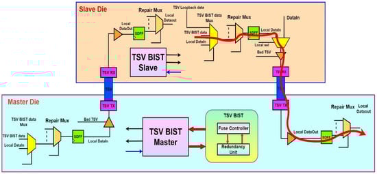
Figure 4.
Read Group data path in TSV BIST Repair flow for 3D ICs.
The TSV BIST data MUX is present in the stacked slave die, and these take the TSV BIST data as the input. The data is transmitted through one of the flops in the slave die and another flipflop situated in the master die. This transmission takes place before the comparator in the master die can compare the actual transmitted data with the expected data. Therefore, in the read data group, the data path comprises two flip-flops, namely the one in the stacked die and the other in the slave or base die. Additionally, in such a scenario, the maximum number of test pattern combinations that can be tried is four. In conclusion, four different combinations of test patterns are applied, and the response is compared using the in-house comparator in the master die. To identify all possible vulnerabilities in the TSVs, multiple applications of these four test patterns up to the width of the read group are required. At times, for the shift register whose width is equal to the width of the TSV read groups, applications of inversion to the base data pattern can occur depending on the contents of the shift register, and, in such cases, for the selection between the actual data and the inverted data, the TSV data select register is utilized.
The identification of the failing TSV in the read groups happens through the BIST status registers. Upon encountering such failures, the execution of the algorithm pauses, and the redundancy analysis unit begins the estimation of the repair signature. Once the repair signature is ready, the fuse controller within the TSV BIST master stores these values. Once the failing information is stored, the TSV BIST matter dispenses all the repair signatures. These swap the failing TSVs with the redundant TSVs. Once the repair sequence is completed, the TSV master is notified and the algorithm for testing resumes. As discussed, the TSV BIST status register determines whether a repair is needed or not. This register is two bits, wide per group.
In Figure 5, up to four dies are stacked one on top of the other. The read group operation is depicted here. Consider two different scenarios, where, two slave dies are stacked on top of one master die, and three slave dies are stacked on top of a master die. The data path is from slave die to master die in the case of a read operation, as shown in Figure 5.
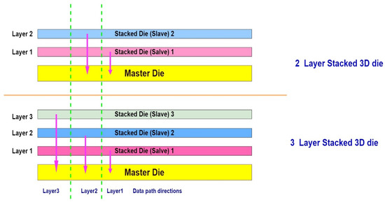
Figure 5.
Read group data paths in TSV with respect to multi-layer 3D SICs.
Since we are incorporating two redundant TSVs per group, a maximum of only two repairs can be performed in case of failure. If more than two failing TSVs are present in any given group, then those TSVs are flagged as irreparable, and a fatal error is thrown. The repair register contains the details of both the read groups as well as the write groups. The lower-order bits belong to the former, whereas the upper-order bits belong to the latter. The details about the 2-bit BIST status register are shown in Table 1.

Table 1.
Repair status register values of TSV BIST.
3.2. TSV Write Group Test
The TSV write group test is basically to test the write group, even though to perform a write group test, we must test the read groups upfront as the write groups are tested by looping back the read group. Once the TSV read group test is completed, as illustrated in Section 3.1, the next procedure is the TSV write group test. In a glimpse of the complete procedure, the data sent from the master die to the slave die is again looped back in a similar manner from the slave die to the master die. The master die contains the TSV BIST data MUX, which configures to select the TSV BIST data from the master die and propagates the data to slave dies and stacked dies feedback the received/written data through a total of 4 flops to the TSV BIST comparator present in the master die for data evaluation along with the read groups. The flops in the data path are significant since the data loops over four different data patterns, and the comparator will be aligned with the correct data once it has propagated through the feedback path back to the master die.
Since the write group testing is performed in aid of the read group, the same vectors can be used for the read group test as well. In case the number of total write groups is higher than the number of total read groups, then the read groups might be repeatedly used for the write group testing. The data path for write group testing, which consists of the data propagation from the master die to the slave die and then loopback from the slave die to the master die is shown in Figure 6.
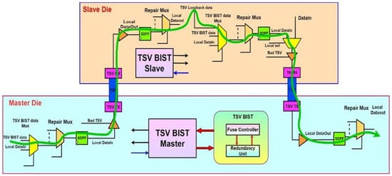
Figure 6.
Write Group data path in TSV BIST Repair flow for 3D ICs (Reprinted with permission from ref. [21]. Copyright 2022 Springer Nature.
As we see in Section 3.1, after applying all the data vectors to the write group, the failed TSVs are identified with the help of BIST status registers. Once any TSV failures are reported by the status registers, immediately the process must be paused, and the repair signature is generated by the redundancy analysis unit and exported into the fuse controller present in the TSV BIST master. The fuse controller unit receives all the repair signatures and will send them to all failing TSVs through the TSV BIST master to process the repair mechanism.
The basic write operation performed by the various layers of stacked slave dies is illustrated in Figure 7. As we have seen in Section 3.1, even here we are considering the 2 various configurations of different layers of the stacked slave dies, such as 2 layer, and 3 layer of stacked 3D dies. In all the scenarios, the write operations are performed from a master die to a slave die and read operations are performed from a slave die, to a master die.
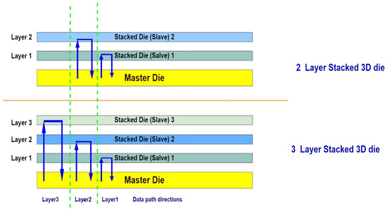
Figure 7.
Write Group data paths in TSV with respect to multi-layer 3D SIC’s.
Figure 7 illustrates the complete write group test, data transversal path, from the master die to the slave die and feedthrough from the slave die to the master die. The fuse controller inside the TSV BIST master consists of 32-bit fuse registers, as shown in Figure 8. It stores all the repair signature values generated by the redundancy analysis unit. The repair signatures consist of all the repair information. The different bits inside the fuse register point to a failing TSV. It consists of the 10-bit slave die ID and similar to the 10-bit TSV group ID and the 12-bit repair signature values.

Figure 8.
Fuse Register for TSV BIST Repair ICs (Reprinted with permission from ref. [21]. Copyright 2022 Springer Nature.
4. TSV BIST Repair Architecture and Implementation flow
Till now we have seen how the TSVs are grouped and tested together, this section provides detailed information about the TSV BIST repair mechanism and repair distribution flow. Similar to the conventional memory BIST approach, the proposed TSV BIST repair architecture also consists of a redundancy mechanism with the help of a fuse controller and redundancy analysis unit interfaces, as shown in Figure 9. Here, the redundancy analysis unit provides the facility to identify the failing TSVs based on TSV BIST status registers, and it will calculate the repair signature values for the failing TSVs in the design. The fuse controller is a kind of non-volatile memory (ROM), and it will store the repair signature values of all the TSVs present in the design. TSV BIST enables the repair distribution mechanism to provide the repair signature to every TSVs present in the design.
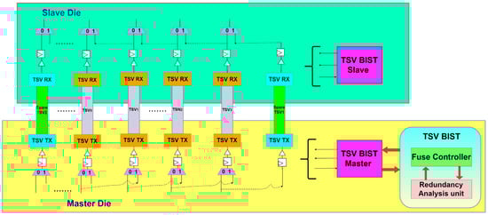
Figure 9.
TSV BIST Repair Architecture.
As mentioned earlier each TSV group consists of 2 spare TSVs to perform the repair operation. With this, we can be able to repair up to 2 failing TSVs in the design. The optimal number of redundant TSVs in a group is decided by the various experiments conducted and analyzed the results w.r.t different performance indicators, such as yield and area etc. For simple understanding, purposes considered the two spare TSVs which is in green color sitting left and right side of the normal TSVs shown in Figure 9.
Each TSV consists of a pair MUXs at Transmitter and Receiver sides, these MUXs are used for repair purposes. The MUX select line is controlled by the TSV BIST logic which is presented in both master and slave dies. Based on the failing TSV location MUXs select line will change to bypass the failing TSVs in the design. During the TSV BIST test, if there are no failing TSVs present in the design, in that case, the data communication is directly routed through the dedicated TSVs which are already connected from the master die to the slave die in the design. You can see the data path which is in blue color arrow lines driving from the master die to the slave die shown in Figure 10.
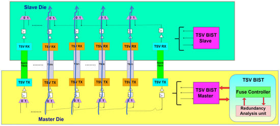
Figure 10.
TSV BIST Repair flow in case of no fault in the TSV group.
Let us consider if any one of the TSVs is failing (assume TSV2 in Figure 11) in the group and identified during the TSV BIST test. In this scenario, the TSV BIST Redundancy analysis unit identifies the failing TSV location and calculates the repair signature, and stores it in the fuse controller. Whenever the failing TSV is identified the repair mechanism distributes the repair signature to replace the failing TSV with a spare TSV in the design. Figure 11 observes that for the first two TSVs TSV0 and TSV1 drive the data as it is without changing any data path. When it comes to the failing TSV2 data path it routes through the next TSV (TSV3) data path and the TSV3 data path shifted to TSV4 and so on. Finally, the last TSV[N-1] data path route through the spare TSV data path is shown in pink colour arrow lines in Figure 11. Here the data right shift happened through the repair MUXs sitting on either side of the TSVs and the MUX select lines are programmed through the TSV BIST controller.
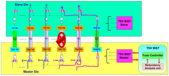
Figure 11.
TSV BIST Repair flow in case fault in TSV group.
A TX repair MUX shifts logical bits to a wider bus, and an RX repair MUX constructs the original logical bus on receiving side, it avoids the broken TSV(s) when transmitting/receiving data across dies. By default, data is transmitted on TSVs 0 through N-1. TSV BIST sends group repair information to FUSE controller during BIST for distribution to all dies and repairs the group during the BIST test. The TSV BIST FSM ‘waits’ for a ‘resume’ from FUSE controller and a second PASS TSV BIST on the same group ensures the repair worked. Here, the TSVs are used for fuse distribution, clock, and control signal purposes and do not come under any of the TSV groups and those are non-repairable TSVs.
The actual transmitter and receiver repair MUXs implementation with 3 shifts vectors flow is described below:
Let’s assume N = width of the group, the number of spare TSVs per group is fixed at 2, and the repair MUX computations are as below:
ShiftDecode0[N+1:0] = {(N+2) {RepairValid0}} << Repair0
ShiftDecode0[N+1:0] = {(N+2) {RepairValid0}} << Repair0
RawShift2[N+1:0] = ShiftDecode0[N+1:0] & ShiftDecode1[N+1:0]
TsvShift2[N+1:0] = {RawShift[N+1], RawShit2[N+1:1]}
TsvShift0[N+1:0] = ~ShiftDecode0[N+1:0] & ~ShiftDecode1[N+1:0]
TsvShift1[N+1:0] = ~TsvShift0[N+1:0] & ~TsvShift2[N+1:0]
Compute Final Repair Shifted DataOut[N−1:0] That Extracts Repaired Data from the TSV Group:
DataOutPre[N+1:0] = (TsvShift0[N+1:0] & {TsvIn[N+1:0]}) |
(TsvShift1[N+1:0] & {1′b0, TsvIn[N+1:1]}) |
(TsvShift2[N+1:0] & {2′b0, TsvIn[N+1:2]});
DataOut[N−1:0] = DataOutPre[N−1:0]
DataOutPre [N+1:N] − Unused.
The below diagram gives a detailed idea about the repair MUX structure and its functionality, let us consider 2 TSV groups named Group-A and Group-B. the TSV to data shift paths and repair MUX select line operations for Group-A and B as shown below in Figure 12.
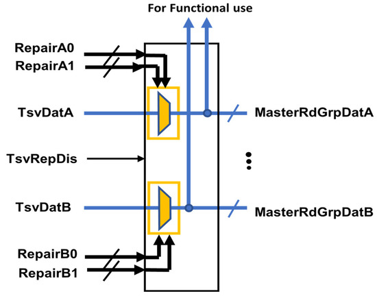
Figure 12.
Repair MUX structure.
TSV BIST Repair Flow
In this proposed TSV BIST repair flow, we ran the TSV BIST test three times (passes) on the same TSV group.
Pass 1: This is the first run.
If no errors are found, the group test is performed (move to the next TSV group).
If one or two errors are found, repair signatures are generated and sent to the fuse box or fuse controller reloading is requested so the fuse controller can fetch the generated repairs from the fuse box and send them to the tested TSV group for repair purpose
Pass 2: The same test is repeated on the same TSV group
If no additional errors are found, the group test is performed (move to the next TSV group).
If one additional error is found (with a total of <3 errors in Pass 1 ana Pass 2), a new repair signature is generated and sent to the fuse box. Then repair reloading is requested, such as in Pass 1.
Pass 3: The same test is repeated on the same TSV group for the third time. If any error is found. Fatal Error is set.
If additional errors are found (a total of 3+ errors in Pass 1 and Pass 2), the TSVs group test is performed. Fatal Error is set.
If 3+ errors are found in Pass 1, Fatal Error is set.
5. Results and Yield Analysis
The proposed TSV BIST repair architecture mechanism was implemented in various industrial designs and the performance of the proposed methodology was analyzed on various 3D chiplet designs with different layers. The extensive yield analysis was performed on various types of chiplet-based designs and compared those yield results with standard TSV BIST approaches. The manufacturing defects in TSVs causes during the pre-bond and post-bond process of TSVs, it causes huge yield losses in the design. To repair such kind of failing TSVs, our proposed approach significantly overcomes the faulty TSVs and yield gaps. The conventional TSV BIST techniques follow the simple interconnect testing mechanism, and it tests individual TSVs in the design. The proposed TSV BIST repair approach provides a novel TSV grouping mechanism to improve the yield and reduces the overall TSV testing time in the designs. In this section, we discuss the detailed analysis of yield, test time, and area overhead concerns w.r.t. various 3D chiplet-based design results. Here, the monolithic dies that are going to be stacked are fault free and tested during the TSV pre- and post-bond testing phases.
The results are analyzed on two different types of 3D chiplet designs (3 layers 3D ICs, and 6 layers 3D ICs). Additionally, the same results compared with the standard TSV BIST approach. The proposed TSV BIST repair mechanism is implemented on heterogeneous 3D chiplet designs, whereas the standard TSV BIST approach is performed on homogenous chiplet-based designs. The complexity and test times are high in the case of heterogeneous designs when compared with homogeneous designs. Approximately 75–80 TSVs are used in read-and-write group TSVs.
For each 3D chiplet design (3 layers and 6 layers) results were analyzed on two different sets of manufactured ICs, the first set consisting of 100 K chiplets and the second set consisting of 200 K chiplets. During the testing of 100 K chiplets the proposed TSV BIST repair methodology, gives 92% and 96% yields w.r.t 6 layers and 3layers 3D designs. Whereas the standard TSV testing approach gives 81% and 84%, respectively. Similarly, during the testing of the second set of 200 K chiplet ICs, the proposed TSV BIST Repair methodology gave 85% and 88% of yields w.r.t 6 layers and 3 layers designs. Whereas the conventional TSV testing approach gives 72% and 77%, respectively. There is a difference in yield % w.r.t different layers of 3D stacked dies. This is due to the chances of faulty TSVs present in 6 layers stacked dies being more compared to 3 layers stacked dies. Since the 6-layer stacked dies have more numbers TSV interconnects and the chances of existing faulty TSV in the design is more when compared to 3 layers stacked dies. The overall yield analysis is shown in Figure 13, and the summary of the yield results is provided in Table 2. This extensive yield analysis has proven that the proposed TSV BIST repair mechanism provides a great improvement in the overall design yield of approximately 12.5%.
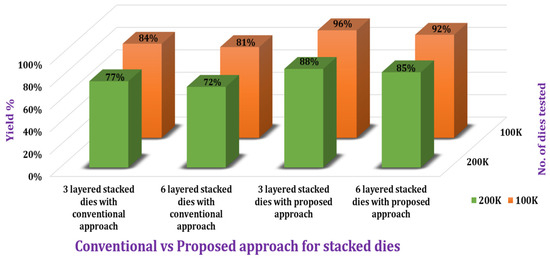
Figure 13.
Yield analysis graph between conventional and proposed TSV BIST approach (Reprinted with permission from ref. [21]. Copyright 2022 Springer Nature.
Table 2.
Yield numbers in standard and proposed TSV BIST Repair approach.
In this proposed approach, the TSVs are grouped and tested together, which reduces the overall test time of the TSVs as well. The average testing of each die was analyzed w.r.t 6 layers and 3 layers and compared the testing time w.r.t conventional TSV testing approach. The average testing of 6 layers and 3-layers 3D chiplet is 1.23 s and whereas the conventional TSV testing approach takes an average of 1.52 s to test the 3D chiplet IC. The test time analysis is shown in Figure 14. Therefore, the average gain in overall TSV test time is ~17.5%.
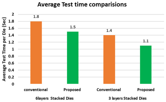
Figure 14.
TSV test time Analysis graph between Conventional and Proposed TSV BIST approach.
The yield of the chiplet designs was analyzed at various levels of open defect ratios. It performs the proposed TSV BIST repair approach. It also provides the lower and upper limits of the number of possible defects for achieving the maximum yield with a minimum area overhead. The 3D chiplet yield behavior with different levels of open defect ratios is provided in Figure 15.
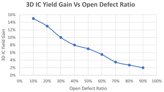
Figure 15.
Three-dimensional IC yield gain vs. open defect ratio.
The proposed TSV BIST repair architecture creates a minimal area overhead since all the TSVs in a read group or write group are tested simultaneously. Due to this parallel testing mechanism, the overall BIST FSM logic size reduces, since we can reuse the same patterns for multiple TSV groups in the design. Whereas in the case of the traditional TSV BIST approach, the TSVs are treated as interconnect wires and the BIST FSM needs to generate the individual patterns for each TSVs present in the design. Here, the size of the BIST FSM w.r.t address and data generator logic increases, and it causes the extra area overhead to the design. At the same time, the proposed method needs extra fuse registers to store the repair signatures for failing TSVs. From the overall fuse controller, we are allocated 1024 fuse registers to 3D-stacked IC and 1408 fuse registers to 6 layers, 3D-stacked IC to store the repair signature for faulty TSVs in the design. Whereas in the case of the traditional TSV test approach, separate fuse, registers are not required since there is no repair feature for the traditional approach. Compared to the conventional TSV interconnect testing, the proposed TSV BIST repair mechanism consumes less area overhead and is negligible compared to the benefits provided by the whole design. The below Table 3 and Figure 16 describes detailed information about the extra gate count and fuse length required to implement the TSV BIST logic and the percentage of area overheads of TSV BIST logic during the conventional approach as well as in the proposed approach.
Table 3.
Area Overhead comparison.
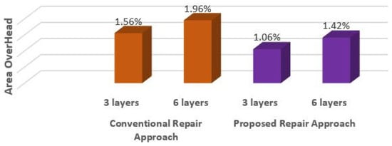
Figure 16.
Comparison between proposed Vs Conventional TSV BIST area overheads.
6. Challenges and Future Scope
This section captures the various challenges faced during the implementation of the proposed TSV BIST repair mechanism. The TSV BIST master and slave logic used for testing the TSVs consumes extra space overhead. Performing the TSV BIST repair operation needs extra fuse allocations and bootup sequences, which creates a huge area overhead problem. The pre-silicon validation of the TSV BIST repair mechanism is a bit complex compared to traditional memory BIST validation. Since it requires creating the test benches for each individual die that is going to be stacked, it takes a long time to validate the stacked dies. The testbench setup creation is complex, and for validation, TSV BIST repair needs to keep all the staked dies in a single testbench. To test the slave, dies always need to provide the test sequence from the base die or master die, which requires an extra bootup sequence during the silicon bring-up phase when the chip is powered on. It increases the overall bootup sequence time. Nowadays, all industries and researchers are working towards overcoming the above-mentioned challenges with respect to advanced node technology designs. This proposed TSV BIST repair mechanism cannot be used during the wafer sort test or individual die (2D die) test. It is used only to test the 3D-stacked ICs during the staking or TSV bonding phase, also called the packaging test.
7. Conclusions
In the above sections of this paper, we have discussed a novel methodology for TSV BIST repair that is capable of covering the various defects, such as open, shorts, and interconnect breakages, during the stacking and fabrication process of three-dimensional ICs (3D stacked ICs) as the solution to the struggling yield and test complexities. The proposed methodology also provides the diagnosis and repair capabilities for failing TSVs in 3D chiplet designs to achieve the targeting goals w.r.t. test time and yield. A novel TSV grouping mechanism is also introduced in this paper based on TSV read and write operations. The test was conducted and performed on various sets of 3D stacked devices with respect to 3-layer and 6-layer designs, and the results were compared with the traditional TSV test approaches in terms of yield and test time. We have seen a 12.5% yield improvement with respect to the proposed methodology. Additionally, we have seen a drastic savings of 17.5% in the testing time compared to the conventional methods. Additionally, compared to the conventional TSV testing, we have identified and proven that area overhead is minimal in the proposed methodology for the TSV BIST repair approach.
Author Contributions
Methodology, R.S.V.E.A.; Validation, R.S.V.E.A.; Investigation, R.S.V.E.A.; Writing—Original draft, R.S.V.E.A.; Writing—Review & editing, S.S.; Supervision, S.S. All authors have read and agreed to the published version of the manuscript.
Funding
This research received no external funding.
Data Availability Statement
Not applicable.
Conflicts of Interest
The authors declare no conflict of interest.
References
- Xu, K.; Yu, Y.; Peng, X. TSV Fault Modeling and A BIST Solution for TSV Pre-bond Test. In Proceedings of the 2021 IEEE 39th VLSI Test Symposium (VTS), San Diego, CA, USA, 25–28 April 2021; pp. 1–6. [Google Scholar] [CrossRef]
- Cheng, S.-F.; Huang, P.-T.; Wang, L.-C.; Chang, M.-C.F. Built-In Self-Test/Repair Methodology for Multiband RF-Interconnected TSV 3D Integration. IEEE Des. Test 2019, 36, 63–71. [Google Scholar] [CrossRef]
- Jani, I.; Lattard, D.; Vivet, P.; Durupt, J.; Thuries, S.; Beigné, E. Test Solutions for High Density 3D-IC Interconnects—Focus on SRAM-on-Logic Partitioning. In Proceedings of the 2019 IEEE European Test Symposium (ETS), Baden-Baden, Germany, 27–31 May 2019; pp. 1–2. [Google Scholar] [CrossRef]
- Wang, R.; Deutsch, S.; Agrawal, M.; Chakrabarty, K. The hype, myths, and realities of testing 3D integrated circuits. In Proceedings of the 2016 IEEE/ACM International Conference on Computer-Aided Design (ICCAD), Austin, TX, USA, 7–10 November 2016; pp. 1–8. [Google Scholar] [CrossRef]
- Jani, I.; Lattard, D.; Vivet, P.; Beigné, E. Innovative structures to test bonding alignment and characterize high density interconnects in 3D-IC. In Proceedings of the 2017 15th IEEE International New Circuits and Systems Conference (NEWCAS), Strasbourg, France, 25–28 June 2017; pp. 153–156. [Google Scholar] [CrossRef]
- Kumar, A.; Reddy, S.M.; Becker, B.; Pomeranz, I. Performance aware partitioning for 3D-SOCs. In Proceedings of the 2012 International SoC Design Conference (ISOCC), Jeju Island, Republic of Korea, 4–7 November 2012; pp. 163–166. [Google Scholar]
- Chi, C.; Lin, B.-Y.; Wu, C.-W.; Wang, M.-J.; Lin, H.-C.; Peng, C.-N. On Improving Interconnect Defect Diagnosis Resolution and Yield for Interposer-Based 3-D ICs. IEEE Des. Test 2014, 31, 16–26. [Google Scholar]
- Salah, K. DfT techniques and architectures for TSV-based 3D-ICs: A comparative study. In Proceedings of the 2016 18th Mediterranean Electrotechnical Conference (MELECON), Limassol, Cyprus, 18–20 April 2016; pp. 1–4. [Google Scholar] [CrossRef]
- Fkih, Y.; Vivet, P.; Flottes, M.-L.; Rouzeyre, B.; Di Natale, G.; Schloeffel, J. 3D DFT Challenges and Solutions. In Proceedings of the 2015 IEEE Computer Society Annual Symposium on VLSI, Montpellier, France, 8–10 July 2015; pp. 603–608. [Google Scholar] [CrossRef]
- Lee, H.S.; Chakrabarty, K. Test Challenges for 3D Integrated Circuits. IEEE Des. Test Comput. 2009, 26, 26–35. [Google Scholar] [CrossRef]
- Loi, I.; Mitra, S.; Lee, T.H.; Fujita, S.; Benini, L. A low-overhead fault tolerance scheme for TSV-based 3D network on chip links. In Proceedings of the 2008 IEEE/ACM International Conference on Computer-Aided Design, San Jose, CA, USA, 10–13 November 2008; pp. 598–602. [Google Scholar]
- Noia, B.; Chakrabarty, K. Pre-bond testing of die logic and TSVs in high performance 3D-SICs. In Proceedings of the 2011 IEEE International 3D Systems Integration Conference (3DIC), 2011 IEEE International, Osaka, Japan, 31 January–2 February 2012; pp. 1–5. [Google Scholar]
- Benabdeladhim, M.; Fradi, A.; Hamdi, B. Interconnect BIST based new self-repairing of TSV defect in 3D-IC. In Proceedings of the 2017 International Conference on Engineering & MIS (ICEMIS), Monastir, Tunisia, 8–10 May 2017; pp. 1–4. [Google Scholar]
- Hu, S.; Wang, Q.; Guo, Z.; Xie, J.; Mao, Z. Fault detection and redundancy design for TSVs in 3D ICs. In Proceedings of the 2015 IEEE 11th International Conference on ASIC (ASICON), Chengdu, China, 3–6 November 2015; pp. 1–4. [Google Scholar]
- Wang, C.; Zhou, J.; Weerasekera, R.; Zhao, B.; Liu, X.; Royannez, P.; Je, M. BIST Methodology, Architecture and Circuits for Pre-Bond TSV Testing in 3D Stacking IC Systems. IEEE Trans. Circuits Syst. I Regul. Pap. 2015, 62, 139–148. [Google Scholar] [CrossRef]
- Dai, L.; Yu, N.; Yang, Y.; Wang, C.; Xi, X. A scan-based pre-bond test of through-silicon vias with open and short defects. In Proceedings of the 2017 International Conference on Electromagnetics in Advanced Applications (ICEAA), Verona, Italy, 11–15 September 2017; pp. 1037–1040. [Google Scholar]
- Hsieh, A.; Hwang, T. TSV Redundancy: Architecture and Design Issues in 3-D IC. IEEE Trans. Very Large Scale Integr. (VLSI) Syst. 2012, 20, 711–722. [Google Scholar] [CrossRef]
- Huang, H.; Huang, Y.; Hsu, C. Built-in self-test/repair scheme for TSV-based three-dimensional integrated circuits. In Proceedings of the 2010 IEEE Asia Pacific Conference on Circuits and Systems, Kuala Lumpur, Malaysia, 6–9 December 2010; pp. 56–59. [Google Scholar]
- Goel, S.K. Test challenges in designing complex 3D chips: What in on the horizon for EDA industry?: Designer track. In Proceedings of the 2012 IEEE/ACM International Conference on Computer-Aided Design (ICCAD), San Jose, CA, USA, 5–8 November 2012; p. 273. [Google Scholar]
- Arumí, D.; Rodríguez-Montañés, R.; Figueras, J. Prebond Testing of Weak Defects in TSVs. IEEE Trans. Very Large Scale Integr. (VLSI) Syst. 2016, 24, 1503–1514. [Google Scholar] [CrossRef]
- Sam, V.R.; Sivanantham, S.; Sankararao, A.; Vaishnavi, G. Advanced TSV-BIST Repair Technique to Target the Yield and Test Challenges in 3-D Stacked IC’S. In ICMDCS 2022: Microelectronic Devices, Circuits and Systems, In Proceedings of the International Conference on Microelectronic Devices, Circuits and Systems, Vellore, India, 11–13 August 2022; Arunachalam, V., Sivasankaran, K., Eds.; Communications in Computer and Information Science; Springer: Cham, Switzerland, 2022; Volume 1743. [Google Scholar] [CrossRef]
Disclaimer/Publisher’s Note: The statements, opinions and data contained in all publications are solely those of the individual author(s) and contributor(s) and not of MDPI and/or the editor(s). MDPI and/or the editor(s) disclaim responsibility for any injury to people or property resulting from any ideas, methods, instructions or products referred to in the content. |
© 2023 by the authors. Licensee MDPI, Basel, Switzerland. This article is an open access article distributed under the terms and conditions of the Creative Commons Attribution (CC BY) license (https://creativecommons.org/licenses/by/4.0/).