Article

Transmission Line Voltage Calibration-Free Measurement Method

1
College of Mechanical and Electrical Engineering, Kunming University of Science and Technology, Kunming 650504, China
2
College of Science, Kunming, University of Science and Technology, Kunming 650504, China
*
Author to whom correspondence should be addressed.
Electronics 2023, 12(4), 814; https://doi.org/10.3390/electronics12040814
Submission received: 23 December 2022 / Revised: 17 January 2023 / Accepted: 26 January 2023 / Published: 6 February 2023

Abstract

:
Voltage sensing technology is crucial in realizing distributed voltage sensing at critical nodes of the power grid and providing key state variables to provide information support for control decisions. Among the existing voltage measurement methods, voltage transformers have problems such as high insulation performance requirements and limited installation locations. However, non-contact voltage sensors designed based on the electric field coupling principle have sensor accuracy problems due to the instability of the coupling capacitance. Based on the above problems, this paper first proposes a floating ground measurement system based on an equipotential and differential structure. It also proposes a dual capacitance equivalent model for AC voltage measurement on transmission lines. Based on this method, a calibration method for the amplitude and phase of the sensor is built. Under the voltage test at 50 Hz operating frequency in the voltage range (100–300 V), the maximum relative error of the voltage amplitude is 0.89%, and the maximum relative error of the voltage phase is 0.68°. The maximum relative error of voltage amplitude under a 50 Hz operating frequency voltage test in the voltage range (600 V–10 kV) is 4.48%. In the final scenario adaptation analysis, the method’s specific height amplitude accuracy error was experimentally verified to be 0.88%, with a maximum difference of 0.52% for multi-type conductor testing.

1. Introduction

An innovative, efficient, and clean grid is the inevitable future trend in power grid development. Compared with the traditional grid, the smart grid shows remarkable diversity in all aspects of power composition, load types, and information transmission [1]. The use of a large number of new energy sources and the inclusion of nonlinear electronic devices make the continuous monitoring of the voltage and current of the power system an imperative task [2,3,4,5]. Voltage transformers enable real-time sensing and the measurement of electrical equipment and critical nodes in substations and converter stations. The most commonly used voltage transformers are capacitive voltage transformers (CVT) and electromagnetic voltage transformers (VT). The accuracy of the voltage obtained from the primary transformer is critical because the voltage measurement is based on the information transmitted on the other side. A capacitor failure in a CVT can lead to abnormalities in the secondary voltage and inconsistencies between the monitored and actual voltages. In extreme cases, this can affect the operation of secondary equipment with automation or protection functions. In addition, ferromagnetic saturation can occur when the VT is at a higher voltage. This results in a nonlinear output voltage and a poor transient response that does not truly reflect the overvoltage waveform of the grid. If ferromagnetic resonance is generated, it may cause overvoltage, which can cause damage to the insulation of the equipment [6,7,8,9,10,11,12]. In addition, there are high requirements for the insulation of equipment because the transformer must be effectively grounded during measurement [1]. The non-contact voltage measurement principle based on the capacitive coupling principle also suffers from poor sensing accuracy due to the stability defects of the coupling capacitors.
All coupling capacitance will cause the sensor gain to be undetermined [13]. More research has been carried out on the stability of coupling capacitance, which directly affects the sensor’s measurement accuracy. The literature [14,15] obtained a fixed gain by calibration after fixing the position. However, online calibration in most scenarios is complex; the literature [16,17] used an algorithm based on electric field integration to reconstruct the transmission line voltage. However, the distance of the sensor from the earth and the distance from the conductor to be measured need to be clarified. David L. Epperson of Fluke et al. relied on the human body as a coupling ground conductor, eliminating the capacitance to the ground and thus solving the problem of restricted measurement locations. However, the measurement accuracy will be affected when measuring multiple wires [18]. The literature [19,20] improved the accuracy of measurements by injecting a reference signal to eliminate the effect of the unknown capacitance between the probe and the conductor. However, this method is not shielded and is susceptible to interference from the bypass electric field, which may have an impact when applied to overhead transmission lines and complex low-voltage distribution lines. The more common voltage measurement methods available today are listed in Table 1.
In order to solve the problems mentioned above of uncertain sensor gain due to the restricted installation of conventional transformers, complex insulation structure, and the uncertain coupling capacitance of non-contact probes and wires, in this paper a new floating ground voltage measurement method is proposed. A simple dual-capacitance equivalent model is developed using this method. The main factors affecting the sensor gain in this model are the structural capacitance and the spatial coupling capacitance. The method relies on a differential input structure after equipotential, avoiding the accuracy problems caused by unstable coupling capacitance in non-contact voltage measurements. Moreover, this method can calculate the value of the capacitance to ground more accurately. In addition, with the advantage of a floating-ground measurement, the insulation problem can be better solved if it is applied to high-voltage measurements.

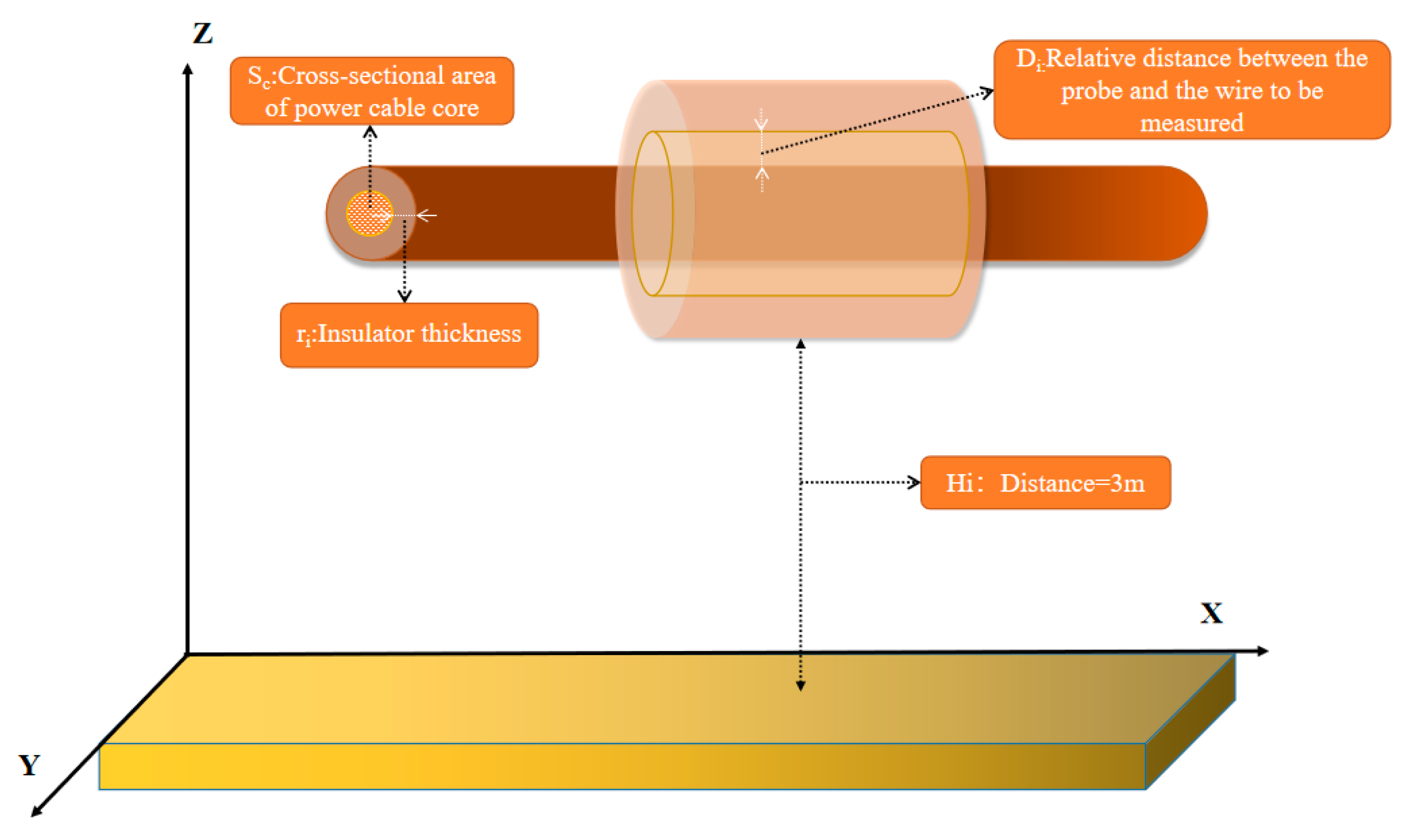
2. Simulation Analysis

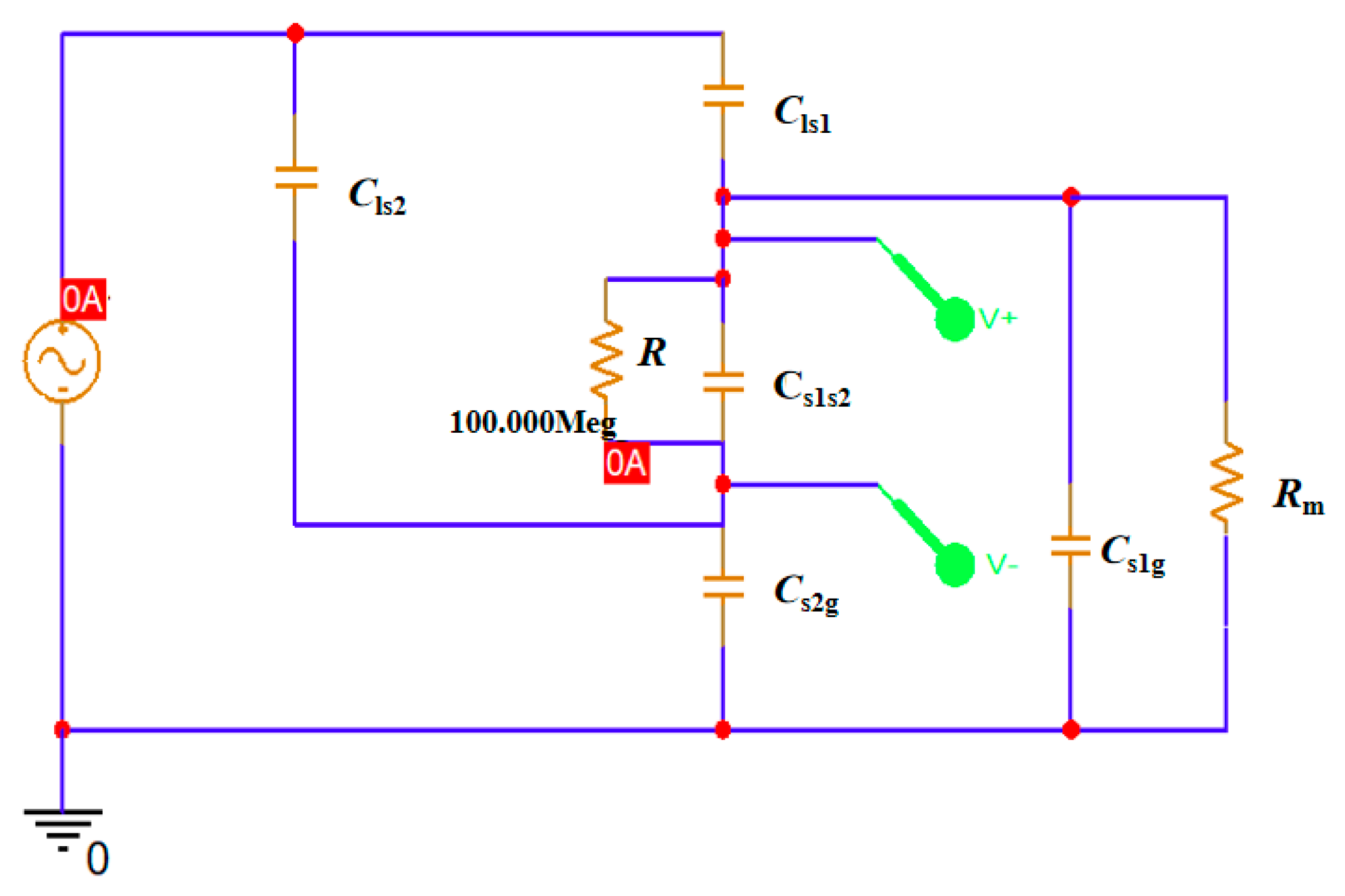
2.1. Five Capacitance Model Simulation Analysis

When the sensor is located in a space with a changing electric field due to the principle of electrostatic induction, an induced charge is generated on the metal electrode. This charge forms a current that flows through the grounding resistor Rm and produces a voltage. The voltage drop is linearly related to the rate of change of the electric field around the conductor under test. Because of the electric field coupling, the sensor induction electrode and the conductor under test are insulated. At the same time, the coupling capacitance reflects the mutual coupling due to the different potentials. Therefore, the collective parametric circuit model of the sensor can be represented in Figure 1. In summary, with non-contact voltage sensors based on the coupling capacitance principle, the sensor gain can fluctuate due to the coupling capacitance’s instabilities, which affects the sensing accuracy. Melanie Schilder proposed the five-capacitance model diagram in the design of a voltage sensor. The purpose was to solve the problem that the sensor’s gain fluctuates due to the instability of the coupling capacitance, which affects the sensing accuracy [21].
From above Figure 1a, it can be seen that the charged wire and the upper plate form the primary capacitance on the high voltage side Cls1, the upper plate and the lower plate form the measurement capacitance Csls2, the lower plate, and the ground form the three capacitance Cs2g, the upper plate to the ground capacitance Cs1g and the lower plate to the wire capacitance Cls2. Based on the equivalent circuit mode Figure 1b, Vi is the input voltage signal in the equivalent circuit diagram, and Vo is the output voltage signal. Cs1s2 is the measurement electrode. The remaining four capacitors, Cls1, Cls2, Cs1g, and Cs2g, are all coupling capacitors, and Rm is the sampling resistor. The transfer function of this circuit can be described as:
G ( s ) = V o V i = s C l R m s C 2 R m + 1
where the equivalent capacitance:
C 1 = C 1 s 1 C 1 s 2 C 1 s 1 C s 1 g C 1 s 1 + C s 1 g + C 1 s 2 + C s 2 g , C 2 = C 1 s 1 C 1 s 2 + C 1 s 1 C s 2 g + C 1 s 2 C s 1 g + C s 1 g C s 2 g C 1 s 1 + C s 1 g + C 1 s 2 + C s 2 g + C s 1 s 2
When the sensor reaches a self-integrating state, the transfer function converts to:
V o V i = C l C 2
From Equation (3), the sensor gain is not only affected by the coupling capacitance Cls1 between the upper pole plate and the wire to be measured, the coupling capacitance Cs2g formed between the lower pole plate and the earth, but also by the stray capacitance Cs1g and Cls2.
According to Equation (3), the gain of the entire sensor probe when detecting voltage is composed of its structural capacitance and other stray capacitances. However, since all capacitances other than the structural capacitance are unknown parameters, the stability of the system gain is also unknown. The gain is usually measured using the fixed scale measurement method, and the output ratio to input gives the gain. However, in the actual measurement, due to the relative position of the charged conductor and the probe, the diameter of the charged conductor itself, the thickness of the insulation skin is not fixed, and other factors appear. These can cause the system gain to be unstable, so measurement accuracy is not guaranteed.
As shown in Figure 2, the variation of S c , r i , and D i within the model will affect the coupling capacitance values. After obtaining the value of each coupling capacitor through COMSOL simulation, the equivalent circuit shown in Figure 1 is built using SPICE. By changing the S c , r i , and D i values in COMSOL, each capacitance value was imported into SPICE for simulation. The degree of impact on the sensor’s measurement accuracy was determined by counting the gain change of the sensor. The circuit simulation diagram is shown in Figure 3.
The simulation results are shown in Table 2, Table 3 and Table 4. The maximum relative error of the gain is 40.01% at a fixed distance. It can be seen that the instability of the coupling capacitor will lead to very large sensor gain instability. Therefore, the same type of sensor in the measurement to be constantly calibrated sensor gain to ensure accurate accuracy.

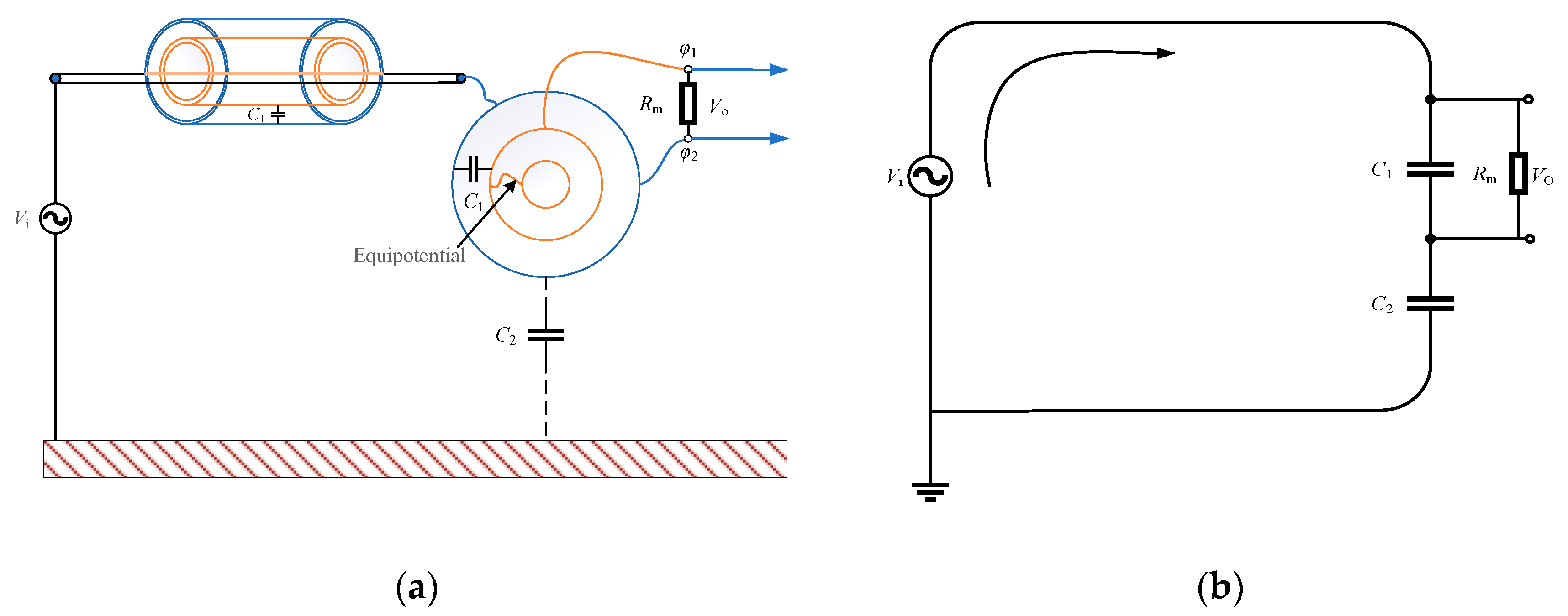
2.2. Principle of Floating Ground Sensor

In contrast to the five-capacitance model described above, the calibration-free voltage measurement method described in this paper is based on a two-capacitance model. It has the advantage that the sensor’s gain is only related to its structural capacitance and the coupling capacitance to the ground. The variables to be controlled are reduced. As shown in Figure 3a, the front-end measurement probe in this paper includes an equipotential electrode to the wire under test and an electrode grounded by coupling to the ground. The inner electrode plate forms an equal potential for measuring the wire. The inner electrode, outer electrode, and insulating medium form a structural capacitance C1, and the floating ground electrode form a capacitance C2 with the natural earth. The equivalent circuit is abstracted in Figure 4a and is shown in Figure 4b.
In Figure 4, C1 is the structural capacitor, C2 is the coupling capacitor, Rm is the sampling resistor, Vi is the line voltage to be measured, and Vo is the output voltage. The transfer function obtained from this equivalent circuit diagram is shown in Equation (4):
V o ( s ) V i ( s ) = s R m C 2 1 + s R m ( C 1 + C 2 )
when s R m ( C 1 + C 2 ) 1 , the transfer function in Equation (3) can be expressed as:
V o V i = C 2 C 1 + C 2
It can be seen from Equation (5) that if the sensor has reached the self-integrating state, the sensor gain is only related to C1 and C2. In order to stabilize the gain of the sensor, it is necessary to ensure that the values of C1 and C2 do not change. The capacitance C1 is a fixed value of the structure. Capacitor C2 is the coupling capacitance formed by the floating grounding plate and the natural earth. Since it is not a fixed value, the stability of its value is crucial to the sensor gain.

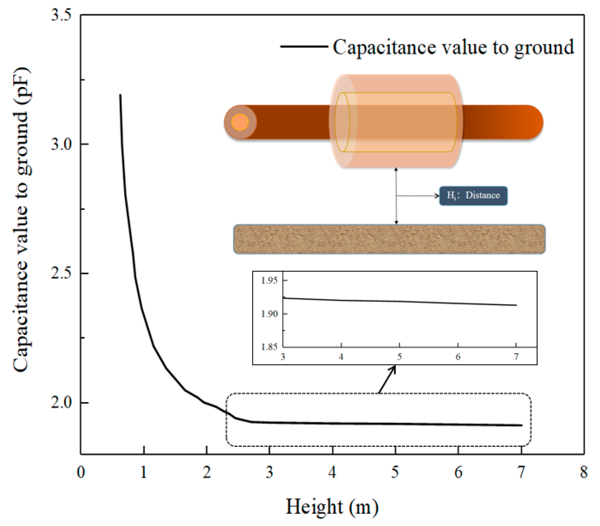
2.3. Simulation Analysis of Coupling Capacitance to Ground

The above transfer function shows that structural and coupling capacitance affect the sensor’s gain. Since C1 is its structural capacitance, its capacitance value will not change. At the same time, C2 couples capacitance to ground. The distance to the ground influences its capacitance value. Therefore, to study its change law, this paper calculates the value of probe-to-earth coupling capacitance at different distances between the probe and the earth using the finite element simulation software COMSOL. The distance between the probe and the earth is increased from 0.1 m to 5 m in steps of 0.1 m. The simulation results are shown in Figure 5.
The simulation results show that the value of the coupling capacitance C2 decreases gradually with the increase in the probe suspension height. However, when the suspension height is greater than 3 m, the trend of decreasing the value of the probe’s distributed capacitance to the ground will slow down. The simulation results show that the coupling capacitance value changes at a rate of only 0.58% between 3 m and 7 m. Therefore, when the sensing probe installation height reaches a specific size, the value of the high-voltage probe to ground distributed capacitance tends to be stable, which in turn ensures the stability of the sensor gain.

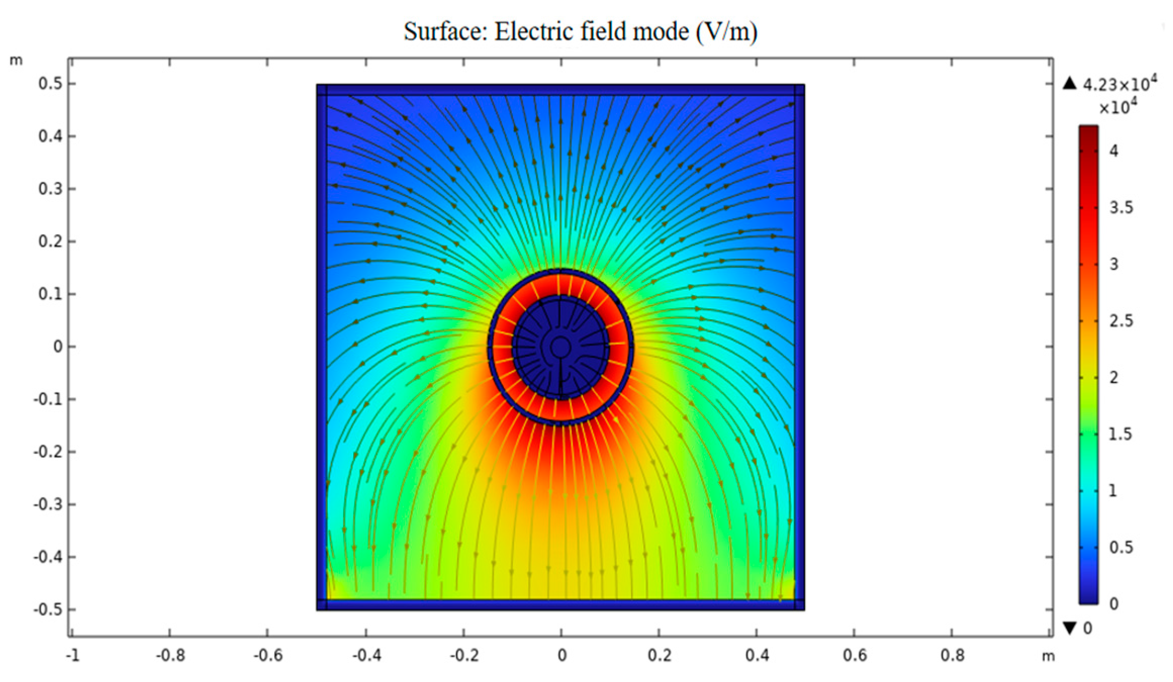
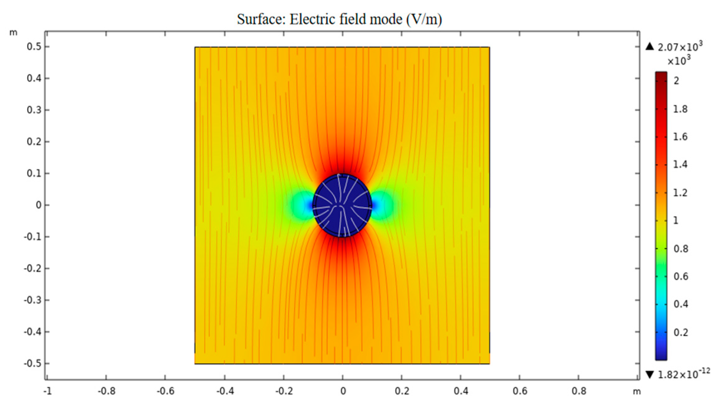
2.4. Electric Field Analysis

By placing an additional probe inside the inner pole plate in direct contact with the metal part of the conductor to be measured, the conductor to be measured is at the same potential as the inner pole plate. The interior of the designed probe is a cavity metal conductor. Therefore, in the electrostatic equilibrium state of the internal electric field, strength is zero. Therefore, adding additional probes will not cause the original electric field distortion. By simulating the electrostatic field at this time through COMSOL, the results are shown in Figure 6.
The floating earth measurement system constructed in this paper is measured from the probe to the back-end circuit, from the opto-isolated probe to the oscilloscope used for signal acquisition without connecting to the natural earth. It is found that the output signal is easily affected by the surrounding electric field during the floating earth measurement. Therefore, the external electric field shielding of the measurement signal needs to be considered.
Taking the Gaussian surface inside the hollow conductor, using Gauss’s theorem, it is obtained that:
ϕ = A Eda = Q ε 0
By Equation (6), it can be seen that the electric flux of the Gaussian surface is equal to the ratio of the charge contained in the Gaussian surface to the constant. From the above simulation, it can be seen that there is no charge inside the cavity, so the electric flux of the Gaussian surface should also be zero, i.e., there is no electric field, since the charges of the conductor are distributed on the outer surface of the conductor. Therefore, outside the Gaussian surface inside the cavity, the change in the outside charge will not affect the Gaussian surface. Therefore, the interior of the hollow conductor is not affected by the external electric field. In this paper, we address this phenomenon by using a hollow cylindrical metal with an insulating skin wrapped around it for signal protection. COMSOL carries out the electric field simulation with the metal pole plate set to the suspension potential and an electric field of 103 kV/m applied in space. The simulation results are shown in Figure 7.
The simulation results show that this method can shield the external electric field’s interference more effectively.

3. Calibration-Free Sensor Design

Under limited resources, a practical design of the calibration-free probe is required to achieve stable sensor gain. Since the sensor gain is determined by its structure capacitance C1 and the ground coupling capacitance C2, it is not very easy to make the sensor reach the state of self-integration by relying on the capacitance value of the sensor probe itself. The protection of the sensor output signal is also critical. We rely on COMSOL software to obtain a coaxial sensor probe Maxwell capacitance under equipotential conditions. The same mechanical processing technology is used to make the output signal protector, which is continuously improved in the experiment. The specific process is shown in Figure 8.

3.1. Stable Sensor Gain

The sensor uses a differential input structure, with electrode one being the potential directly connected to the wire to be measured and electrode two having an unknown floating potential. A differential signal processing circuit converts the potential difference between the two electrodes into a single-ended signal relative to the circuit reference ground potential. The differential signal processing circuit used in this sensor is shown in Figure 9.
The instrumentation amplifier selected for this paper is the AD620, which has a bandwidth of 120 kHz, an input bias current of 1nA, and a supply range of ±2.3 V to ±18 V. Rm is the input impedance of the differential circuit with a size of 10 MΩ. A gain of one is selected because the gain resistor is not connected in the actual connection.
The sensor designed in this paper is intended to measure 50 Hz line voltage at the operating frequency, i.e., the sensor is in self-integrating mode when measuring 50 Hz. This requires that the values of ω h 2 π 50 , R m ( C 1 + C 2 ) satisfy at least Equation (7) for the electric field coupled sensor to operate in the self-integrating mode at operating frequencies.
R m ( C 1 + C 2 ) > 3.18 · 10 3
Considering that the capacitance C1 of the probe structure is determined by the length, the thickness of the pole plate, and the size of the dielectric constant, it is challenging to produce a conventional machining process that can satisfy the large capacitance while making the sensor structure small. Therefore, in the probe design, we decided to ensure that it is in self-accumulation mode during the 50 Hz measurements by using nF-level capacitors in parallel with the probe. The parallel capacitor is a high-voltage ceramic capacitor. The capacitance value is obtained using a TH2840B precision LCR meter with a measurement accuracy of 0.05%, and the capacitance size is 45.86 nF.

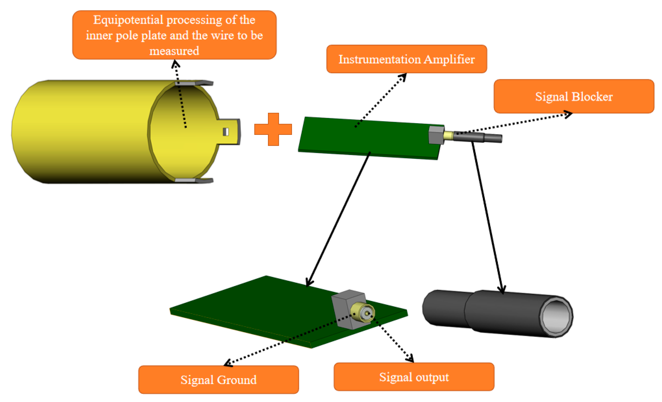
3.2. Signal Shielding Device

In this paper, we use a shield encased in a metal cylinder in the output signal portion of the circuit to shield the external electric field. The overall design of the probe is shown in Figure 10. The front end of the probe is in the shape of a hollow cylinder so that the wire to be measured can be mounted more efficiently. The insulating medium in the middle is a white resin with 1 mm thick copper foil wrapped around the inner and outer sides, the dimensions of which are shown in Table 5. The back end is connected to the differential signal circuit, and the differential signal is transmitted to the remote probe through the signal shield. Finally, a self-powered suspended oscilloscope is used for signal acquisition. A separate battery powers the back-end circuitry to ensure the entire measurement system is floating on the ground.

4. Experimental Design and Analysis of Results

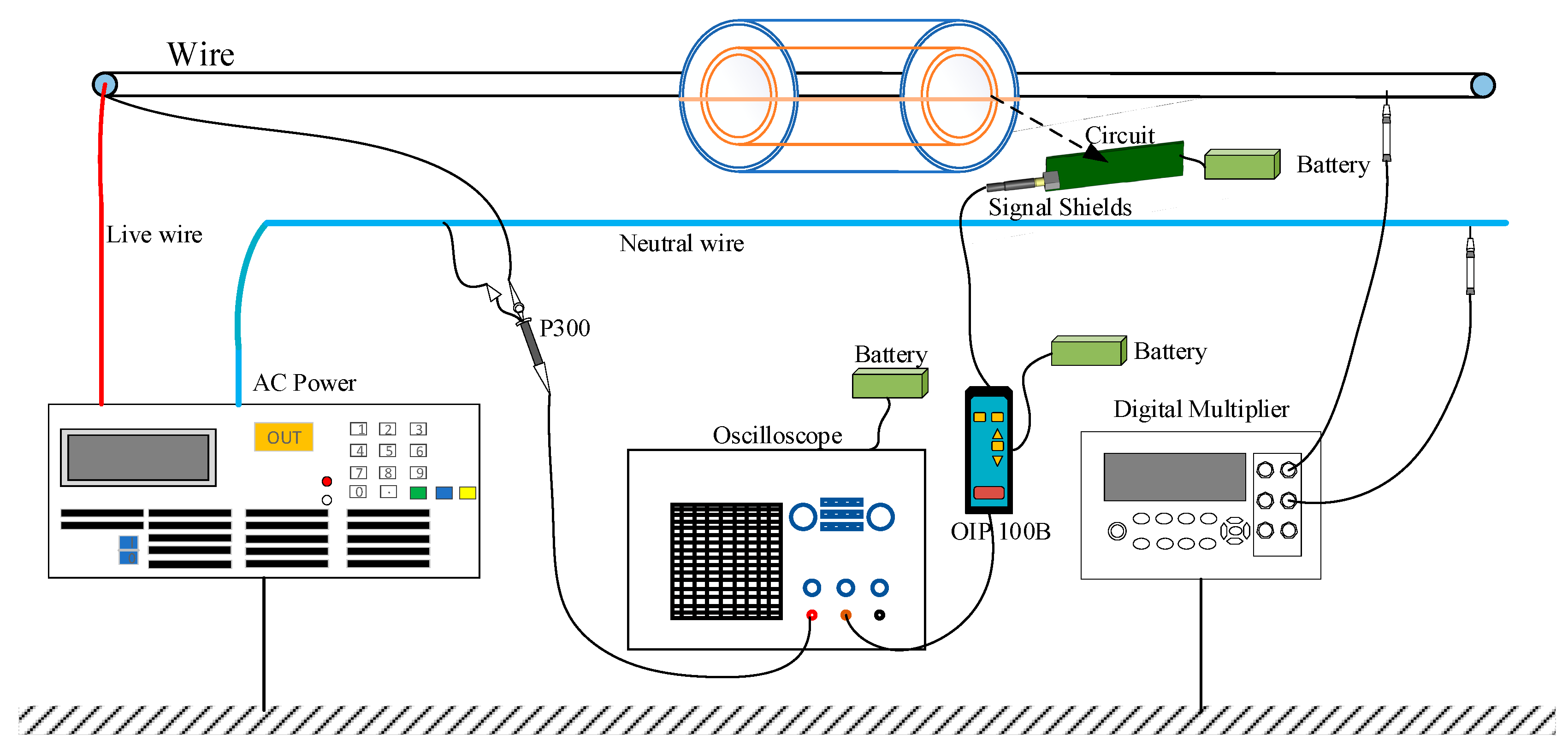
4.1. Design of the Floating Ground Measurement System

The schematic diagram of the grounding system based on spatial capacitive coupling designed in this paper is shown in Figure 11. First, the inner pole plate of the sensing probe is in direct contact with the wire to be measured so that the inner plate and the wire to be measured form an equal potential. Secondly, the external metal plate of the sensing probe is grounded by spatial capacitive coupling to form the coupling capacitance C2, which provides the conditions for constructing a floating ground measurement system. φ1 and φ2 are the measurement electrode potentials for subsequent processing of the circuit, Rm is the input impedance of the back-end circuit, and Vo is the output signal of the sensor, Vo = φ1−φ2. The signal waveform is extracted by the differential circuit, connected to the opto-isolated probe through a shield, and finally observed in a floating-ground oscilloscope. This method of obtaining voltage values by differential based on a floating measurement system is commonly used for signal testing power semiconductor switches such as metal field effect transistors and insulated gate bipolar transistors. It is used to design uninterruptible power supplies, diagnostic motor drives, industrial control equipment, and the testing of power systems and industrial switching power supplies [22].

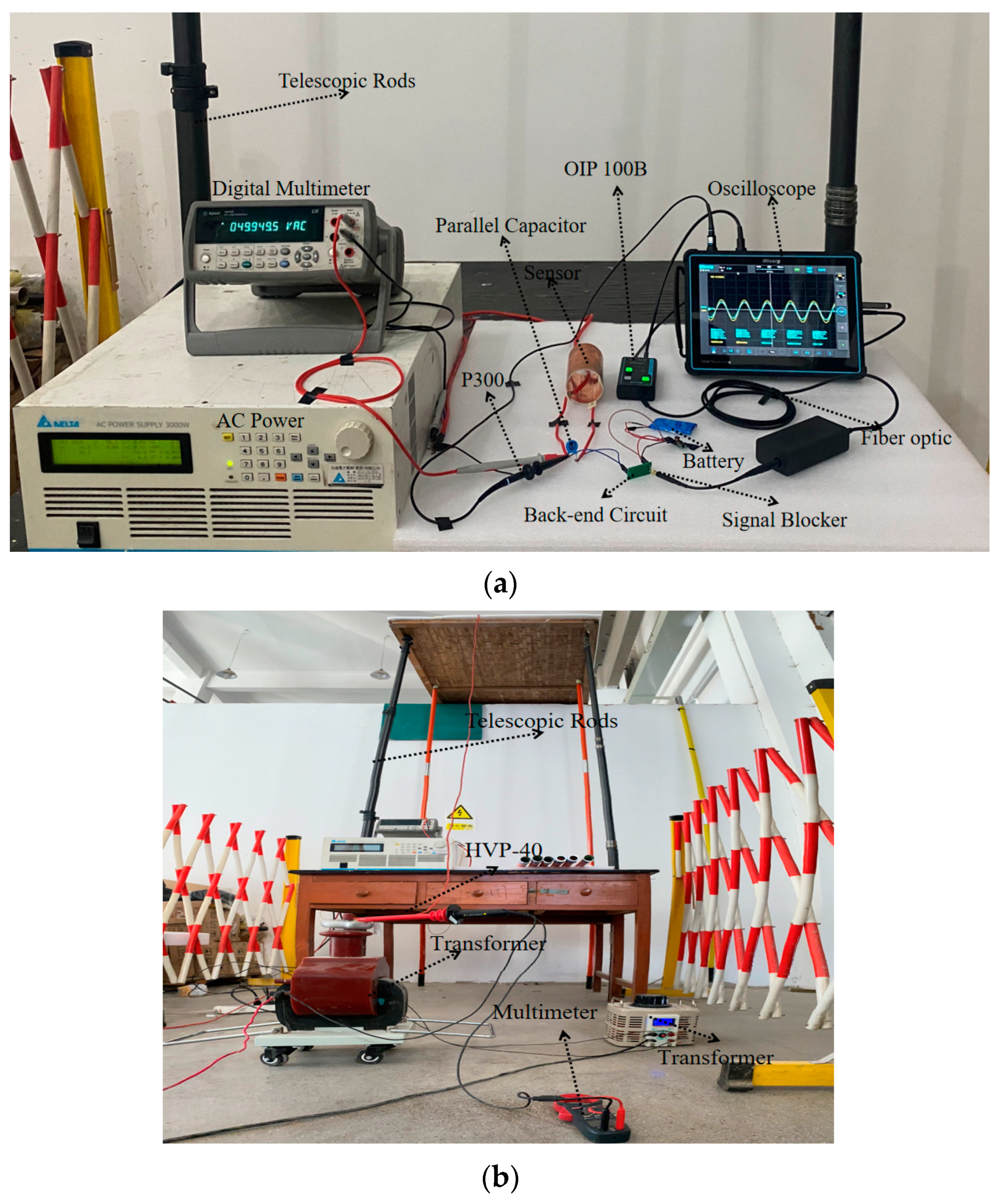
4.2. Construction of the Experimental Platform

In order to verify the feasibility of the floating-ground measurement method, an experimental platform was built under laboratory conditions, and the schematic of the experimental platform is shown in Figure 12. The experimental diagrams are shown in Figure 13a,b. The low voltage source AC voltage came from a DELTA AC power supply of 3000 W, which can provide 30 Hz–1 kHz, 0–300 V effectual AC voltage output. The IHV source was regulated using an indoor power supply connected to a high-stability performance GTB-5/50 IFT transformer, which can output up to 50 kV. An OIP 100 B self-powered opto-isolated probe with 1% accuracy and a 100 MHz measurement band was used to acquire the output signal from the back-end circuit. The output signal was acquired using a TO3004 self-powered isolated oscilloscope with 8-bit resolution and 300 MHz bandwidth. The oscilloscope had a sampling rate of 2 GS/s. An Agilent 34,401A 6½-bit benchtop digital multimeter calibrated the amplitude of the AC output voltage. The high-voltage probe used was PINTEK’s HVP-40. The measurement accuracy of this probe is −5% to 10%. The measurement band is 50 Hz to 60 Hz. The phase was calibrated by direct contact with the source output using the oscilloscope’s 2% accuracy P300 probe. The height of the entire experimental stage was adjusted with a retractable insulated rod.
The line to be measured was passed through the coaxial shield probe, and the two electrodes of the probe were connected to the differential circuit. The differential circuit was connected to a signal shield, and the output signal of the signal shield was connected to a self-powered opto-isolated probe. The optical isolation probe was connected to an oscilloscope, and the oscilloscope observed the real-time waveform. The outer electrode of the coaxial probe was connected to the ground probe of the oscilloscope. Digital multimeter and oscilloscope with a high-voltage differential probe connected to both ends of the voltage source live wire and neutral wire.

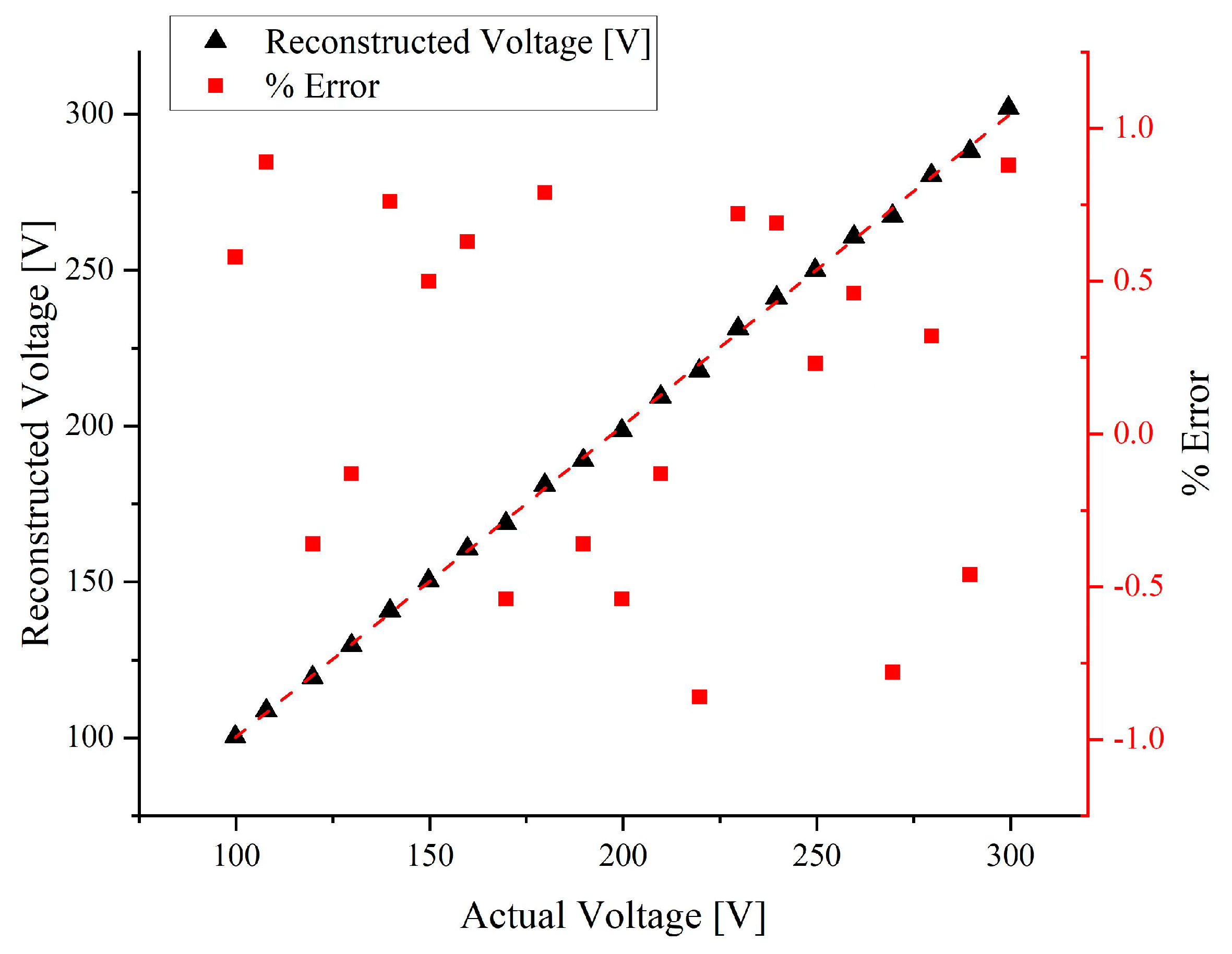
4.3. Low Voltage Amplitude Accuracy Test

The following steps were undertaken on a 3 m high experimental platform. The output range of the AC source was increased from 100 V to 300 V in steps of 10 V. At each step, the observed signal output from the oscilloscope and the output calibration value from the Agilent 34,401A digital multimeter were recorded. The signal output voltage of the maximum error was counted by multiple measurements and converted to the reconstructed voltage. Figure 14 shows the error characteristics of the output voltage measured from the oscilloscope at each step versus the actual voltage output calibrated from the Agilent 34,401A digital multimeter. These error characteristics were calculated using the output voltage from a 50 Hz power supply.
Table 6 gives the measured voltage V m (mV) for the signal processing circuit, as well as the reconstructed signal V r (V) for the maximum error and the actual voltage V a (V) for the output of the digital multimeter. V r is the value of the measured voltage reconstructed using the fitting curve. The gain of the sensor is 21,906. The expression of the fitted curve for the experimental results is y = 0.0466 × −0.1683. (x is the calibration voltage, V; y is the voltage sensor output voltage, mV). The relative ratio error between the voltage source output and the inversion voltage results is shown in Equation (8).
ε = ( V r V a ) V a
As can be seen from Figure 14 and Table 6, the maximum error between the reconstructed voltage and the actual voltage amplitude is 0.89% when measured at 50 Hz.

4.4. High Voltage Amplitude Accuracy Test

The high-voltage amplitude accuracy test was performed on a 3-m-high experimental platform by adjusting the output voltage through a transformer to increase the output range from 600 V to 10 kV. At each step, the observed signal output from the oscilloscope and the calibrated value output from the multimeter were recorded. The reconstructed voltage with the maximum error was tallied. Table 7 shows the output voltage measured from the oscilloscope and the actual voltage output calibrated from the multimeter for each step, this is when using the output voltage from a 50 Hz supply, as well as the maximum measurement error at the time of comparison that was tallied.
It can be seen from Table 7 that the maximum error is 4.68% when the reconstructed voltage is compared with the voltage amplitude measured by the high voltage probe at 50 Hz. This shows that the method is also applicable to high pressure research.

4.5. Phase Accuracy Test

Regarding the calibration of the sensor phase accuracy of the floating earth measurement system, the oscilloscope’s standard probe with 2% accuracy was used to directly contact the power supply for measurement and comparison with the homemade floating earth probe. Since the output signal of the homemade probe used a self-powered opto-isolated probe for signal acquisition, the two probes did not affect each other when compared with the same oscilloscope. The reconstructed voltage and calibration voltage are shown in Figure 15. The red waveform is the real-time waveform of the standard probe that comes with the oscilloscope, and the black waveform is the reconstructed waveform after using linear fitting. After several comparisons, the results show that the phase relative error is within 0.68°. In summary, the sensor prototype has steady-state characteristics with small amplitude and phase shifts when measuring 50 Hz AC.

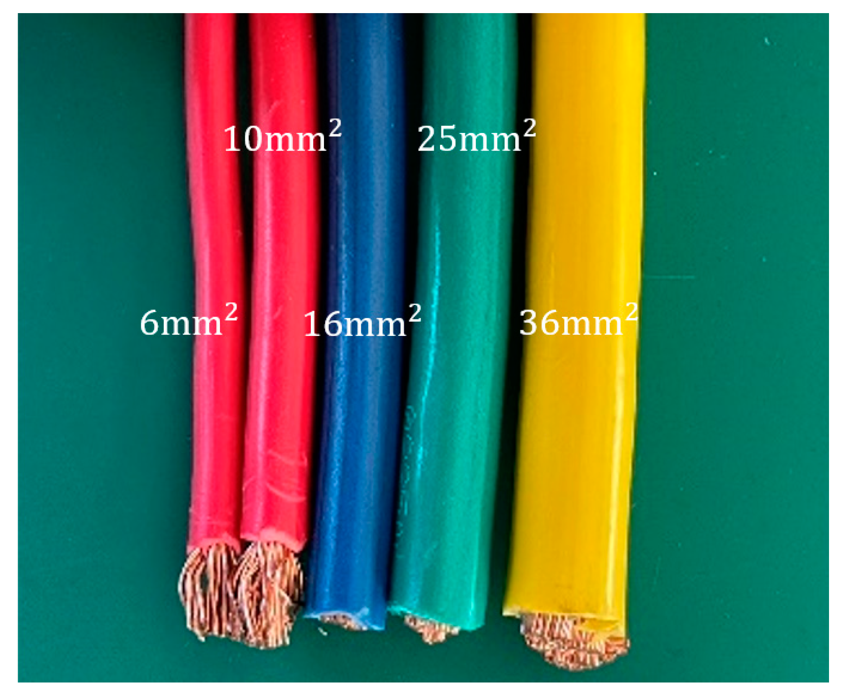
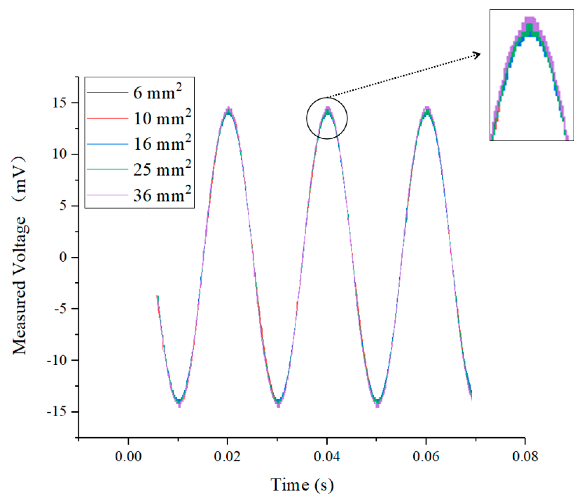
4.6. Scene Adaptability Testing

In order to verify the gain stability of the method at different heights, the distance adjustment was performed by raising the insulated pole. The raised distances are 1 m, 2 m, 3 m, 4 m, and 5 m, in order. The AC source output voltage is set to 100 V, 200 V, and 300 V.
Table 8 and Figure 16 show that the maximum error after the floating ground measurement platform height reaches 3 m is only 0.88%, and the sensor gain will reach stability. Therefore, this method has the advantage of self-calibration when performing voltage measurements on overhead transmission lines. The sensor gain can be calibrated on the line before use.
In addition, amplitude tests were conducted on various types of conductors in this paper. Several conductors that are more common in the national standard were selected. They are standard conductors with cross-sectional areas of 6 mm2, 10 mm2, 16 mm2, 25 mm2, and 36 mm2, as shown in Figure 17 [23]. The purpose is to verify that the sensor gain is affected when measuring different wire sizes and insulation thicknesses. The test was performed by replacing the above types of conductors in turn, and all the conductors were randomly placed in the sensing probe without special fixation, and the waveforms are shown in Figure 18.
The experimental results show that the maximum difference between the measured values of the five wire diameters does not exceed 0.52%. It can be seen that the floating ground voltage measurement method based on equipotential is not affected by different wire diameters and different placements.

5. Conclusions

In this paper, a floating grounded AC voltage measurement system based on equipotential and differential structures is constructed. When compared with other AC voltage measurement methods, the installation location does not limit the installation scheme based on whether the measurement equipment is grounded. Complex insulation issues do not need to be considered. Since the internal pole plate is directly connected to the conductor, the effects of wire diameter, insulation thickness, and the relative position of the conductor under test are significantly mitigated, making the sensing probe designed by this method self-calibrating.
  • A novel voltage measurement scheme is proposed, and an equivalent theoretical model of dual capacitance is developed.
  • The feasibility of the floating-ground measurement is verified using the equipotential and differential circuit methods. The maximum relative error of the voltage amplitude is 0.89%, and the phase difference is 0.68° for the voltage range (100 V–300 V) of the IFT voltage test. The maximum relative error of the voltage amplitude in the voltage range (600 V–10 kV) for the 50 Hz working frequency voltage test is 4.48%.
  • The floating ground measurement method developed for this sensor has an amplitude accuracy error of only 0.88% after a specific height, a maximum difference of 0.52% for multiple line tests, and a stable sensor gain stability that allows for the self-calibration of the sensor.
  • The sensor can be used in the future for voltage measurements on high-voltage transmission lines because of its high gain and the fact that it does not require consideration of insulation.

Author Contributions

The idea of this work was proposed by W.L., W.Z. and L.Y.; W.Z., P.Y., J.L., Y.Z. and L.Y. performed the experiments and analyzed the results. L.Y. wrote the paper. All authors have read and agreed to the published version of the manuscript.

Funding

“Internet of Things Intelligent Sensing Terminal Platform System and Application Verification Project” (2018YFB2100100), “Research and development of new smart sensor technology to promote the development of green energy” (202104BN050011), and “Research and development of key technologies for conformal implantation of new intelligent power sensing for power grid main equipment” (YNKJXM20210075) funding.

Acknowledgments

The authors will thank the reviewers and editors for the revision of this paper and the suggestions of English editors, which will help improve the English expression, readability, and quality of the article. The author thanked X.T. and W.Z. for their support and contribution to this study.

Conflicts of Interest

The authors declare no conflict of interest.

References

  1. Yang, Q.; Sun, S.; Sima, S.; Luo, M. Research progress of advanced voltage and current sensing methods for smart grids. High Volt. Technol. 2019, 45, 349–367. [Google Scholar] [CrossRef]
  2. Gholizadeh-Roshanagh, R.; Zare, K. Electric power distribution system expansion planning considering cost elasticity of demand. IET Gener. Transm. Distrib. 2019, 13, 5229–5236. [Google Scholar] [CrossRef]
  3. Tan, Q.; Zhang, W.; Tan, X.; Yang, L.; Ren, Y.; Hu, Y. Design of Open-Ended Structure Wideband PCB Rogowski Coil Based on New Winding Method. Electronics 2022, 11, 381. [Google Scholar] [CrossRef]
  4. Ma, X.; Guo, Y.; Chen, X.; Xiang, Y.; Chen, K.-L. Impact of Coreless Current Transformer Position on Current Measurement. IEEE Trans. Instrum. Meas. 2019, 68, 3801–3809. [Google Scholar] [CrossRef]
  5. Crescentini, M.; Marchesi, M.; Romani, A.; Tartagni, M.; Traverso, P.A. A Broadband, On-Chip Sensor Based on Hall Effect for Current Measurements in Smart Power Circuits. IEEE Trans. Instrum. Meas. 2018, 67, 1470–1485. [Google Scholar] [CrossRef]
  6. Xuan, H.; Wen, C.; Song, Y.; Wei, X. Fault detection and analysis of capacitive components of capacitive voltage transformer. E3S Web Conf. 2020, 218, 01001. [Google Scholar] [CrossRef]
  7. Dong, W.; Sun, Z.; Gao, C.; He, Z.; Zha, K. Research and Experiment Verification of the Shielding Effect of a 1000kV Equipotential Shielding Capacitor Voltage Transformer in Consideration of Surface Leakage Current. IEEE Trans. Power Deliv. 2022, 1–8. [Google Scholar] [CrossRef]
  8. Tajdinian, M.; Allahbakhshi, M.; Behdani, B.; Behi, D.; Goodarzi, A. Probabilistic framework for vulnerability analysis of coupling capacitor voltage transformer to ferroresonance phenomenon. IET Sci. Meas. Technol. 2020, 14, 344–351. [Google Scholar] [CrossRef]
  9. Ding, X.; Yang, K.; Wang, W.; Liu, B.; Wang, X.; Zhang, J.; Li, D. Ferro-Resonance Analysis of Capacitor Voltage Transformer with Fast Saturation Damper. Energies 2022, 15, 2791. [Google Scholar] [CrossRef]
  10. Zhang, Y.; Zhang, C.; Li, H.; Chen, Q. An online detection method for capacitor voltage transformer with excessive measurement error based on multi-source heterogeneous data fusion. Measurement 2022, 187, 110262. [Google Scholar] [CrossRef]
  11. Lu, P.; Wang, W.; Yu, Q.; Fan, B.; Liu, P.; Wang, F.; Zeng, X. Permanent Single-Line-to-Ground Fault Removal Method for Ferro-Resonance Avoidance in Neutral Ungrounded Distribution Network. IEEE Access 2022, 10, 53724–53734. [Google Scholar] [CrossRef]
  12. Yablokov, A.; Kabakov, P.; Gotovkina, E. Investigation of the Current Conversion Error of Rogowski Coil in a Wide Temperature Range. In Proceedings of the 2022 International Ural Conference on Electrical Power Engineering (UralCon), Magnitogorsk, Russia, 23–25 September 2022; pp. 307–312. [Google Scholar] [CrossRef]
  13. Rehman, A.U.; Lie, T.T.; Valles, B.; Tito, S.R. Event-detection algorithms for low sampling nonintrusive load monitoring systems basedon low complexity statisticalfeatures. IEEE Trans. Instrum. Meas. 2020, 69, 751–759. [Google Scholar] [CrossRef]
  14. Zhao, P.; Wang, J.; Wang, Q.; Xiao, Q.; Zhang, R.; Ou, S.; Tao, Y. Simulation, Design, and Test of a Dual-Differential D-Dot Overvoltage Sensor Based on the Field-Circuit Coupling Method. Sensors 2019, 19, 3413. [Google Scholar] [CrossRef] [PubMed]
  15. Wang, L.; Zhang, W.; Tan, X.; Chen, W.; Liang, S.; Suo, C. Research and Experiments on an External Miniaturized VFTO Measurement System. Sensors 2019, 20, 244. [Google Scholar] [CrossRef] [PubMed]
  16. Wang, J.; Li, X.; Wang, Q.; Zhong, L.; Zhu, X. Research on transmission line voltage measurement method based on Gauss-Kronrod integral algorithm(Article). Meas. Sci. Technol. 2020, 31, 085103. [Google Scholar] [CrossRef]
  17. Xiao, D.P.; Xie, Y.T.; Ma, Q.C. Non-contact voltage measurement of three-phase overhead transmission line based on electric field inverse calculation. IET Gener. Transm. Distrib. 2018, 12, 2952–2957. [Google Scholar] [CrossRef]
  18. Epperson, D.; Rodriguez, R. Proving Unit for Non-Contact Voltage Measurement Systems. EP Patent EP3321697B1, 10 November 2017. [Google Scholar]
  19. Shenil, P.S.; George, B. Evaluation of a digitizer designed to inter-face a non-intrusive AC voltage measurement probe. IEEE Sens. J. 2020, 20, 5606–5614. [Google Scholar] [CrossRef]
  20. Steuer, R.; Ringsrud, P.A.; Worones, J.; Radda, P.; Schmitzer, C.K. Non-Contact Voltage Measurement System Using Reference Signal. U.S. Patent 10 139 435,B2, 27 November 2018. [Google Scholar]
  21. Schilder, M. Wideband Modelling of Capacitive Voltage Sensors for Open-Air Transmission Line Applications. Ph.D. Thesis, Stellenbosch University, Stellenbosch, South Africa, 2002. [Google Scholar]
  22. Soto-Camacho, R.; Vergara-Limon, S.; Vargas-Treviño, M.A.D.; Paic, G.; López-Gómez, J.; Vargas-Treviño, M.; Gutierrez-Gutierrez, J.; Martínez-Solis, F.; Patiño-Salazar, M.E.; Velázquez-Aguilar, V.M. A Current Monitor System in High-Voltage Applications in a Range from Picoamps to Microamps. Electronics 2021, 10, 164. [Google Scholar] [CrossRef]
  23. JB/T 8734.2-2012; Polyvinyl Chloride Insulated Cables and Wires with Rated Voltage 450/750v and Below Part 2: Cables and Wires for Fixed Wiring. Ministry of Industry and Information Technology of the People’s Republic of China: Beijing, China, 2012.
Figure 1. Five capacitance model. (a) Principal diagram of five capacitance; (b) Equivalent circuit diagram of five capacitance model.
Electronics 12 00814 g001
Figure 2. Simulation model schematic.
Electronics 12 00814 g002
Figure 3. Circuit simulation diagram.
Electronics 12 00814 g003
Figure 4. Two capacitance model. (a) Principal diagram of two capacitance model; (b) Equivalent circuit diagram of two capacitance model.
Electronics 12 00814 g004
Figure 5. Coupling capacitance simulation results.
Electronics 12 00814 g005
Figure 6. Electric field simulation diagram.
Electronics 12 00814 g006
Figure 7. Electric field shielding simulation diagram.
Electronics 12 00814 g007
Figure 8. Flow chart.
Electronics 12 00814 g008
Figure 9. Differential signal processing diagram.
Electronics 12 00814 g009
Figure 10. Simulation results of multi-wire diameter and multi-position coupling capacitance.
Electronics 12 00814 g010
Figure 11. Schematic diagram of the grounding system with spatial capacitive coupling.
Electronics 12 00814 g011
Figure 12. Experimental schematic.
Electronics 12 00814 g012
Figure 13. Schematic diagram of the experimental platform. (a) Low Voltage Test Platform; (b) High Voltage Test Platform.
Electronics 12 00814 g013
Figure 14. Error characteristics of the actual output voltage versus the probe output.
Electronics 12 00814 g014
Figure 15. Comparison of the reconstructed voltage of the homemade sensor and the measured output of the standard probe.
Electronics 12 00814 g015
Figure 16. Experimental comparison chart for different heights.
Electronics 12 00814 g016
Figure 17. Different types of wires to be tested.
Electronics 12 00814 g017
Figure 18. Multi-line warp test comparison chart.
Electronics 12 00814 g018
Table 1. Comparison of voltage measurement methods.
SchemeReferenceMethod UsedMain LimitationsThe Technical Gaps Solved in This Paper
CVT, VT[1,6,7,8,9,10,11,12]Series capacitor voltage division and Magnetic induction principle proportional voltage conversion1. Effective grounding is needed, and the insulation performance of the equipment is required.
2. Limited installation location.
1. There is no need for grounding measurement, but it can ensure high measurement accuracy.
2. For various types of wires, the measurement can also ensure a higher measurement accuracy.
3. In the voltage test, there is no specific limit on the installation location.
External Miniaturized VFTO Measurement System[15]Electric field coupling1.The measurement accuracy for a variety of wires is not high.
2. Effective grounding is needed, and the insulation performance of the equipment is required.
Non-Contact line voltage sensor[17]
Dual-slope
FFT Magnitude
[19,20]Electric field coupling andTwo frequency approach
Body capacitance[18]Electric field coupling
Table 2. Change the measurement thickness.
Parameters123456789
Insulation thickness ri0 mm0.5 mm1 mm1.5 mm2 mm2.5 mm3 mm3.5 mm4 mm
Sensor gain330.25322.78318.41315.59310.70308.66305.93302.48 300.76
Table 3. Change the radius of the measurement conductor.
Parameters123456789
Wire Diameter Sc0.5 mm1 mm1.5 mm2 mm2.5 mm3 mm3.5 mm4 mm4.5 mm
Sensor gain359.71347.92330.25330.25321.63314.46309.02301.66296.71
Table 4. Change the position of the measurement conductor with respect to the probe.
Parameters123456789
Relative distance Di0 mm1 mm2 mm3 mm4 mm5 mm6 mm7 mm8 mm
Sensor gain 318.41318.02317.95317.55311.81305.77297.63282.27256.91
Table 5. Capacitor specific dimensions.
ParametersValues
Length 100 mm
Internal insulation radius 25 mm
External insulation radius27 mm
Capacitance value128 pF
Table 6. Low voltage test results.
Actual Voltage
(V)
Measured Voltage
(mV)
Reconstructed Voltage for Maximum Error
(V)
% Error
99.854.50100.430.58
107.844.89108.800.89
119.835.38119.39−0.36
129.835.86129.66−0.13
139.776.38140.830.76
149.766.83150.510.50
159.757.31160.760.63
169.737.68168.81−0.54
179.738.26181.150.79
189.678.62188.99−0.36
199.669.07198.58−0.54
209.649.57209.36−0.13
219.639.96217.74−0.86
229.6310.59231.290.72
239.5611.06241.220.69
249.5511.47250.130.23
259.5411.97260.740.46
269.5312.28267.42−0.78
279.5112.88280.400.32
289.5113.24288.17−0.46
299.4413.89302.080.88
Table 7. Reconfiguration voltage and error.
Actual Voltage(V)Measured Voltage (mV)Reconstructed Voltage (V)% Error
67432.67704.68 4.55%
87242.37912.84 4.68%
125460.141294.17 3.20%
168981.361749.53 3.58%
2243106.132281.08 1.70%
2480118.152539.02 2.38%
2754122.892640.74 −4.11%
3659176.973801.25 3.89%
3819179.623858.12 1.02%
4659219.474713.27 1.16%
4922238.75125.93 4.14%
5427259.185565.41 2.55%
5851277.95967.13 1.98%
6679323.46943.53 3.96%
6872366.27861.98 1.44%
7750389.28355.54 2.69%
8842421.989058.98 2.45%
9762449.729654.26 −1.10%
10,210485.5910,424.00 2.10%
Table 8. Error characteristics of actual output voltage and reconstructed voltage at different heights.
Height (m)Actual Voltage (V)Measured Voltage (mV)Reconstructed Voltage
(V)
% Error
199.855.03 111.4811.65
199.6610.26 223.7412.06
299.4415.44 334.9211.85
299.854.60 102.232.39
199.669.33 203.892.12
299.4414.02 304.441.67
399.854.51 100.430.58
199.669.09 198.58−0.54
299.4413.91 302.080.88
499.854.46 99.22−0.63
199.669.07 198.15−0.76
299.4413.71 297.72−0.57
599.854.47 99.44−0.41
199.669.09 198.58−0.54
299.4413.70 297.50−0.65
Disclaimer/Publisher’s Note: The statements, opinions and data contained in all publications are solely those of the individual author(s) and contributor(s) and not of MDPI and/or the editor(s). MDPI and/or the editor(s) disclaim responsibility for any injury to people or property resulting from any ideas, methods, instructions or products referred to in the content.

