1. Introduction
Time jitter, which is generally regarded as the time error when the timing event of a signal deviates from its expected or desirable occurrence time, is one of the main parameters for estimating the performance of digital optical signals and is of fundamental importance for optical communications and cloud computing [
1,
2]. Conventionally, both asynchronous sampling and synchronous sampling techniques are used to monitor the quality of optical signals [
3,
4,
5,
6]. In general, timing extraction is necessary for the synchronous sampling-based signal quality monitoring system, whereas asynchronous sampling dispenses with timing extraction. With the explosion of information and the development of round-the-clock information transmission services, online monitoring of optical signal jitter characteristics is of growing importance. Eye diagram analysis, which can be categorized as a synchronous sampling-based time-domain signal monitoring technique, is one of the most popular real-time jitter characterization techniques [
5,
6]. In general, time jitter analysis using eye diagrams can be broken down into two steps.
The first step is to sample and quantize the optical signal to build an eye diagram. The sampling of the optical signal can be achieved using both electronic [
7] and photonic [
8,
9,
10,
11,
12] techniques. For electrical sampling, the optical signal should be photoelectrically converted to an electrical signal via a wide-band photodetector (PD) and electrically sampled by a high-speed sample-and-hold circuit. However, increasing data rates present implementation challenges for high-speed electronics. One solution is optical sampling, which enables a high temporal resolution for the sampling due to the short optical sampling pulse which can be obtained by a mode-locked laser [
8], or nonlinear photonics such as the second-order nonlinear effect [
9,
10] in nonlinear crystals, or periodically poled LiNbO
3 and third-order nonlinear effects [
11,
12] (Kerr effect) in semiconductor optical amplifiers (SOAs) or optical fibers. Usually, the generated pulses are as short as around 1 ps, and repetition rates as low as around kilohertz to megahertz. However, it should be noted that although the temporal resolution is increased, the short pulses impose higher quantization efficiency requirements on quantization devices, and the low repetition rates increase the eye diagram formation time. In order to increase the quantization efficiency of low-speed quantization devices and meet the increasing requirements of real-time time jitter monitoring, a delicate balance between temporal resolution and sampling rate is required for the sampling signal. In other words, the sampling pulse generator should have a modest pulse width and repetition rate to accommodate the optical signal data rate. In addition, the repetition rate should be tunable to match optical signals with different data rates.
The second step is to plot the jitter histogram according to the eye diagram to extract the total jitter (TJ), which consists of bounded deterministic jitter (DJ) and unbounded random jitter (RJ) components [
13]. Recently, many jitter decomposition techniques [
14,
15,
16,
17] have been proposed to extract different jitters. For example, Point Net [
15], in which the two coordinates of the jitter histogram are used as point cloud data for training, has shown good performance on jitter decomposition. The dual-Dirac model is used to further improve decomposition accuracy [
16]. In addition, the dual-Dirac model is also used to assist in improving the accuracy of artificial neural network-based jitter decomposition techniques [
17]. It can be concluded that the dual-Dirac model shows an extremely high capability to perform jitter decomposition precisely according to the jitter histogram.
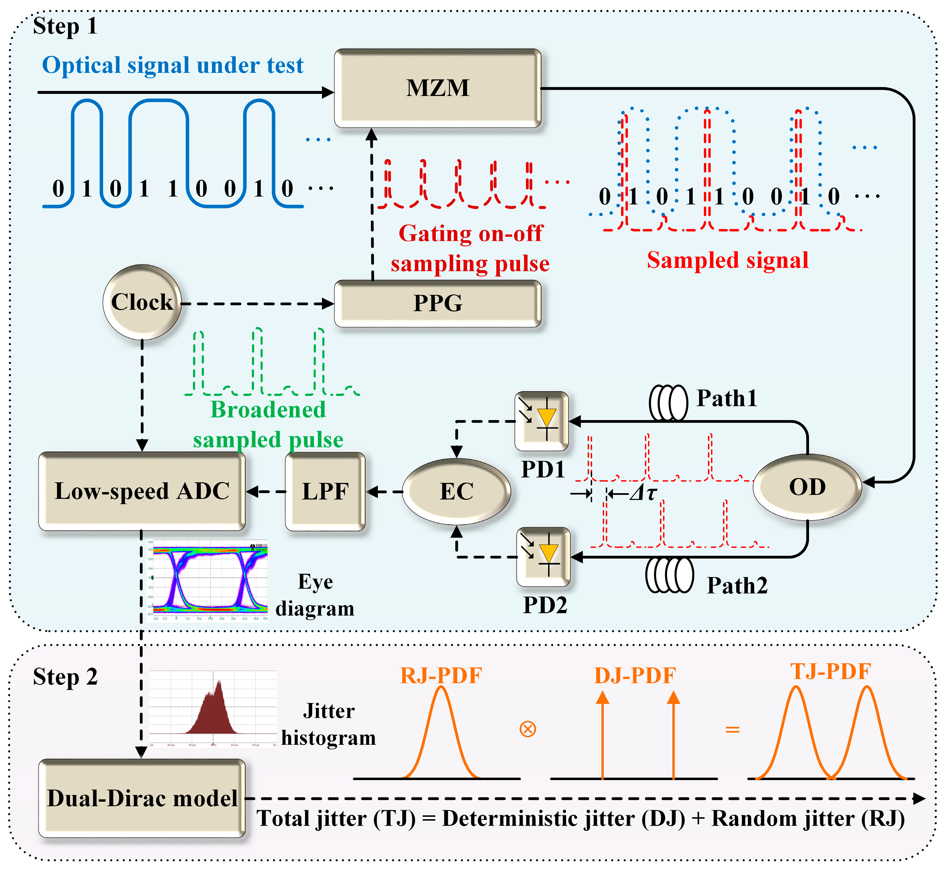
In this paper, a time jitter analysis method that can be carried out in two steps is developed based on gated on-off optical sampling and dual-Dirac modeling. In the first step, the optical signal is sampled through an optical sampling pulse train, and an eye diagram is obtained based on the sampled data. In the second step, a jitter histogram is achieved based on the eye diagram, and the dual-Dirac model is used to implement the time jitter decomposition. The optical sampling pulse train is achieved by the gating on-off modulation of a Mach-Zehnder modulator (MZM). Due to the tunable gigahertz-level repetition rate and tens of ps pulse width of the sampling pulse, the proposed jitter analysis system shows a delicate balance between temporal resolution and sampling rate for a 2.5 GHz optical signal; thus, a real-time jitter analysis can be achieved without using a quantization device with extremely high operation frequency. At the same time, the use of the dual-Dirac model ensures accurate time jitter decomposition. A 21.5 ps TJ, including a 13.2 ps DJ and an 8.3 ps RJ, is measured for a 2.5 GHz optical signal using the proposed time jitter analysis method. The results are verified by a commercial real-time oscilloscope.
2. Theory of Optical Sampling and Time Jitter
Figure 1 shows the schematic diagram of the proposed time jitter analysis method for an optical signal. As can be seen, the jitter analysis can be implemented using two steps. The first step is to obtain an eye diagram using gating on-off optical sampling. The optical signal under test, which can be coupled out from an optical transmission link or source with negligible impact on the signal transmission, is sent to an MZM, where the optical signal is optically sampled by gating on-off sampling pulses from a pulse pattern generator (PPG). In particular, the repetition rate 1/
T and pulse width
W = 1/(
NT) of the optical sampling pulse train can be flexibly adjusted by tuning the PPG, where
T is the period of the sampling pulse, and
N is a positive integer. The sampled optical signal is then transmitted to an optical divider, where the signal is divided into two paths. The two optical signals, which have the same pulse width, repetition rate, and amplitude, are transmitted through two optical fibers with a time delay difference of
Δτ ≈
W and detected by two photodetectors (PDs). The two detected signals are combined into one path via an electrical coupler (EC) and filtered by a low-pass filter (LPF). Consequently, the sampled pulse is broadened to match the sample rate of a low-speed electrical analog-to-digital converter (ADC), where the broadened sampling pulse is quantified with the same rate as the sampling pulse, and an eye diagram is obtained based on the sampled data. Due to the excellent match between the pulse width of the broadened sampling pulse and the hold time of the low-speed sample-and-hold circuit, the quantization efficiency of the ADC is improved. In addition, the ADC and the PPG are synchronized through a clock generator to ensure the quantization rate of the ADC matches the sampling rate of the sampling optical pulse train.
The second step is to implement the time jitter decomposition according to the eye diagram obtained in step 1. Firstly, a time jitter histogram is obtained based on the eye diagram, and a dual-Dirac model [
18] is used to realize the jitter decomposition. As shown in
Figure 1, the dual-Dirac model is realized based on the statistical-domain jitter probability distribution function (PDF). The TJ-PDF in the dual-Dirac model is the convolution of the RJ-PDF and the DJ-PDF. The TJ-PDF can then be given by [
18]
where
t is the time shift relative to the ideal time, and PDF
TJ(
t) and PDF
DJ(
t) denote the RJ-PDF and DJ-PDF, respectively.
RJ is unbounded in nature and follows a normal or Gaussian distribution. Thus, the RJ-PDF can be described using a normal distribution function as [
18]
where
σ is the standard deviation of the normal distribution.
DJ is bounded and can be described using two Dirac delta functions as [
18]
where
δ( ) is the Dirac delta function,
μL and
μR are the deterministic time positions, and the DJ can be presented as |
μR −
μL|.
According to Equations (2) and (3), Equation (1) is rewritten as [
18]
Then the TJ can be given as the sum of the RJ and DJ [
18].
3. Results and Discussion
A proof-of-concept experiment was carried out based on the setup shown in
Figure 1. The optical signal under test with an optical power of 0 dBm was generated from a 2.5 G optical transmitter (CETC-2.5G-SFP). The MZM (CETC-40) has a 3 dB bandwidth of about 40 GHz. Both the PDs (Kang Guan KG-PD-10G) have a 3 dB bandwidth of around 10 GHz and a photoresponsivity of 0.8 A/W. The 3 dB bandwidths of the LPF (Mini-Circuits VLP-41) and EC (Mini-Circuits ZFRSC-123-S+) are 4 and 12 GHz, respectively. The ADC (AcelaMicro) has a maximum sampling rate of 2 Gsps, a 10-bit quantization resolution, and a bandwidth of 4 GHz. A PPG (Anritsu MU183021A) with a 32G-bit/s rate is used to gate the MZM on-off.
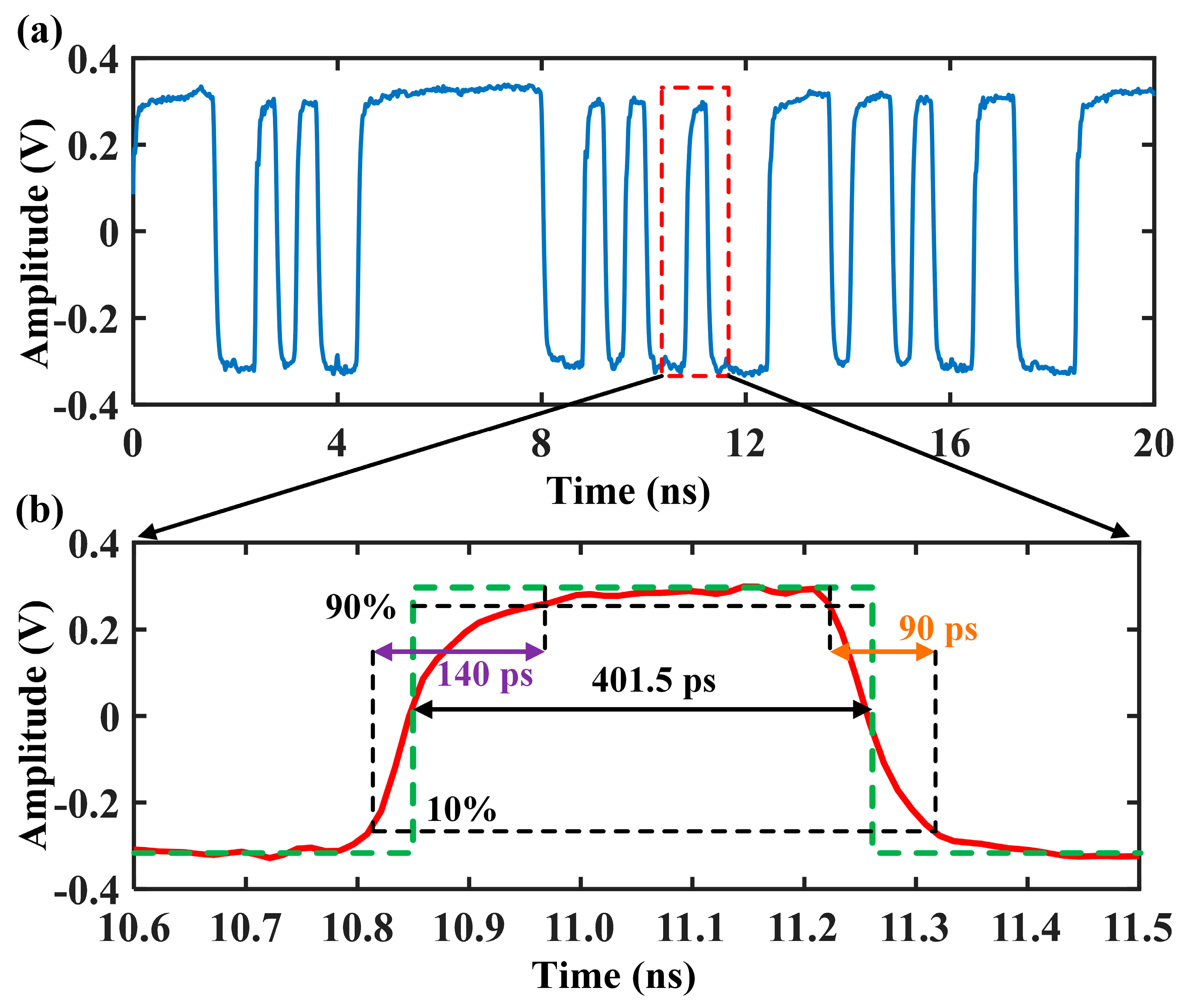
Figure 2a shows the measured optical signal (CETC-2.5G-SFP), which was optoelectronically converted through a photodetector and measured by a commercial oscilloscope (Teledyne Lecroy SDA 820Zi-B) with a sampling rate of 80 GS/s, generated from the 2.5 G optical transmitter at a random 20 ns period. It can be seen that the optical signal under test is a random non-return-to-zero (NRZ) code.
Figure 2b shows the zoom-in view of the measured optical signal measured from 10.6 to 11.5 ps. As can be seen, the optical signal has a bit time of about 401.5 ps, a rise time of about 140 ps, and a fall time of around 90 ps when the thresholds are 10% and 90% of the amplitude.
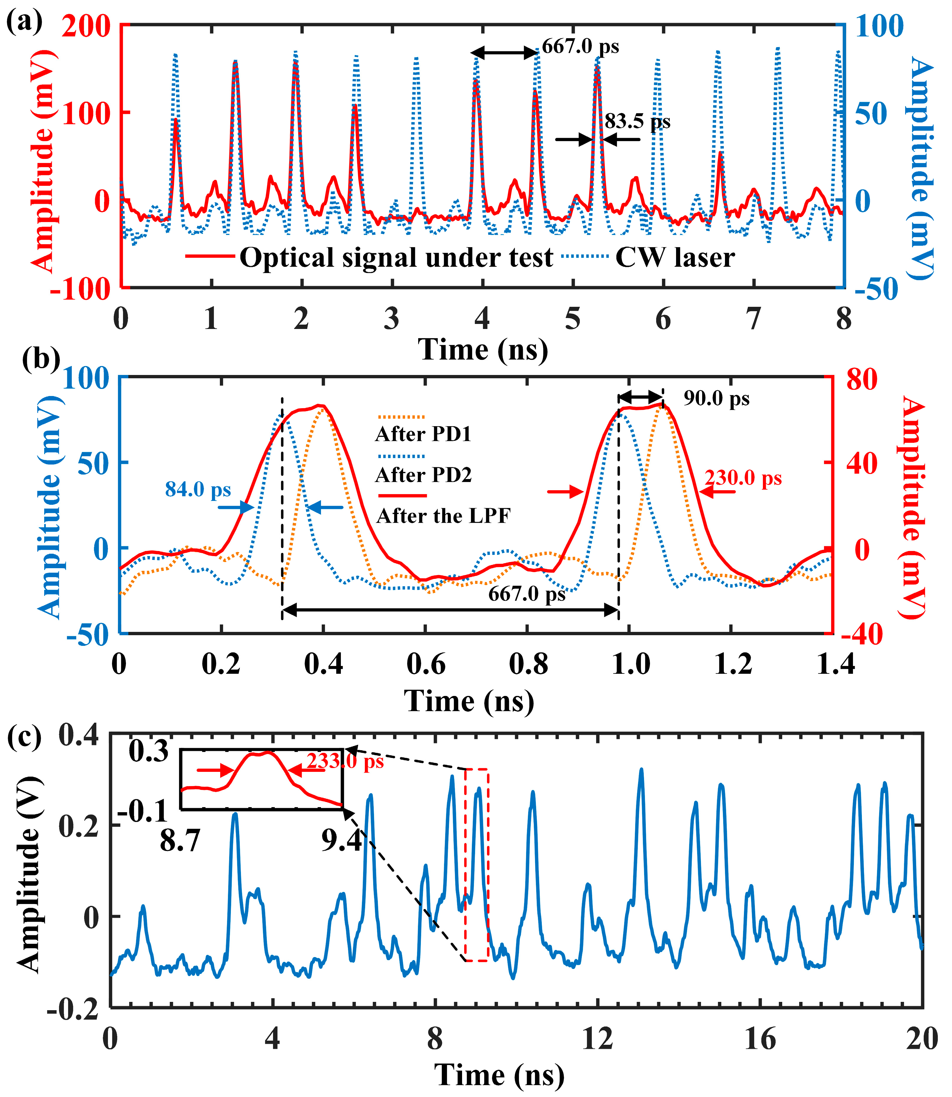
The gated on-off sampling performance is evaluated in
Figure 3a. The PPG was set to get an electrical pulse train with a frequency of 1.5 GHz and a pulse width of about 83.4 ps, and the electrical pulse train was used to modulate the optical signal injected into the MZM. The optical sampling pulse train plotted by the blue dashed line in
Figure 3a was measured using an oscilloscope (SDA 820Zi-B), when a continuous lightwave generated from an optical fiber laser (NKT photonics, Koheras BASIK E15) with an optical power of 0 dBm was injected into the MZM. It can be seen that an optical sampling pulse train with the same period of about 667.0 ps corresponds to a 1.5 GHz sample frequency, and the same pulse of about 83.5 ps as that of the electrical pulse. Replacing the optical fiber laser with a 2.5 G optical transmitter, the sampled optical pulse train after measuring the MZM is shown as the solid red line in
Figure 3a. The sampled pulse has the same pulse width of 83.5 ps as that of the electrical pulse.
The sampled optical pulse should then be quantized by the ADC with a maximum sampling rate of 2 Gsps. However, the pulse width of 83.5 ps cannot match the ADC sampling rate, resulting in a low quantization efficiency for the ADC used. To increase the quantization efficiency, the sampled optical pulse is broadened to match the ADC sampling rate. Here, an optical true-time delay technique is used to enlarge the pulse width.
Figure 3b shows the measured broadening process of the sampled optical pulse when the input lightwave is generated from an optical fiber laser. The sampled optical pulse is divided into two paths, transmitted through two optical fibers with a time delay difference of about 90 ps, and detected by two PDs. The outputs of the two PDs are plotted as the blue and yellow dashed lines in
Figure 3b, where the two pulse trains have a time delay of about 90 ps. The two pulse trains are then combined via an EC and filtered by an LPF with a 3 dB bandwidth of about 4 GHz. The filtered pulse is measured as the solid red line in
Figure 3b. It can be seen that the broadened pulse has a pulse width of about 230 ps, which matches the sampling rate of the ADC. Replacing the optical fiber laser with a 2.5 G optical transmitter, the sampled pulse train is plotted in
Figure 3c at a random 20 ns period. It can be seen that the sampled optical pulse is broadened, and the pulse width is about 233 ps, which matches the trace-and-hold capability of the ADC. In addition, the sampled pulse has a period of about 667 ps, corresponding to a sampling frequency of 1.5 GHz.
By then synchronizing the PPG and the ADC with a 1.5 GHz clock, the ADC sampling and quantizing time, or the ADC trace-and-hold window, is located at the flat top of the broadened sampled pulse. Consequently, the broadened sampled pulse is quantized by the ADC with high quantization efficiency. The sampling frequency is 1.5 GHz. In the demonstration, 524,288 points were recorded and used to obtain the eye diagram. Considering the 1.5 GHz sampling frequency, the recording time for the eye diagram is about 350 μs, corresponding to a 2.86 kHz update rate for the eye diagram recording.
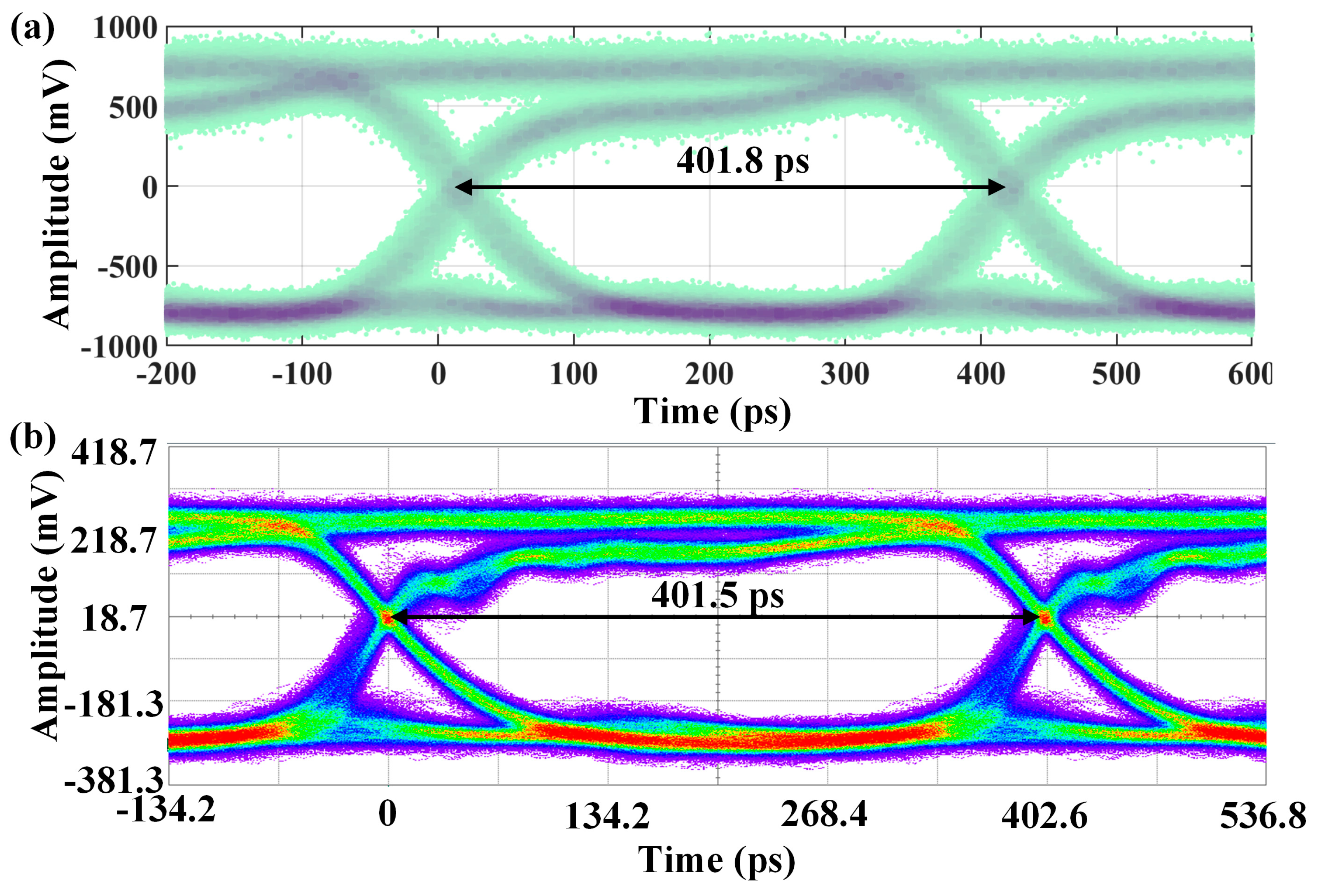
Figure 4a shows the eye diagram obtained from the quantized data recorded at 524,288 points. The eye width is measured to be about 401.8 ps, which agrees well with the measured 401.5 ps bit time in
Figure 2b. The eye diagram measured by the proposed time jitter method is also verified by the eye diagram measured by a commercial oscilloscope (SDA 820Zi-B), as shown in
Figure 4b, where the eye width at 401.5 ps is almost the same as that in
Figure 4a.
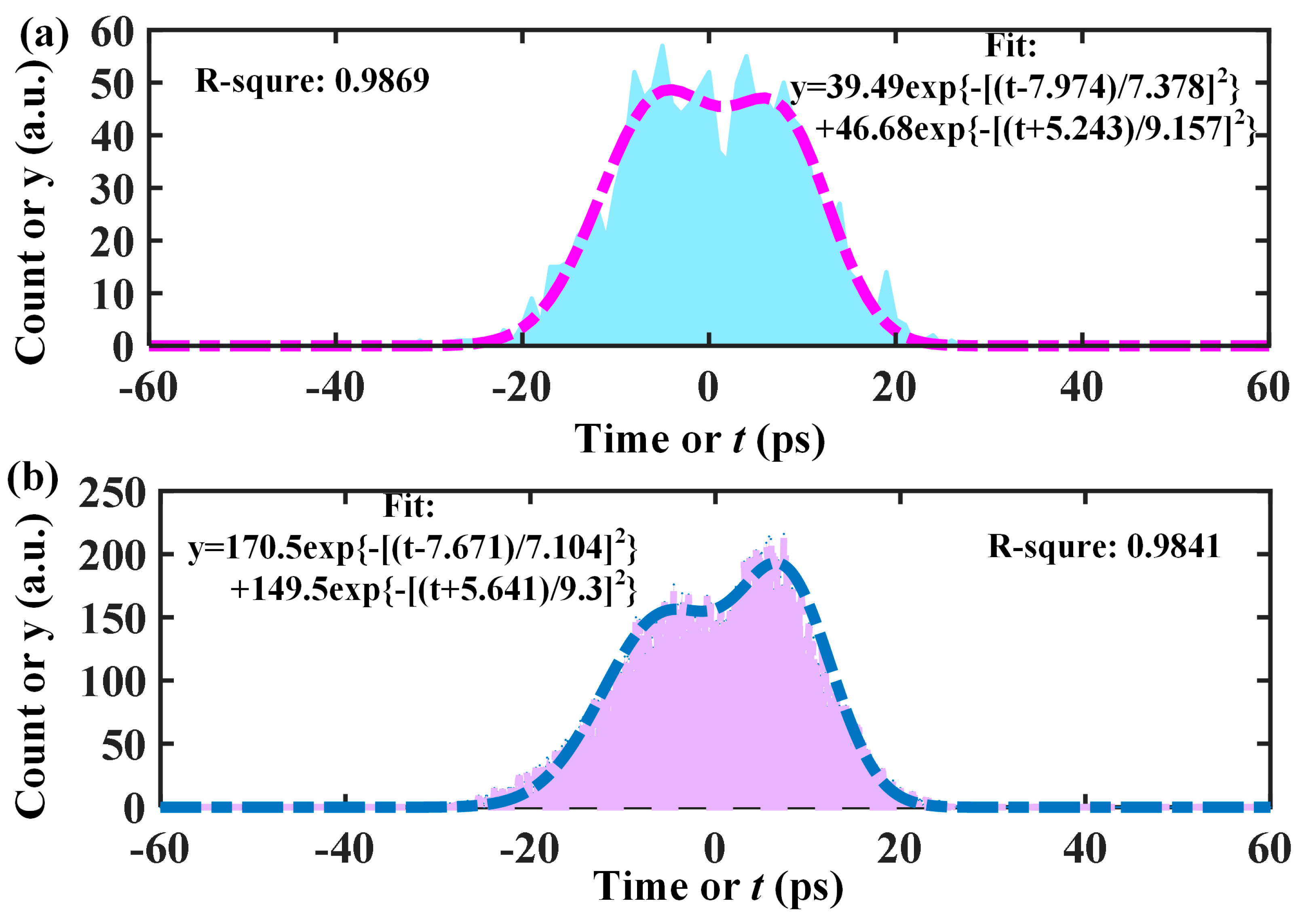
The time jitter histogram is then obtained in
Figure 5a based on the eye diagram data in
Figure 4a. It is shown that the histogram can be viewed as a dual-Dirac distribution. Thus, the jitter decomposition is implemented based on the dual-Dirac model described in Equations (1)–(5). The jitter histogram is fitted as y = 39.49 exp{−[(t−7.974)/7.378]
2} + 46.68 exp{−[(t + 5.243)/9.157]
2} with an R-square of 0.9869. The fitting result indicates that the jitter decomposition is implemented through dual-Dirac modeling. Specifically, the deterministic time positions are measured as 7.974 and −5.243 ps, corresponding to a DJ of about 13.20 ps. The standard deviations of the two Gaussian distributions at different deterministic time positions are 7.378/2
1/2 ≈ 5.2 and 9.157/2
1/2 ≈ 6.5 ps, corresponding to an RJ of (5.2 + 6.5)/2 = 5.85 ps. The measured TJ is then 13.2 + 5.85 = 19.05 ps. The jitter decomposition results are also verified by those measured by commercial oscilloscope (SDA 820Zi-B) in
Figure 5b, where the DJ, RJ, and TJ are measured to be 7.361 + 5.641 ≈ 13.00, (7.104/2
1/2 + 9.3/2
1/2)/2 ≈ 5.80, and 18.80 ps, respectively. It can be seen that the time jitter decomposition results achieved by the proposed jitter analysis method agree well with those of the commercial oscilloscope.


