Article

A High-Efficiency Single-Stage Isolated Sepic-Flyback AC–DC Led Driver

by
Kenan Gürçam
1,* and
Mehmet Nuri Almalı
2
1
Department of Electrical and Electronics Engineering, Igdir University, Igdir 76000, Türkiye
2
Department of Electrical and Electronics Engineering, Van Yuzuncu Yil University, Van 65090, Türkiye
*
Author to whom correspondence should be addressed.
Electronics 2023, 12(24), 4946; https://doi.org/10.3390/electronics12244946
Submission received: 9 November 2023 / Revised: 6 December 2023 / Accepted: 7 December 2023 / Published: 9 December 2023

Abstract

:
Regulating LED current and voltage is critical to maintaining a constant luminous flux in AC- or DC-powered LED lighting circuits. Today, users require constant current drivers that can provide a wide range of output voltages to drive different numbers of series-connected LED arrays. This work proposes an LED driver by combining an isolated SEPIC converter operating in the continuous conduction mode (CCM) and a modified Vienna rectifier. The proposed LED driver offers a single-switch control structure by adding a Vienna rectifier to the integrated SEPIC-FLYBACK converter. This driver structure provides many advantages over traditional bridge rectifier structures. The prototype circuit was tested in an 18 W continuous current mode (CCM) to verify its feasibility. As a result of the values obtained from both simulation and prototype circuit models, it has been shown to provide many of the following advantages: 95% high efficiency, high reliability, 4% low total harmonic distortion, 97% high power factor, and 70 V low switching voltage. This work meets class C 3-2 and IEC 61000 standards.

1. Introduction

With the rapid advancement of technology, energy consumption is increasing, and energy-saving plans are the main agenda of the countries [1]. Since a significant part of the energy consumption in the world is used for lighting, countries are creating energy-saving plans in this direction [2,3]. LEDs have started to be used instead of traditional lighting devices with many advantages such as long life, low energy consumption, and developing technology. Studies on rectifier circuits to develop new LED driver topologies have attracted the attention of researchers [4]. Since LED driver circuits use high-frequency switching elements, it causes harmonic distortion in the input current. The high-distortion current on the input side of the LED driver circuits also negatively affects the overall compatibility of the network. For this reason, a two-part structure between the output side and the input side of the circuit has been proposed in many LED topologies. In the first stage, a DC–DC converter is used to operate under different load conditions on the output side, while a PFC circuit is used in the second stage to prevent the current drawn from causing harmonic distortion on the input side. Due to these two-stage structures in the driver circuits, more power switches are needed. This causes the control of the circuit to become more complex [5,6]. Topologies that control the DC–DC converter and PFC circuit with a single switch are widely used to minimize the number of switches. Thus, the control of the circuit is simplified, and its size and cost are reduced [7,8].
Due to their simple structures and ease of control, Boost, Buck–Boost, SEPIC, and CUK converters are mostly used in LED drivers. These converters are preferred in LED applications because the PFC structure is easy and highly efficient. However, since the output voltage is lower than the peak value of the input, it causes high voltage in the power switches [9]. To address this shortcoming, many converters have been designed using the soft switching methods of power switches. One of these converters is the SEPIC converter, which reduces the voltage stress on the switches with the effect of the storage capacitor in its structure [10,11]. However, SEPIC converters have more components, resulting in higher costs and lower efficiency. Another converter is the Buck–Boost converter, which is the most widely used converter due to its many advantages such as simple circuit structure and high power factor [12,13].
LLC, Class E, FLYBACK, and FORWARD converters are used in applications where constant output current and electrical isolation are required in LED drivers [14,15]. In particular, LLC converters have high efficiency due to their soft switching feature, but the high number of elements in the circuit causes control complexities and high costs [16]. Although Class E resonant converters have high conversion efficiency due to their soft switching feature, they are not preferred due to the large number of components in the circuit structure and control difficulties. FLYBACK and FORWARD converters are widely used in low-power applications due to their simple circuit structures, ease of control, and low cost [17]. However, it causes voltage increases on the switches due to the leakage inductance of the transformer in the circuit. Also, the energy stored in the inductor when the switch is in the open state limits the use of the magnetic core [18].
Lee et al. designed a new converter by adding a lossless suppression circuit to the Boost–FLYBACK converter. With their proposed converter, DC-BUS capacitor voltage is reduced, and recycling efficiency is increased [19]. Yadav et al. proposed a new converter that provides a high output efficiency by combining Viana, CUK, and FLYBACK converters with a single switch [20]. In another study, they designed a new converter with a low THD value by combining SEPIC and FLYBACK converters with a single switch [21]. A new driver with a high PFC value was designed by combining a Buck–Boost converter and a reverse-coupled inductor with a single switch by Cheng et al. [22]. Regulating the LED current is critical to maintaining a constant luminous flux in LED lighting circuits powered by AC or DC sources. Effective LED drivers improve power quality and efficiency while keeping low THD values, which is very important.
In this study, a single-stage-isolated SEPIC–FLYBACK AC–DC LED driver circuit is designed. The proposed LED driver circuit consists of two main parts. The first part is the AC-DC converter structure consisting of a single-phase modified Vienna converter. The second part is the SEPIC–FLYBACK converter combination, which provides an isolated voltage structure. The article is organized as follows: The main circuit of the proposed LED driver is introduced in Section 2. In Section 3, the operating modes of the proposed circuit are presented in detail. The model design is given in Section 4 with its mathematical calculations. In Section 5, simulation and experimental studies of the proposed circuit are given. Finally, the conclusions are presented in Section 6.

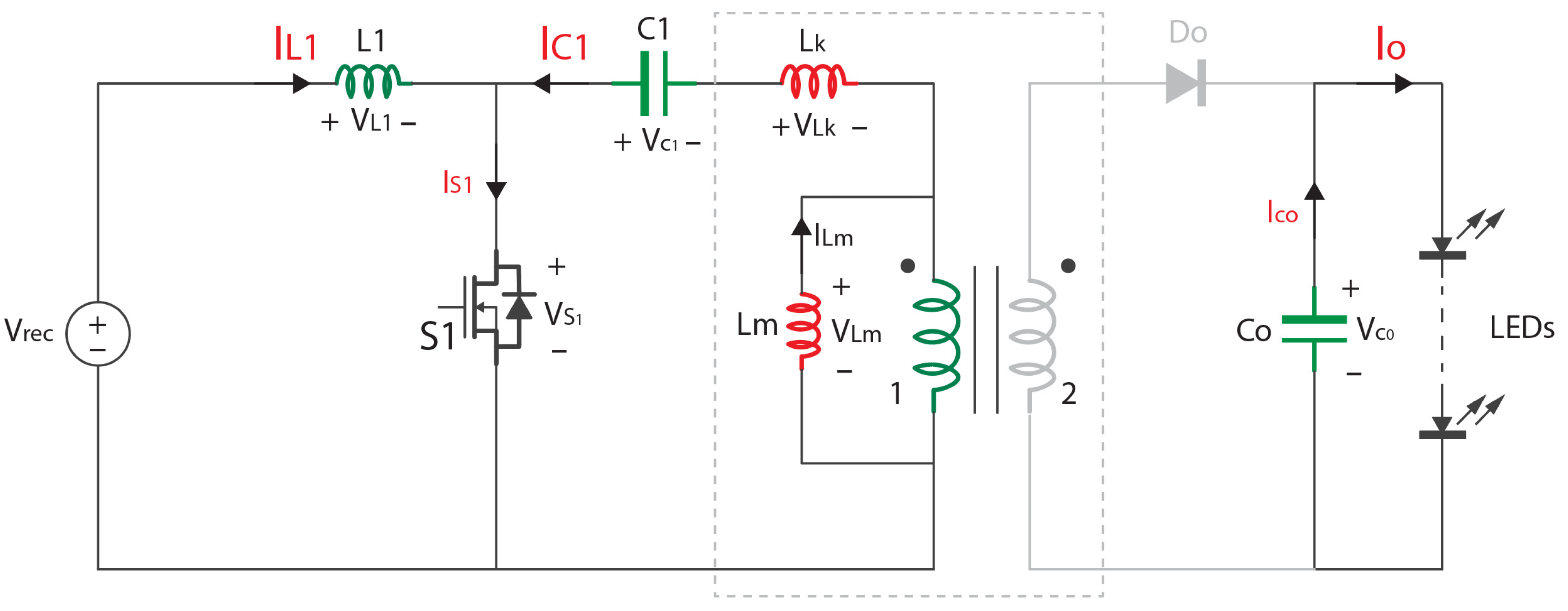
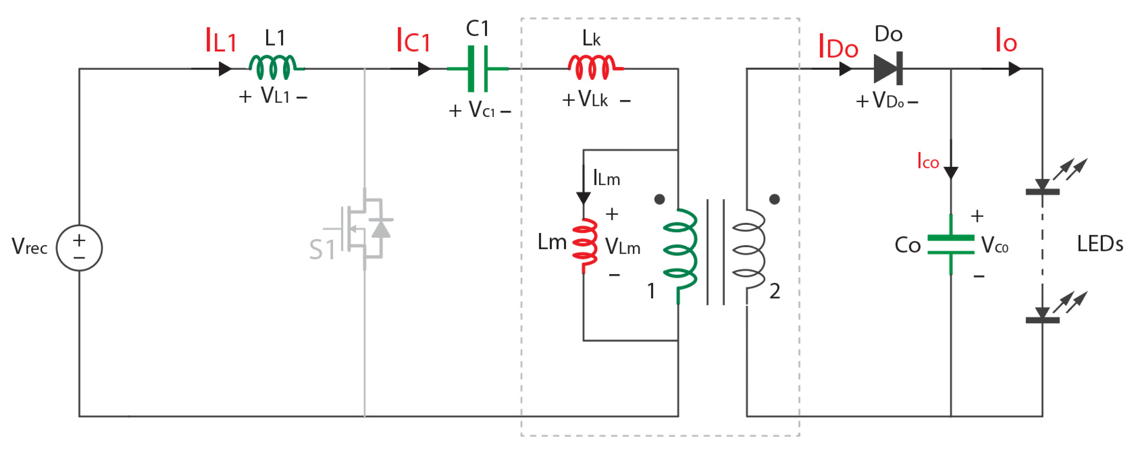
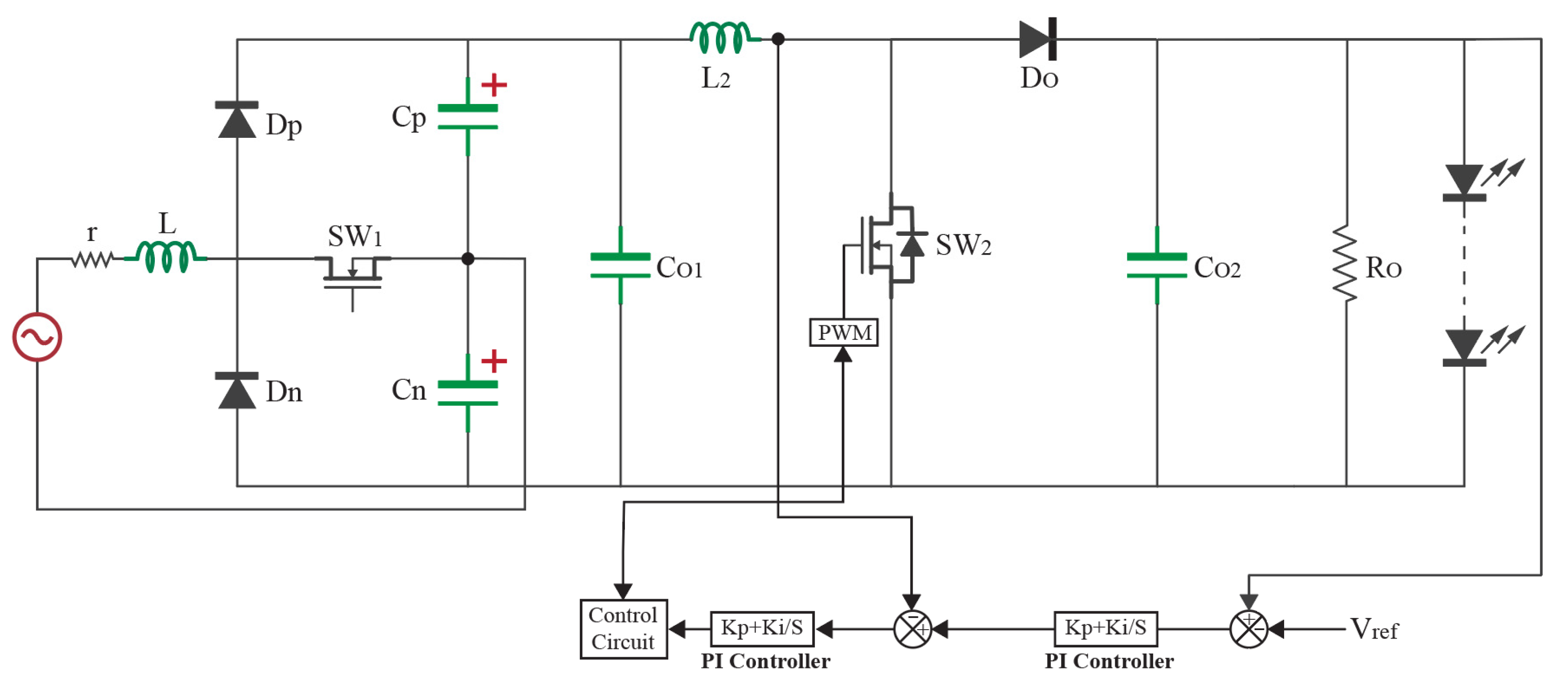
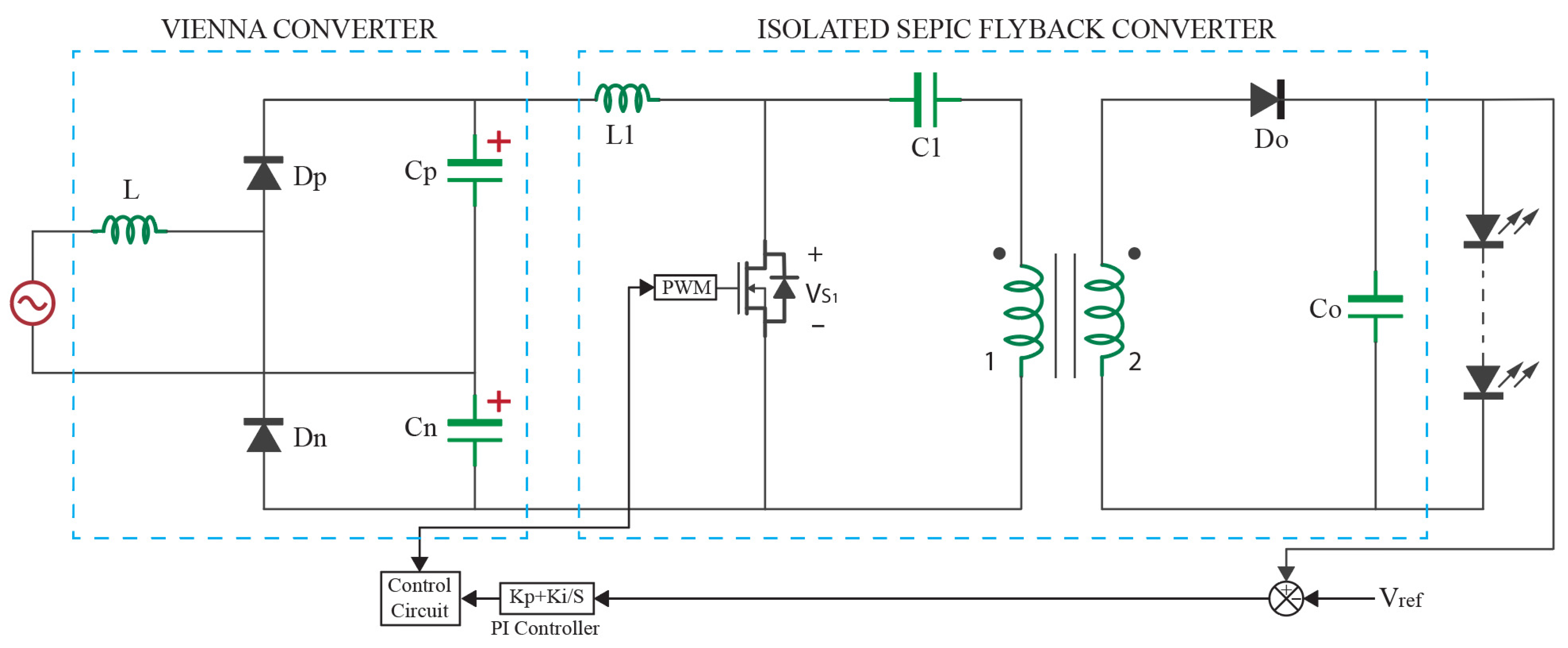
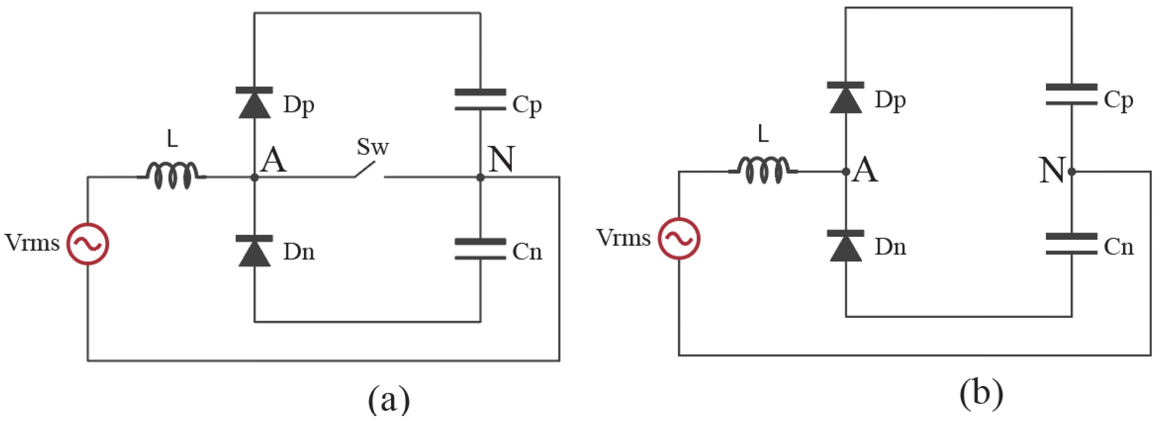
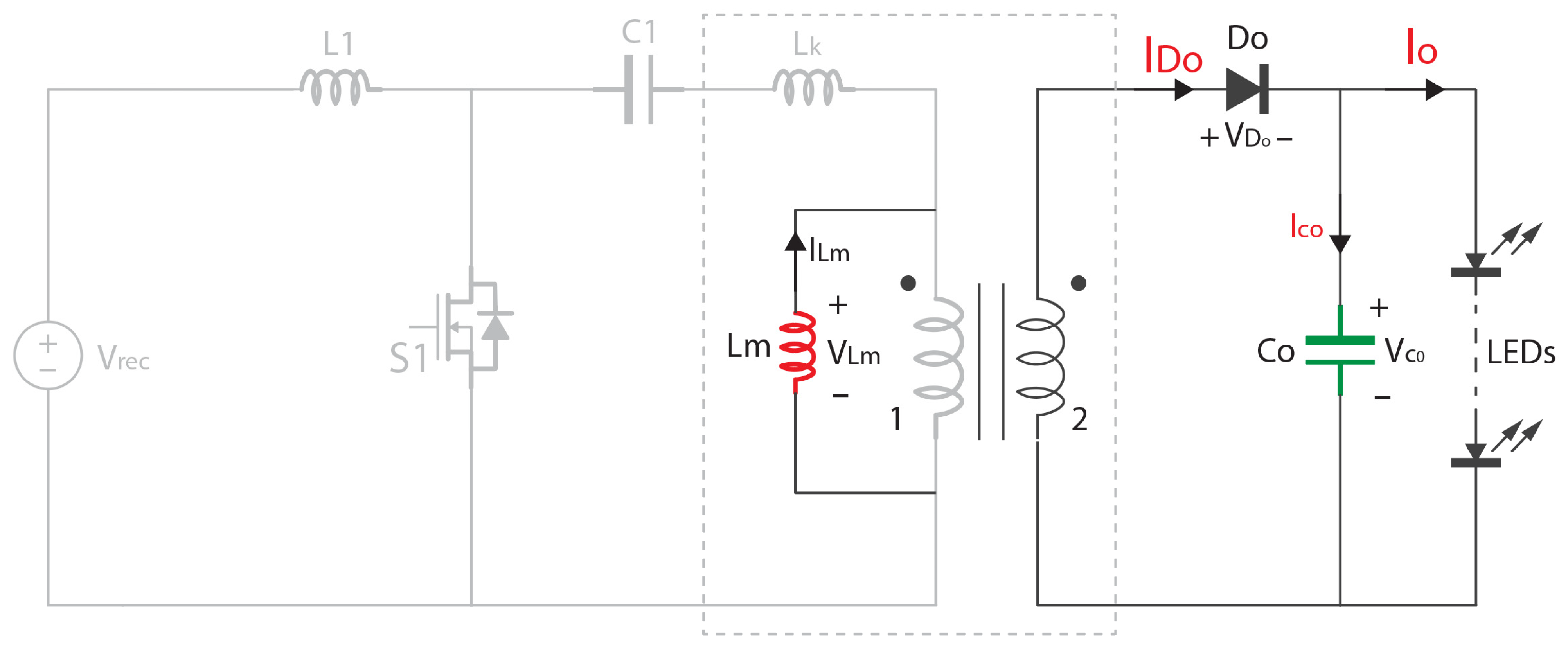
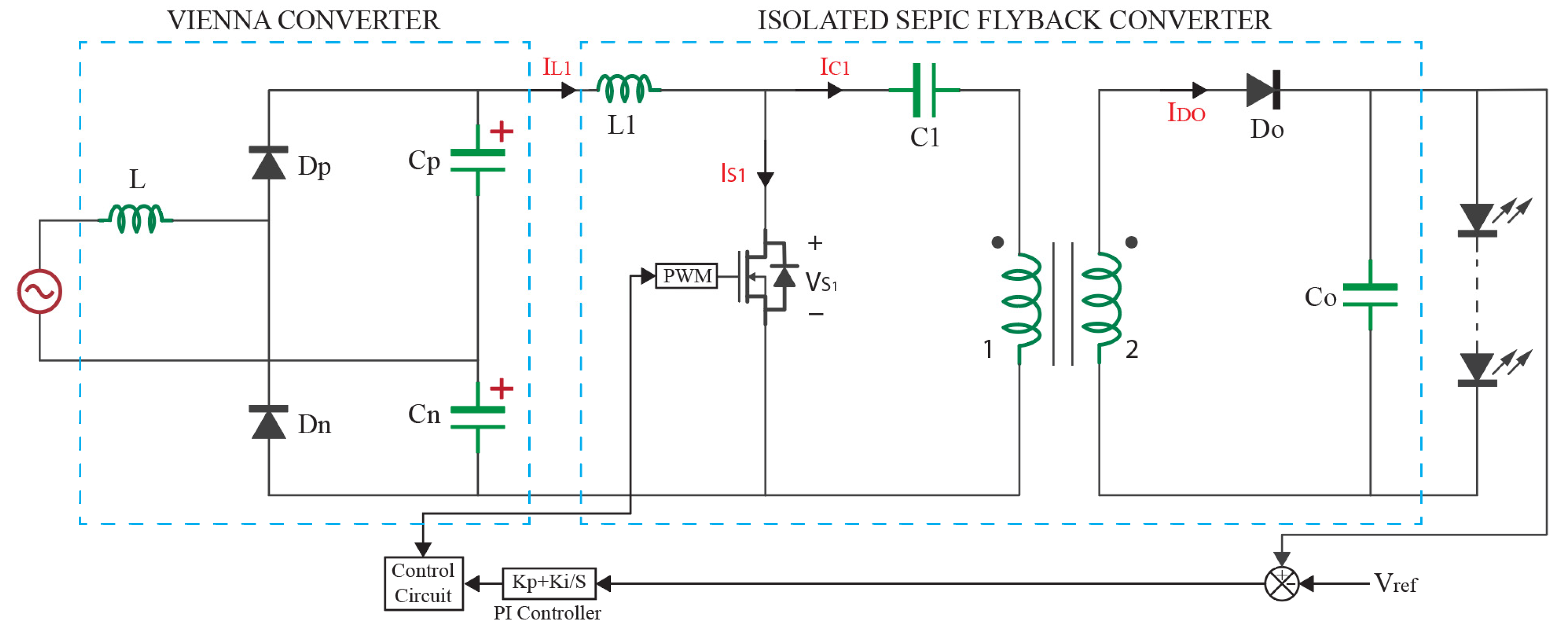
2. Proposed Led Driver Circuit

Figure 1 shows the topology of a two-stage Vienna rectifier and a high-power factor LED driver.
When the circuit given in Figure 1 is examined, it is seen that the switch stress is reduced with a modified Vienna rectifier, but the control of the circuit becomes complicated due to the non-isolated structure of the circuit and the use of two switches.
In this study, a new single-stage LED driver circuit is proposed by arranging a two-stage Vienna rectifier circuit and adding an isolated SEPIC converter with an output that is combined with a single switch. A simplified switched circuit topology of the proposed circuit is given in Figure 2.
When the structure of the circuit is examined, the DC output voltage is kept at the appropriate level by choosing the desired value of the DC output voltage, Cp, and Cn capacitor values by using a filtering inductance L to the AC input and a modified Vienna rectifier. L1 and C1 elements perform both the energy storage function and the power factor correction (PFC) function. Circuit isolation is provided by the isolation transformer used in the circuit. The Co output capacitor minimizes the fluctuations in the output voltage and also extends the life of the circuit since it is a non-electrolyte capacitor.

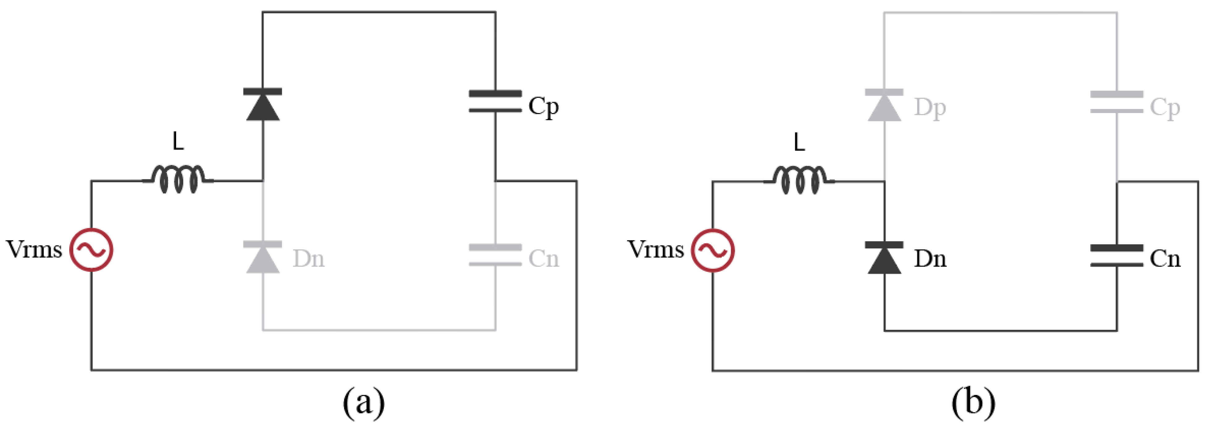
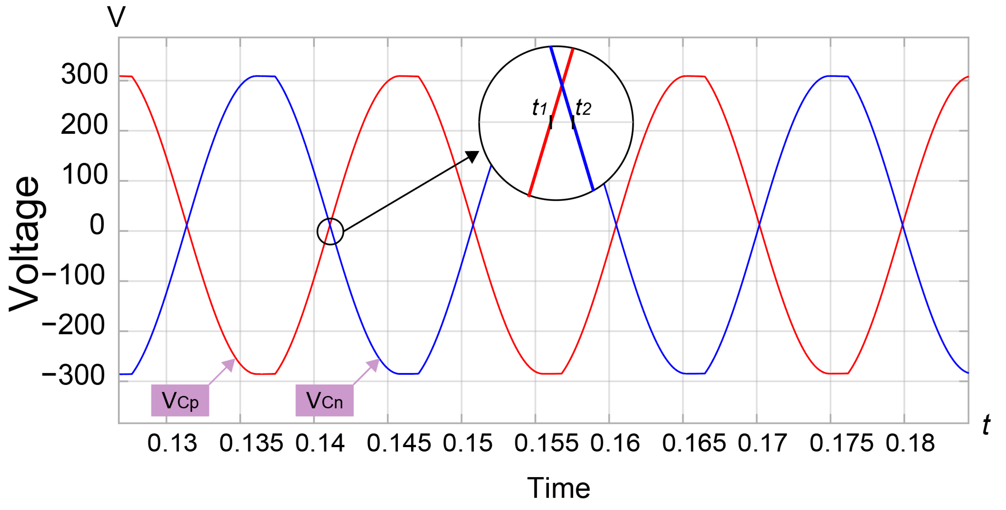
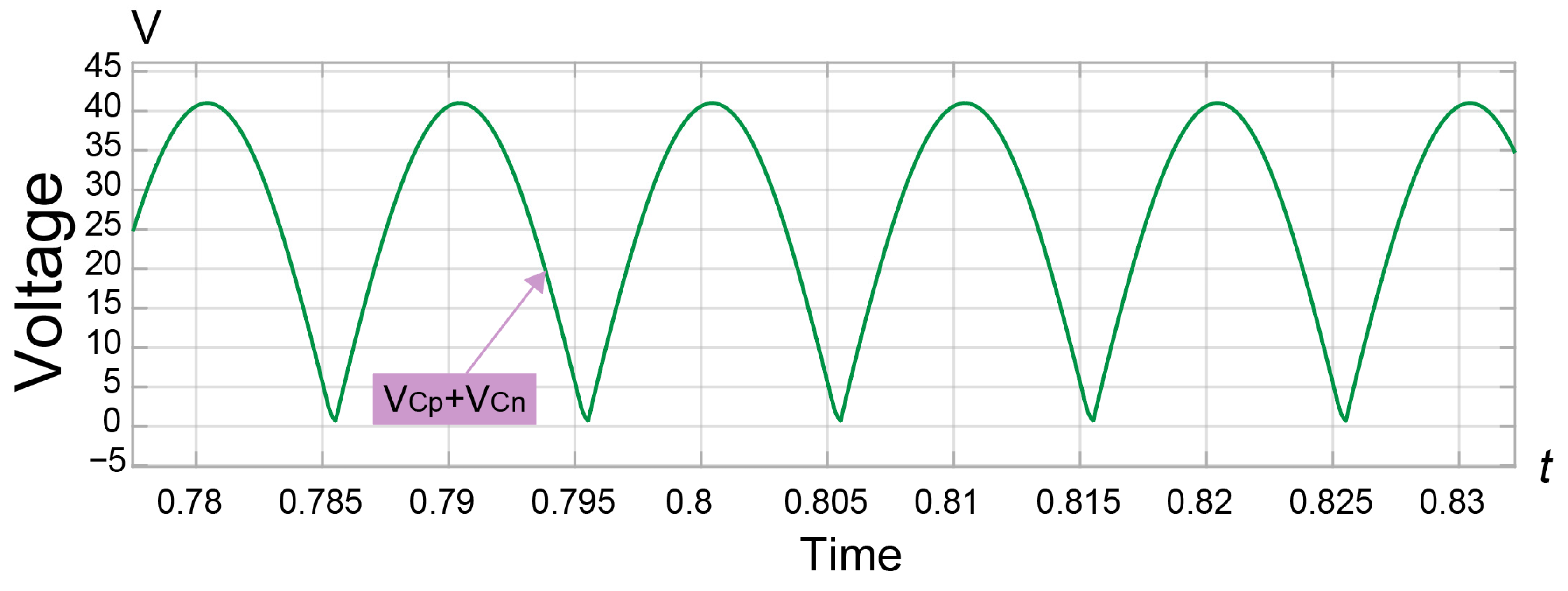
Vienna Rectifier Analysis and Design

A single-phase conventional Vienna rectifier is shown in Figure 3a. The Sw switch in the classical Vienna rectifier was removed, and the Vienna rectifier shown in Figure 3b was used. Here, Dp and Dn diodes are source side diodes operating for one phase of AC sinusoidal source. L represents the source filter inductor and the capacitors Cp, and Cn represents the rectifier output [23].
The modified Vienna rectifier operating modes are presented in Figure 4a,b.
As seen in Figure 4, the main circuit consists of two diodes, two series capacitors, and an inductor. Diode connections allow capacitors to be charged at equal voltage and opposite polarity. The capacitor voltages in the circuit are given in Figure 5.
Depending on the state of switch Sw, the single-phase Vienna rectifier circuit (Figure 3a) is characterized by three voltage states between the anode point of diode Dp and the common point of the two capacitors Cp and Cn. There are various control algorithms for switch S proposed to achieve specific characteristics such as harmonic composition, THD, etc. However, the proposed modified Vienna rectifier produces DC voltage without the need for any switch by using the difference voltages in the Cp and Cn capacitors. Figure 5 shows the output voltage of capacitors Cp and Cn. As seen in the figure, since the capacitor voltages are of the same polarity in the t1-t2 interval, the total voltage will not be zero. Therefore, the sum of the capacitor voltages will be greater than zero at all intervals. Hence, DC output voltage is provided without the need for any switch.
The total output voltage is taken from the ends of the capacitors connected in series, and the voltage waveform is shown in Figure 6.

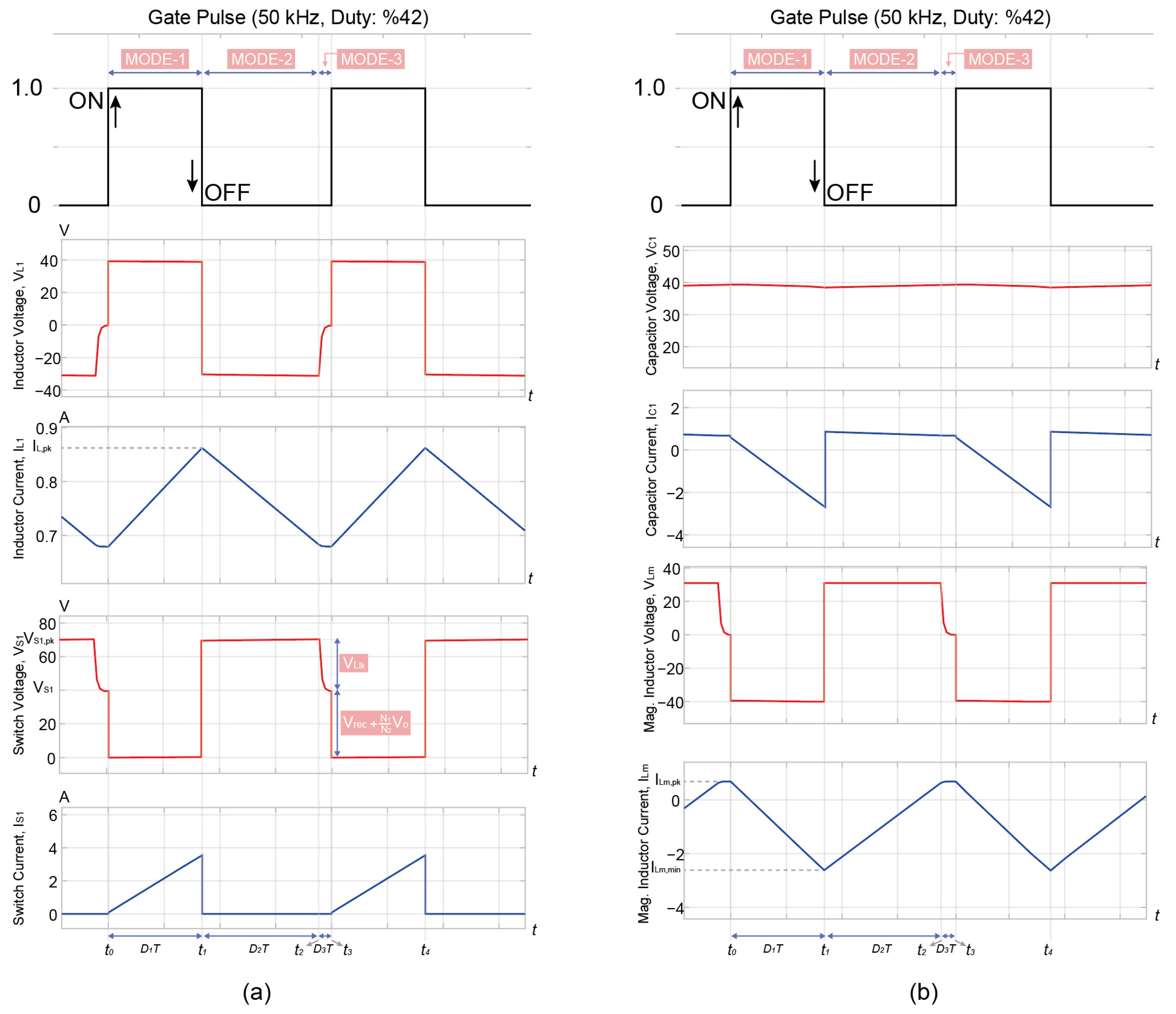
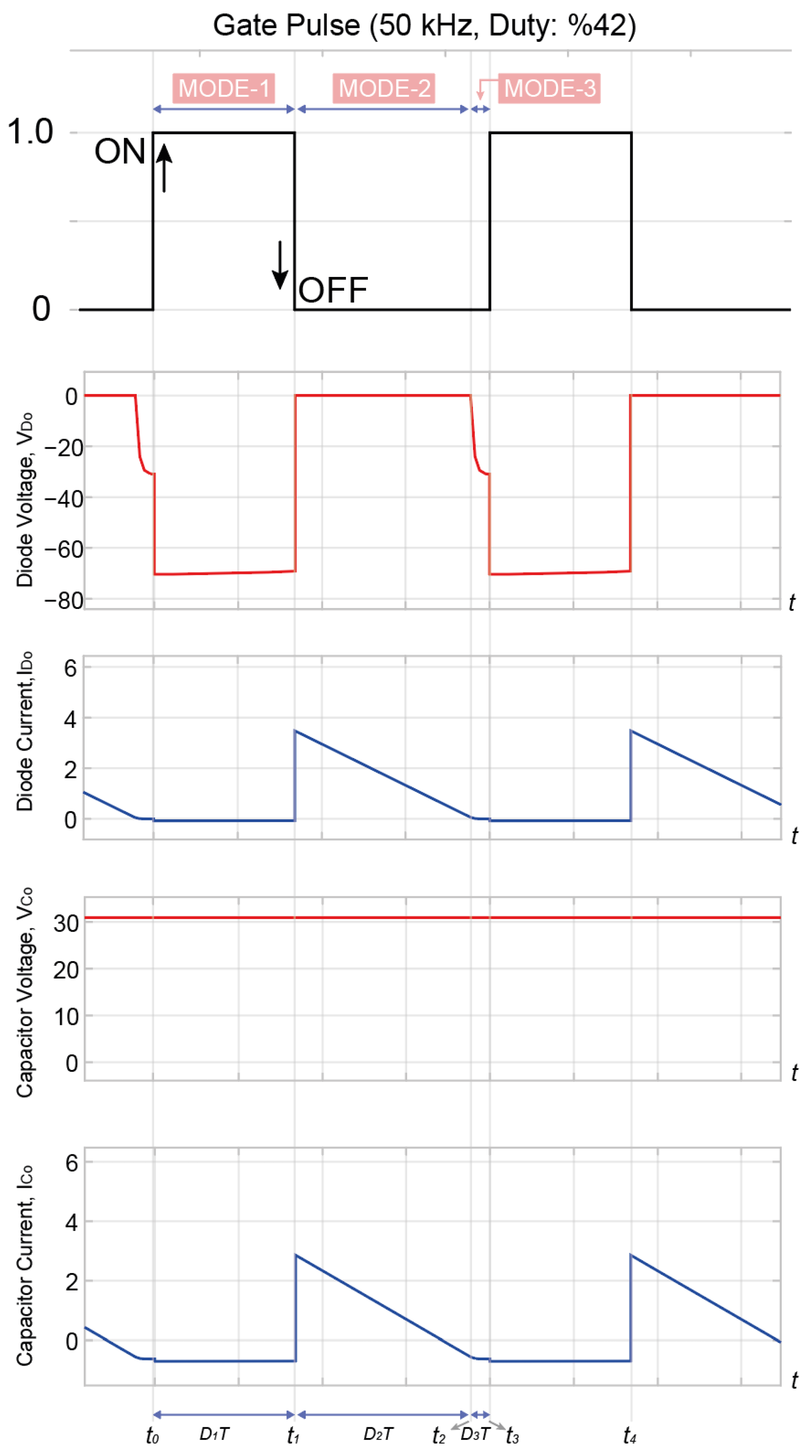
3. Operating Modes of The Recommended Circuit

The LED driver suggested in Figure 2 works in three main modes. These operating modes are described below, respectively.

3.1. Mod I [t0 ≤ t < t1]

The first mode of operation of the designed circuit, Mode I, is given in Figure 7.
As seen in Figure 7, the Mode I operation starts with the closing of switch S1. The current from the DC source is stored on the inductor L1, and the energy in the capacitor C1 is discharged through the magnetizing inductor Lm and the leakage inductance Lk. The current through switch S1 is equal to the sum of the capacitor current IC1 and the inductor current L1. The current flowing through the switch S1 is calculated by Equation (1).
I S 1 ( t ) = I L 1 ( t ) + I C 1 ( t )
In Mode I, there is no current flow because the Do output diode is reverse-biased. Therefore, the LED load is energized through the Co output capacitor.

3.2. Mod II [t1 ≤ t < t2]

The second operating mode of the designed circuit, Mode II, is given in Figure 8.
As seen in Figure 8, Mode II operating mode starts when the S1 switch is opened at t = t1 instant. The energy in the L1 inductor begins to be transferred to the load through C1. With the magnetizing inductor Lm, the current through the leakage inductance Lk resists the sudden change. Thus, sudden voltage spikes are limited. In this mode, since the polarities of the transformer are changed, the diode Do is forward biased, and the voltage in the primary winding of the transformer is transferred to the secondary winding. Subsequently, both the Co capacitor is charged and the LED feeds the load.
In a steady state, assuming the transformer leakage inductance is small enough to be neglected, the switch voltage S1 is expressed as VS1, and Equation (2) is calculated by the given equation.
V S 1 = V r e c + N 1 N 2 V o
If N1/N2 = 1 is taken in Figure 7, the L1 current is continuous since the IL1 current does not fall to zero. The direct current from the Vienna rectifier is transmitted to the primary winding of the transformer through the inductor L1 and the capacitor C1. The magnetizing inductance Lm resists the sudden polarity change as it is the polar opposite at the first moment; then, it stores energy in the same polarity until the end of the operating mode.

3.3. Mod III [t2 ≤ t < t3]

The Mode III operating mode of the designed circuit is given in Figure 9.
As seen in Figure 9, capacitor C1 terminates the current flowing through it when it reaches full charge. The energy stored on the magnetizing inductor Lm is transferred to the transformer’s primary windings. In this case, since the polarity at the transformer winding ends will change, the Do output diode is forced to cut. When the Do diode is turned off, the load is fed through the Co capacitor again.
In Figure 2, the L1 input inductor voltage–current plot and S1 Switch voltage–current plot in all operating modes of the proposed LED driver are given in Figure 10a, C1 Storage capacitor voltage–current plot and Lm magnetization inductor voltage-current plot are given in Figure 10b. In the graph given in Figure 10, the operating modes of the circuit show the behavior of the switch during the ON–OFF time. The time-dependent behavior of the circuit elements is presented in detail.
The output diode Do voltage-current graph and output capacitor Co voltage–current graph in the proposed LED driver are given in Figure 11. Circuit operating in continuous conduction mode (CCM) operates in multiple modes within one switching period. As can be seen from the operating modes, the switch voltage does not increase while providing a constant output current at the reference load. In this way, excessive voltage spikes on the switch are limited.

4. Design of the Recommended Led Drive

4.1. Calculation of Input Inductor L1

The circuit proposed in Figure 2 is designed to provide constant output current at variable loads, and the most ideal circuit elements have been optimized and selected. The circuit is operated at a constant reference load at the switching frequency and duty cycle of switch S1. In the first approach, the transformer used in the isolated SEPIC converter is assumed to be ideal. Since the IL1 current does not drop to zero, the LED driver is designed to operate in continuous conduction mode. If the input power of the circuit (Pin) is assumed to be equal to the output power (Po), it is calculated by the equation given in (3).
P i n = P o V r e c . I L 1 = ( V 0 ) 2 R
Vrec represents the output voltage of the modified Vienna rectifier, and the average current value of the inductor L1 is expressed as IL1. The output voltage of the LED driver is represented as Vo, and R is considered as the equivalent static resistance of the modeled LEDs. The average output voltage of the Vienna rectifier is calculated by the equation given in Equation (4).
V r e c = V m 2 π
The maximum value of the AC input voltage is represented as Vm, and the average value of the input inductor current IL1 is calculated by the equation given in Equation (5).
I L 1 = 1 T [ t 0 t 1 I L 1 , max . t D 1 . T d t + t 2 t 3 ( I L 1 , max . t D 2 . T + I L 1 , p k ) . d t ] = 1 T [ I L 1 , max D 1 . T t 2 2 | t 0 t 1 + I L 1 , max D 2 . T t 2 2 | t 2 t 3 + I L 1 . t | t 2 t 3 ] , = I L 1 , p k T [ ( D 1 . T ) 2 D 1 T 2 ( D 2 . T ) 2 2 D 2 T + D 2 T ] , I L 1 = Δ I L 1 2 ( D 1 + D 2 ) ,
D1, D2, and D3 are Mode I, II, and III times. (Mode III time is negligible.) T is the time in the transition interval. The change in input inductor current as ΔIL1 is calculated by Equation (6).
Δ i L 1 = ( N 1 N 2 ) V 0 D 2 T L 1
IL1 inductor average current from Equation (6) is calculated with the equation given (7) when it is substituted in Equation (5).
Δ i L 1 = ( N 1 N 2 ) V 0 D 2 T ( D 1 + D 2 ) 2 L 1
Using the input and output power equation, the input inductor L1 value is calculated with the equation given in Equation (8).
( 2 V m π ) . ( N 1 N 2 ) V 0 D 2 T ( D 1 + D 2 ) 2 L 1 = V o R 2 L 1 = V m . D 2 . T . R . ( D 1 + D 2 ) ( N 2 N 1 ) . V 0 . π
During boundary transmission mode, D1 = (1 − D2) is calculated with the given equation.

4.2. Calculation of Magnetization Inductor Lm

The output current ripple ΔIo is proportional to the current ripple present in the magnetizing inductor of the transformer. Therefore, the transformer is designed to operate in continuous mode and low magnetizing inductor current ripple to provide a smaller output current ripple and a smaller output capacitor. When the switch S1 is closed, the magnetizing inductor current is calculated by Equation (9).
I L m = I C 1 N 2 N 1 I D 0
On the secondary side, diode current IDo is calculated by the equation given in Equation (10).
I D 0 = I C o + I 0
In a steady state, the average currents of capacitors C1 and Co are zero. Therefore, the average value of the magnetizing inductor current is calculated by the equation given in Equation (11).
I L m = i C 1 N 2 N 1 ( i C o + I o )
I L m = | N 2 N 1 I o |
The operation of the circuit in continuous conduction mode works in the CCM when the minimum magnetizing inductor current ILm min > 0.
Δ I L m 2 I L m = 0
When switch S1 is ON state
V C 1 + V L m = 0
Since the average voltage of the capacitor C1 is equal to Vrec, the magnetizing inductor current (15) is calculated by the given equation
V L m = V m 2 π
The time-dependent current change ∆ILm over the magnetization inductor is calculated by Equation (16).
Δ i L m = V m D 1 T 2 π L m
If Equations (12) and (16) are substituted in Equation (17).
V m D 1 T π L m N 2 N 1 I o = 0
In order for the circuit to work in the CCM, the magnetizing inductance value must be selected greater than the inductor value calculated in (17). The magnetizing inductance Lm value is calculated by the equation given in Equation (18).
L m > V m D 1 T N 1 π N 2 I o

4.3. Calculation of Storage Capacitor C1

When the switch S1 is opened, the change in the charge of C1 is calculated by the equation given in Equation (19).
| Δ θ C 1 | = 1 2 ( i L m , min + i L m , max ) D 1 T
The values of the minimum current value ILm,min and maximum current value ILm,max of the magnetizing inductor are calculated by the equation given in Equations (20) and (21).
i L m , min = N 2 N 1 I o + V m D 1 T π L m
i L m , max = N 2 N 1 I o V m D 1 T π L m
Equations (18) and (19) are written in (17), and the C1 capacitor value is calculated with the equation given in Equation (22).
Δ θ C 1 = N 2 N 1 I o D 1 T
The charge change value on the storage capacitor C1 is calculated by the given Equation (23).
C 1 = Δ θ C 1 Δ V C 1
If Equation (22) is written instead of (23), the value of C1 is calculated with the equation given in Equation (24).
C 1 = I o D 1 T N 2 Δ V C 1 N 1
The average output current Io = Vo/R. Therefore, the C1 storage capacitor is calculated by the given Equation (25).
C 1 = D 1 T N 2 R N 1 ( Δ V C 1 V o )
When switch S1 is opened,
V r e c = V L 1 + V C 1 + ( V I k + V L m )
Since the average voltage across the inductors is zero, the average voltage of the storage capacitor C1 is calculated by the given Equation (27).
V C 1 = V m 2 π
The change in average voltage across C1 is calculated by Equation (28) given.
V C 1 , r i p = Δ V C 1 V C 1
If we substitute Equations (27) and (28) in Equation (25), the value of the C1 capacitor is calculated with the equation given in Equation (29).
C 1 = D 1 T N 2 R N 1 ( V m V C 1 , r i p 2 π V o )

4.4. Output Capacitor Co Calculation

When the switch S1 is opened, the voltage on the output capacitor Co and the output voltage Vo are equal to each other. Equation (30) expressing the charge change on the Co capacitor is calculated with the given equation.
| Δ θ C 1 | = C o Δ V C o = V o R D 1 T
T is twice the line period of 10 ms. If the equation numbered (30) of the Co output capacitor is rearranged, Equation (31) is calculated with the given equation.
C o = V o D 1 T Δ V o R

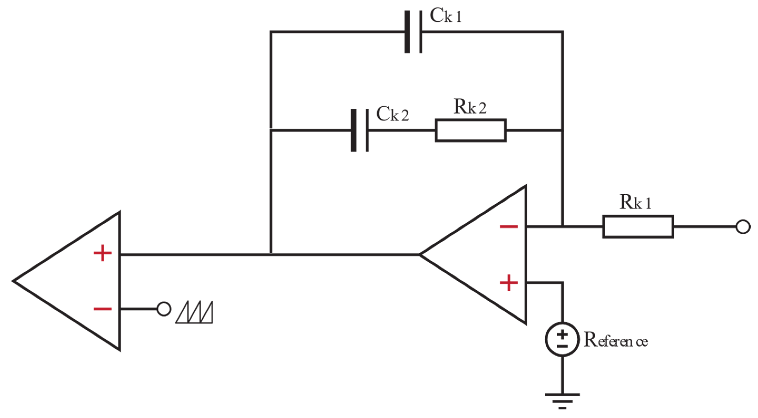
4.5. Control Loop Design

In the control loop design, the LED current is under constant surveillance using a series-connected resistor (Rs) within the LED array circuit. The measured current is then juxtaposed with a predetermined reference value. The control system used a simple proportional–integral (PI) controller, as shown in Figure 12.
The PI controller processes the error signal obtained from the comparison between the detected LED current and the reference value. The controller’s output is then compared to the fixed-frequency sawtooth waveform. In response to changes in output current, the controller dynamically regulates the duty cycle of the system. This adaptation ensures a constant output current even in the presence of variable loads. Dynamic regulation keeps the LED current at a consistent level across the entire operating voltage spectrum.

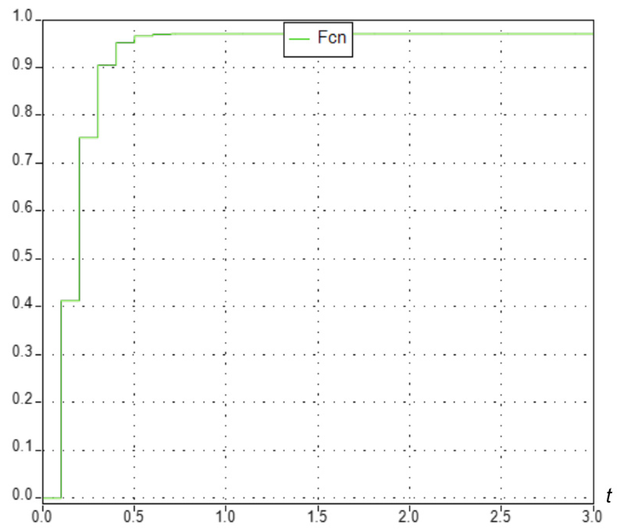
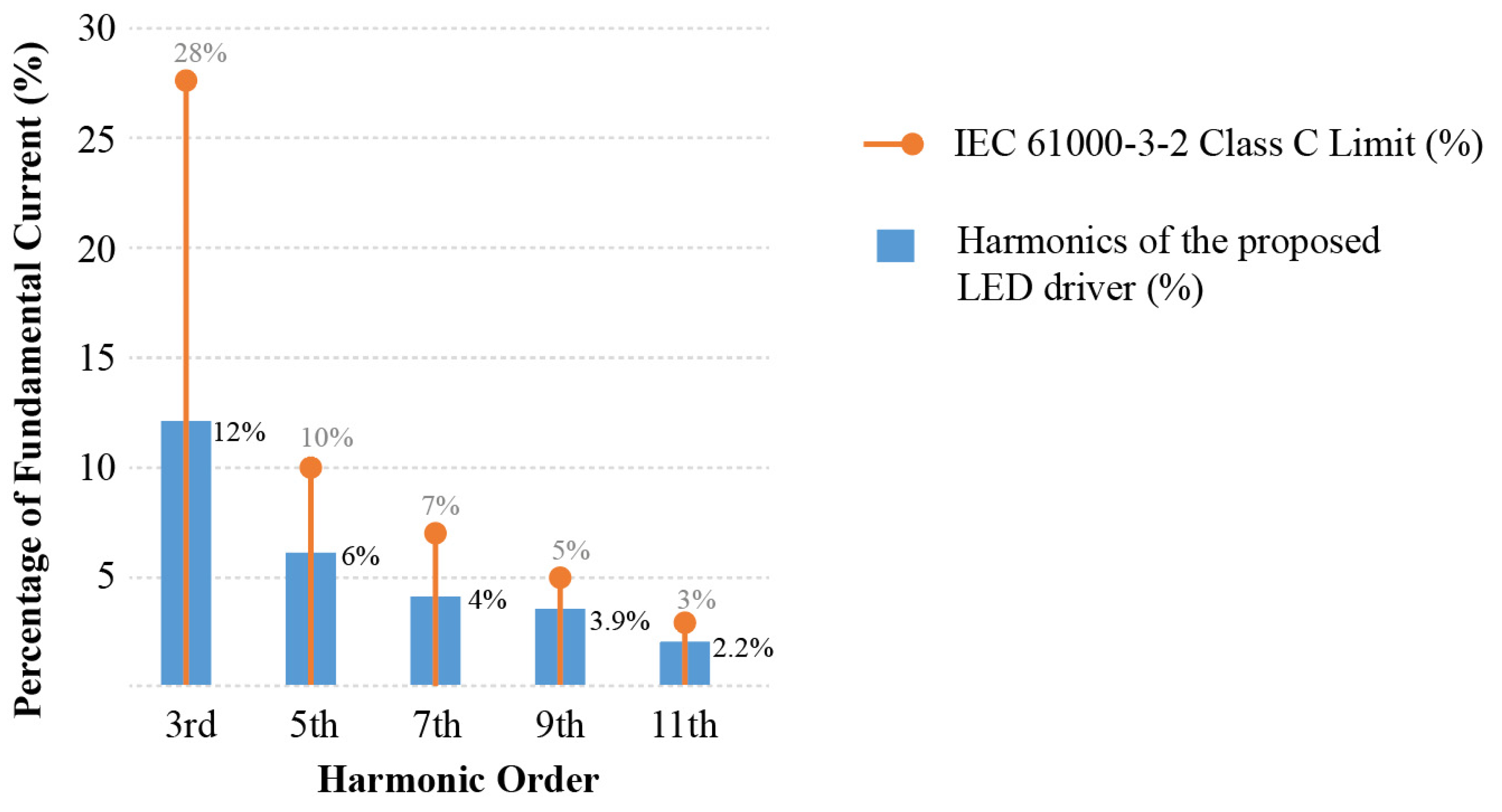
5. Result and Discussion

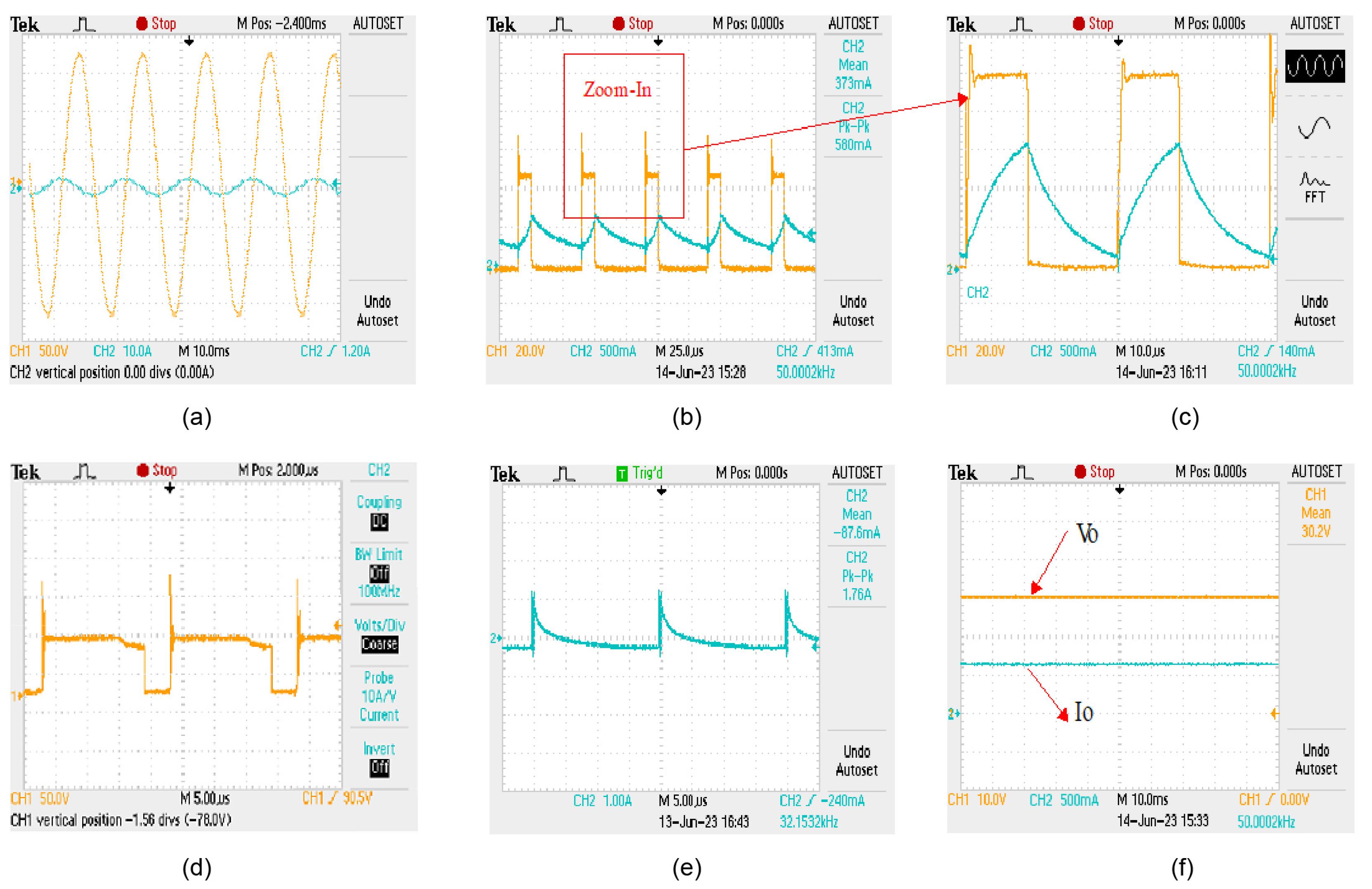
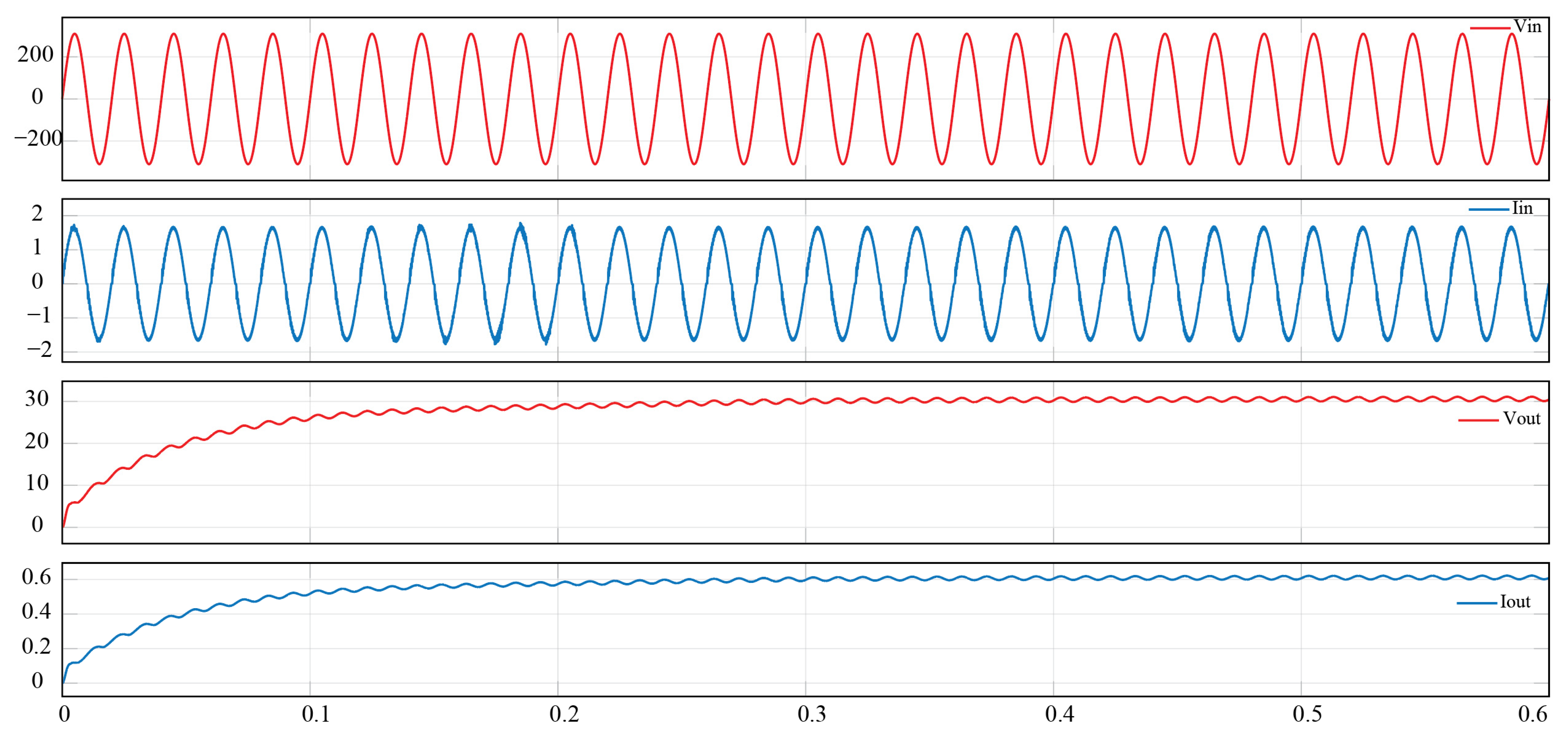
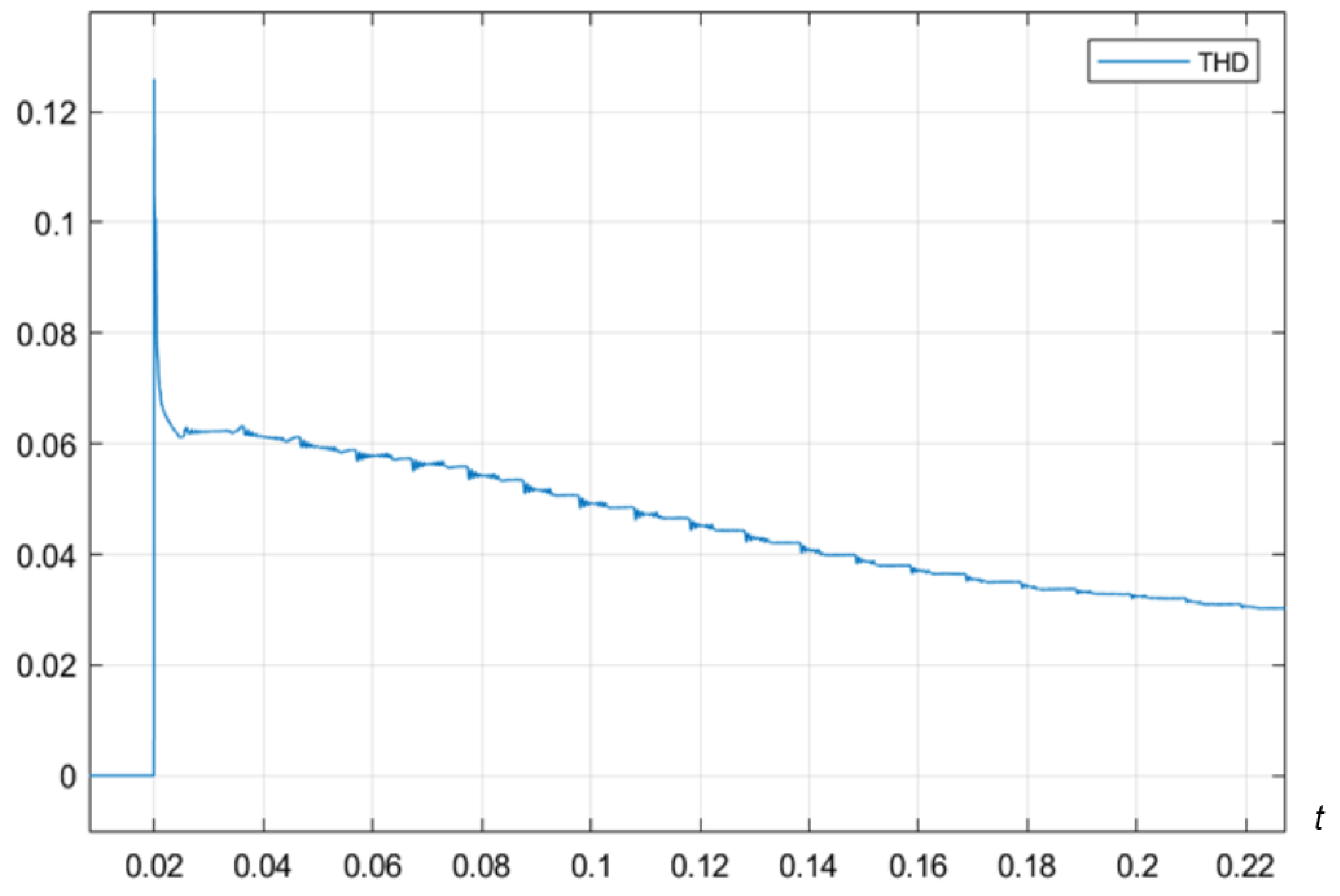
5.1. Simulation Results

The proposed LED driver circuit was modeled in MATLAB-Simulink®, and a circuit diagram was created, as shown in Figure 13.
The proposed LED driver consists of the integration of a modified Vienna rectifier and an isolated SEPIC–FLYBACK converter circuit. When the LED driver is connected to a 310 Vpp, 50 Hz AC source, the Vienna rectifier converts the AC voltage to a half-wave DC voltage. It maintains the constant output current with a PI controller that changes the voltage level by keeping the output current constant in variable loads to be connected to the circuit.
The circuit parameters of the recommended LED driver are given in Table 1.
In traditional converters, important parameters such as THD and PF cannot meet the mandatory standard values since the current drawn from the network is irregular in case of variable load. It is seen in Figure 14 that the proposed LED driver circuit provides these parameters.
An LED array of 18 watts and 0.6-ampere load is connected to the output of the proposed LED driver circuit. Figure 15 shows the total voltage level across switch S1. When the 220 Vrms voltage is applied to the circuit, and the output power is 18 W, the S1 switch closing voltage is around 70 V. Compared to other LED drivers, the switch stress is minimal.
To measure the harmonic level of the proposed LED driver, an FFT analysis program in Simulink® is used to measure the change in input current. The THD of the recommended LED driver is given in Figure 16.

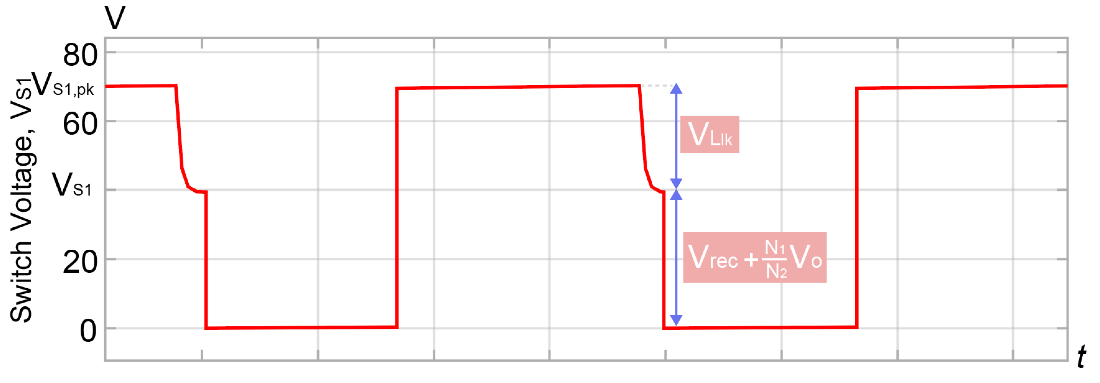
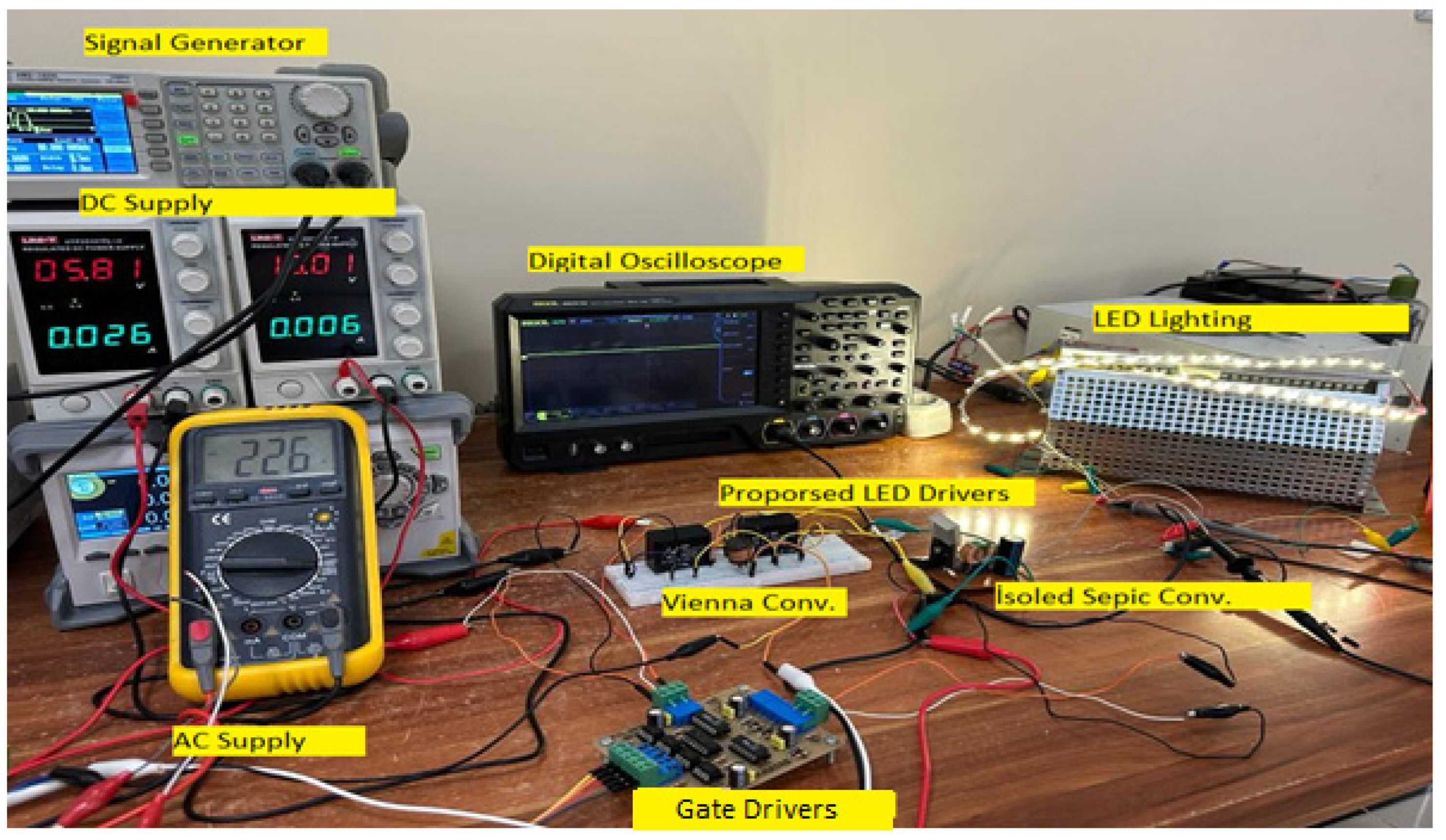
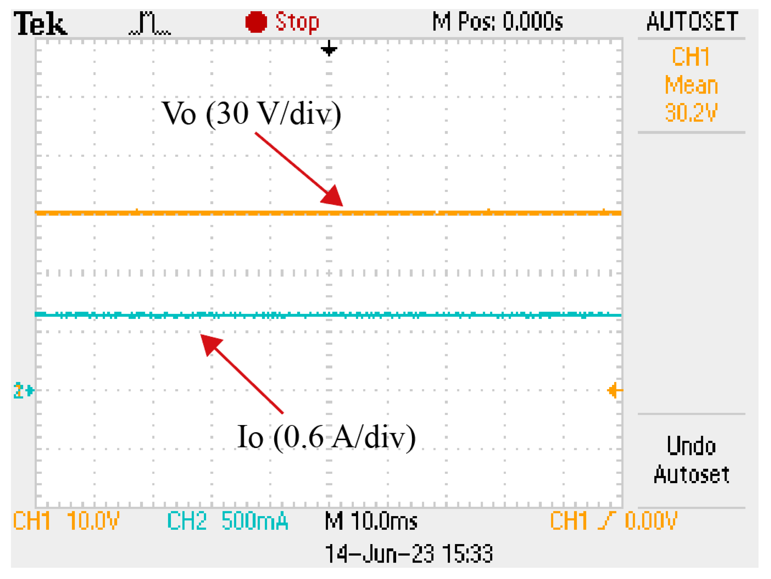
5.2. Experimental Results

To test the feasibility of the proposed LED driver circuit, a converter prototype was created, as shown in Figure 17.
When a 50 Hz, 220 RSM AC voltage is supplied to the input of the proposed LED driver, it provides a constant current of 30 V 0.6 A when a representative 50 ohm load is connected to the output of the circuit. A digital signal processor is used to drive the power switch of the prototype circuit. The designed driver maintains a constant output current of 0.6 Amps by adjusting the switch triggering signal to maintain a constant output current at variable loads. The models and values of the circuit elements used in the LED driver prototype are given in Table 2.
The proposed LED driver circuit has been experimentally realized, and the obtained results are presented in Figure 18. AC input current and voltage waveform of the circuit are given in Figure 18a, L1 inductor current and voltage waveform in Figure 18b, S1 switch voltage waveform in Figure 18d, diode current waveform in Figure 18e and output current and voltage waveform in Figure 18f.
As seen in Figure 18a, the current drawn and the voltage are in the same phase. As can be seen in Figure 18d, it is seen that the voltage of the S1 switch is at the level of 70 Volts at a power of 18 watts versus the input voltage of 220 Vrms. According to this result, the proposed LED driver circuit reduces the switch stress without using a snubber. It is seen that the simulation and experimental results overlap with each other.
The measured power factor of the proposed LED driver is given in Figure 19. Since the current and voltage are in the same phase in the driver circuit, the power factor of the circuit is measured as 0.97.
The power factor of the recommended LED driver is greater than 0.97, which complies with the Energy Star guideline.
The measured harmonic current level comparison of the IEC-61000-3-2 Class C standard and the proposed circuit is given in Figure 20.
As a result of the changes in the current drawn from the AC network, the total harmonic value of the circuit is measured. The THD value was measured using the Tektronix DPO4034 350 MHz Digital oscilloscope analyzer function. The measured THD of the recommended LED driver is below 4%. The measured value is lower than the IEC-61000-3-2 Class C limits.
A comparison of the simulation and experimental results is given in Table 3. As can be seen from the table, it has been observed that the simulation results and the experimental results overlap.
The oscilloscope image of the experimental result output current and voltage of the proposed LED driver circuit is shown in Figure 21.
The proposed LED driver gives an average output voltage of 30 V and a constant output current of 0.6 A at 18 W power and 50 ohm reference load. Table 3 compares the experimental and simulation results of the proposed circuit. As can be seen in Table 3, it was observed that the simulation and experimental results were close to each other.
A comparison of the proposed LED driver circuit with similar studies in the literature is presented in Table 4.
Table 4 shows that the 34 W LED driver has a high power factor of 0.99. In addition, while the efficiency is 82.3%, the output current fluctuation is very low at 18%. However, the switch overvoltage is more than twice the steady state voltage [24].
The 21 W–30 V output LED driver suggested by Poorali et al. has a high power factor of 0.99. Total harmonics meet IEC 61000-3-2 Class C standard, and fluctuation is 25%. High efficiency (with a value of 95%) is achieved using non-electrolytic capacitors in the driver circuit. However, since the switch-off voltage is three times the input voltage, the voltage stress on the switch is relatively high [25].
Ahmad et al. a suppressor circuit is designed to prevent switching stress and fluctuation in the input current in the AC–DC converter. The 18 W driver has a high power factor and an efficiency of more than 90%. However, the efficiency of the circuit is low due to the suppression circuit used in the circuit [26].
The switch voltage of the proposed circuits is about twice the input voltage. Switch stress can be reduced by using active inhibitors. However, since the use of these inhibitors will increase the number of elements in the circuit, circuit control will be difficult, and the cost will increase. This reduces the reliability of the recommended LED drivers.

6. Conclusions

The LED driver reduces the switching overvoltage caused by the parasitic leakage inductance of the high-frequency transformer in the isolated SEPIC converter without using a suppression circuit. In addition, with the controller designed in the circuit, it provides constant output current at different loads while maintaining important parameters such as 4% low THD and 0.97 high power factor. Thanks to the single-phase Vienna converter used in the circuit, the switching overvoltage has been reduced to as low as 70 volts compared to conventional rectifiers. Since the isolated SEPIC structure of the circuit provides isolation, its reliability is increased. Since the input current drawn from the network is in phase with the input voltage, the power factor is close to one. The use of a non-electrolytic output capacitor (CO), which reduces the fluctuation in the output voltage, contributes to the prolongation of the life of the designed LED driver. It has been observed that the efficiency of the circuit at variable loads is 97%. In simulation and experimental studies, the overvoltage on the switch was kept at a low voltage level of 70 volts. The proposed LED driver, compared to the isolated SEPIC with snubber, has an increased efficiency circuit since there is no switch stress-reducing element.

Author Contributions

Conceptualization, K.G.; methodology, K.G.; validation, K.G. and M.N.A.; formal analysis, K.G. and M.N.A.; supervision, M.N.A.; All authors have read and agreed to the published version of the manuscript.

Funding

This research received no external funding.

Institutional Review Board Statement

Not applicable.

Informed Consent Statement

Not applicable.

Data Availability Statement

Data are contained within the article.

Conflicts of Interest

The authors declare that they have no known competing financial interests or personal relationships that could have appeared to influence the work reported in this paper.

References

  1. Nazarudin, M.S.; Rahim, M.A.A.; Aspar, Z.; Yahya, A.; Selvaduray, T.R. A flyback SMPS LED driver for lighting application. In Proceedings of the 2015 10th Asian Control Conference: Emerging Control Techniques for a Sustainable World, ASCC 2015, Kota Kinabalu, Malaysia, 31 May–3 June 2015. [Google Scholar] [CrossRef]
  2. Zhang, S.; Wang, Y.; Liu, X.; Zhou, Y.; Xu, D. A single-switch integrated-stage LED driver based on Cuk and Class-E converter. In Proceedings of the 2018 International Power Electronics Conference, IPEC-Niigata—ECCE Asia 2018, Niigata, Japan, 20–24 May 2018; pp. 934–938. [Google Scholar] [CrossRef]
  3. Lamar, D.G.; Arias, M.; Rodriguez, A.; Fernandez, A.; Hernando, M.M.; Sebastian, J. Design-Oriented analysis and performance evaluation of a low-cost high-Brightness led driver based on flyback power factor corrector. IEEE Trans. Ind. Electron. 2012, 60, 2614–2626. [Google Scholar] [CrossRef]
  4. Cheng, C.-A.; Wu, H.-C. A Novel Single-Stage High-Power-Factor AC-DC LED Power Supply for Streetlight Applications. In Proceedings of the 2018 IEEE 7th Global Conference on Consumer Electronics, GCCE 2018, Nara, Japan, 9–12 October 2018; pp. 128–129. [Google Scholar] [CrossRef]
  5. Prieto, M.B.F.; Litran, S.P.; Aranda, E.D.; Gomez, J.M.E. New Single-Input, Multiple-Output Converter Topologies: Combining Single-Switch Nonisolated DC-DC Converters for Single-Input, Multiple-Output Applications. IEEE Ind. Electron. Mag. 2016, 10, 6–20. [Google Scholar] [CrossRef]
  6. Zareie, M.; Poorali, B.; Eren, S.; Pahlevani, M. A Power Factor Correction LED Driver With Direct Power Transfer Feature. IEEE J. Emerg. Sel. Top. Ind. Electron. 2021, 3, 988–997. [Google Scholar] [CrossRef]
  7. Luo, Q.; Huang, J.; He, Q.; Ma, K.; Zhou, L. Analysis and Design of a Single-Stage Isolated AC–DC LED Driver With a Voltage Doubler Rectifier. IEEE Trans. Ind. Electron. 2017, 64, 5807–5817. [Google Scholar] [CrossRef]
  8. Pouladi, F.; Farzanehfard, H.; Adib, E.; Le Sage, H. Single-Switch Soft-Switching LED Driver Suitable for Battery-Operated Systems. IEEE Trans. Ind. Electron. 2018, 66, 2726–2734. [Google Scholar] [CrossRef]
  9. Wang, Y.; Qiu, Y.; Xu, D. A single-stage LED driver based on resonant converter with low-voltage stress. In Proceedings of the 2018 IEEE Industry Applications Society Annual Meeting, IAS 2018, Portland, OR, USA, 23–27 September 2018. [Google Scholar] [CrossRef]
  10. Tian, G.; Qi, W.; Yan, Y.; Jiang, Y.Z. High power factor LED power supply based on SEPIC converter. IET Electron. Lett. 2014, 50, 1866–1868. [Google Scholar] [CrossRef]
  11. Cheng, C.-A.; Cheng, H.-L.; Chang, C.-H.; Chang, E.-C.; Kuo, Z.-Y.; Lin, C.-K.; Hou, S.-H. A Novel AC-DC LED Integrated Streetlight Driver with Power-Factor-Correction and Soft-Switching Functions. In Proceedings of the 2021 IEEE International Future Energy Electronics Conference (IFEEC), Taipei, Taiwan, 16–19 November 2021; IEEE: Piscataway, NJ, USA, 2021; pp. 1–3. [Google Scholar]
  12. Divya, K.M.; Parackal, R. High power factor integrated buck-boost flyback converter driving multiple outputs. In Proceedings of the IC-GET 2015–2015 Online International Conference on Green Engineering and Technologies, Coimbatore, India, 27 November 2015. [Google Scholar] [CrossRef]
  13. Kumar, K.A.; Veeramallu, V.S.; Narasimharaju, B. Performance Analysis of Coupled Inductor Based Ripple Free Boost PFC AC-DC LED Driver. In Proceedings of the 9th IEEE International Conference on Power Electronics, Drives and Energy Systems, PEDES 2020, Jaipur, India, 16–19 December 2020. [Google Scholar] [CrossRef]
  14. Wang, Y.; Huang, J.; Wang, W.; Xu, D. A single-stage single-switch LED driver based on integrated buck-boost circuit and Class E converter; A single-stage single-switch LED driver based on integrated buck-boost circuit and Class E converter. In Proceedings of the 2015 IEEE Industry Applications Society Annual Meeting, Addison, TX, USA, 18–22 October 2015. [Google Scholar] [CrossRef]
  15. Lam, J.; Jain, P.K. A novel isolated electrolytic capacitor-less single-switch AC-DC offline LED driver with power factor correction. In Proceedings of the Conference Proceedings—IEEE Applied Power Electronics Conference and Exposition—APEC, Fort Worth, TX, USA, 16–20 March 2014; pp. 1356–1361. [Google Scholar] [CrossRef]
  16. Chowdhury, D.; Hussain, M.I.; Zakaria, G.; Khan, Z.R. A low power LED driver with a soft-switched buck converter and a parallel-loaded series L-C resonant inverter. In Proceedings of the ICECE 2018—10th International Conference on Electrical and Computer Engineering, Dhaka, Bangladesh, 20–22 December 2018; pp. 26–29. [Google Scholar] [CrossRef]
  17. Wang, Y.; Huang, J.; Wang, W.; Xu, D. A Single-Stage Single-Switch LED Driver Based on Class-E Converter. IEEE Trans. Ind. Appl. 2016, 52, 2618–2626. [Google Scholar] [CrossRef]
  18. Hwu, K.I.; Yau, Y.T.; Lee, L.-L. Powering LED using high-efficiency SR flyback converter. IEEE Trans. Ind. Appl. 2010, 47, 376–386. [Google Scholar] [CrossRef]
  19. Lee, S.-W.; Do, H.-L. A Single-Switch AC-DC LED Driver Based on a Boost-Flyback PFC Converter with Lossless Snubber. IEEE Trans. Power Electron. 2017, 32, 1375–1384. [Google Scholar] [CrossRef]
  20. Yadav, V.K.; Verma, A.K.; Yaragatti, U.R. An Integrated Single Switch AC-DC System for LED Driven by an Unconventional Rectifier. In Proceedings of the 9th IEEE International Conference on Power Electronics, Drives and Energy Systems, PEDES 2020, Jaipur, India, 16–19 December 2020. [Google Scholar] [CrossRef]
  21. Yadav, V.K.; Verma, A.K.; Yaragatti, U. High PFC Integrated Stage Single Switch AC-DC System for LED Power Driver. In Proceedings of the 2021 International Conference on Sustainable Energy and Future Electric Transportation, SeFet 2021, Hyderabad, India, 21–23 January 2021. [Google Scholar] [CrossRef]
  22. Cheng, C.-A.; Cheng, H.-L.; Chang, E.-C.; Chang, C.-H.; Lai, S.-W.; Huang, P.-H. A single-switch LeD tube light driver with coupled-inductor and power-factor-correction for indoor lighting applications. In Proceedings of the 2020 International Symposium on Computer, Consumer and Control, IS3C 2020, Taichung City, Taiwan, 13–16 November 2020; pp. 240–242. [Google Scholar] [CrossRef]
  23. Yadav, V.K.; Verma, A.K.; Yaragatti, U.R. Modelling and control of two stage high PFC LED driver circuit using average current control method driven by vienna rectifier. In Proceedings of the PIICON 2020—9th IEEE Power India International Conference, Sonepat, India, 28 February–1 March 2020. [Google Scholar] [CrossRef]
  24. Somarowthu, P.R.R.; Saxena, S.K.; Mahajan, D.B. Isolated SEPIC Converter with a novel Voltage Clamp Circuit. In Proceedings of the 2018 IEEE International Conference on Power Electronics, Drives and Energy Systems, PEDES 2018, Chennai, India, 18–21 December 2018; Institute of Electrical and Electronics Engineers Inc.: Piscataway, NJ, USA, 2018. [Google Scholar] [CrossRef]
  25. Poorali, B.; Adib, E. Analysis of the Integrated SEPIC-Flyback Converter as a Single-Stage Single-Switch Power-Factor-Correction LED Driver. IEEE Trans. Ind. Electron. 2016, 63, 3562–3570. [Google Scholar] [CrossRef]
  26. Ahmad, S.; Tan, N.M.L.; Baharuddin, M.Z.; Buticchi, G. A High-Performance Isolated SEPIC Converter for Non-Electrolytic LED Lighting. IEEE Access 2021, 9, 149894–149905. [Google Scholar] [CrossRef]
Figure 1. Topology of a high-power factor LED driver with two-stage Vienna rectifier [23].
Electronics 12 04946 g001
Figure 2. A simplified switched circuit topology of the proposed circuit.
Electronics 12 04946 g002
Figure 3. Conventional Vienna rectifiers: (a) classic Vienna rectifier (b) modified Vienna rectifier.
Electronics 12 04946 g003
Figure 4. Modified Vienna rectifier operating modes: (a) positive alternance, (b) negative alternance.
Electronics 12 04946 g004
Figure 5. Capacitor coltages Cp, Cn.
Electronics 12 04946 g005
Figure 6. Vienna rectifier total output voltage.
Electronics 12 04946 g006
Figure 7. Mode I operating mode.
Electronics 12 04946 g007
Figure 8. Mode II operating mode.
Electronics 12 04946 g008
Figure 9. Mode III operating mode.
Electronics 12 04946 g009
Figure 10. (a)L1 inductor voltage–current plot of the proposed LED driver, S1 switch voltage–current plot. (b) C1 storage capacitor voltage–current graph, Lm magnetizing inductor voltage–current graph.
Electronics 12 04946 g010
Figure 11. Output diode Do voltage–current graph and output capacitor Co voltage–current graph of the proposed LED driver.
Electronics 12 04946 g011
Figure 12. Control loop of proposed LED driver.
Electronics 12 04946 g012
Figure 13. Recommended single-stage-isolated SEPIC–FLYBACK AC–DC LED driver circuit.
Electronics 12 04946 g013
Figure 14. Input and output simulation waveforms of the proposed LED driver circuit. (Vin input voltage, Iin current drawn, Vout output voltage, and Iout output current).
Electronics 12 04946 g014
Figure 15. Switch voltage (VS1) waveforms of LED driver circuit input and output.
Electronics 12 04946 g015
Figure 16. Measured harmonic current level (THD) of the recommended LED driver.
Electronics 12 04946 g016
Figure 17. Photograph of the experimental setup.
Electronics 12 04946 g017
Figure 18. The experimental waveform of the implemented prototype. (a) AC input current and voltage waveform; (b) L1 inductor current and voltage waveform (c) zoomed-in of L1 waveforms; (d) voltage waveform of switch S1; (e) diode current waveform; (f) output current and voltage waveform.
Electronics 12 04946 g018
Figure 19. Measured power factor of LED driver at recommended 18 W rated power.
Electronics 12 04946 g019
Figure 20. Comparison of the measured harmonic current level of the proposed circuit with the IEC-61000-3-2 Class C standard.
Electronics 12 04946 g020
Figure 21. Oscilloscope image of the output current and voltage of the prototyped circuit.
Electronics 12 04946 g021
Table 1. Circuit parameters of recommended LED driver.
ComponentSymbolValue
Input voltage (V)VinAC-310 Vpp
Filter capacitorCp, Cn10 (µF) 450 V AC
Filter inductorL500 µH
İnput inductorL12 mH
Storage capacitorC1100 (µF)
Output capacitor (µF)Co2200 (µF)
TransformerT1N2/N1 = 1
Output current (A)Io0.6 A
Output voltage (V)Vo30 V
Output power (W)W18 W
ResistorR50 Ω
Table 2. Model and ratings of the recommended LED driver.
ComponentSymbolModel PartRating
Input İnductorL22 × 14 × 8 1.0 diameter 10 A500 (µH)
Input CapacitorCp, CnP220M186JN10 uF 450VAC Capacitor CF505U37LL
Diode rectifierDp, Dn, 2x1N5408Repetitive Peak reverse voltage, VRRM = 1 kV
Storage İnductorL122 × 14 × 8 1.0 diameter 10 A2 mH
SwitchS1IRF740N-CHANNEL 400 V-0.48 ohm-10 A
Storage CapacitorC1F611DU335M40DC Voltage = 160 V
Output DiodeDo1N5408Repetitive Peak reverse voltage, VRRM = 1 kV
TransformationT-1:1
Output CapacitorCoR60DR522A402200 µH DC Voltage = 50 V
Table 3. Comparison of simulation and experimental results 220 Vrms and 18 W nominal operating condition.
SimulationExperiment
Peak Input Current (A)0.10.112
Power Factor0.9750.972
Odd Harmonics Value
3rd0.110.12
50.0540.06
70.0440.04
90.0260.029
110.0210.022
Average Output Current (A)0.6120.601
Average Output Voltage (V)30.12530.20
Peak Switch Voltage (V)7070.6
Table 4. Comparison of the proposed LED driver with other research-isolated SEPIC converters designed using a snubber circuit.
Component242526Proposed LED Driver
Input Voltage (V)22–32 Vac185–220 Vac90–240310 Vpp
Output Voltage (V)25.5303030
Output Power (W)34211818
Switching Frequency (kHz)-506050
Output Capacitor (µF)-10882200
Peak Efficiency82.3% at 34 W95% at 16.8 W93.56% at 18 W95% at 18 W
Power Factor0.98–0.990.990.93–0.9750.97
Overvoltage (V)150No overvoltage at turn-off, However, peak voltage is high8230
Steady-state Voltage (V)70 at 32 V input voltage600 at 220 v input voltage286 at 150 V input voltage310 Vpp input voltage
Snubber TypePassivePassivePassivePassive
Snubber Component Count1 Capacitor
1 Diode
1 Inductor
2 Capacitor
2 Diode
1 Inductor
2 Capacitor
2 Diode
-
Flicker (%)1818--
Disclaimer/Publisher’s Note: The statements, opinions and data contained in all publications are solely those of the individual author(s) and contributor(s) and not of MDPI and/or the editor(s). MDPI and/or the editor(s) disclaim responsibility for any injury to people or property resulting from any ideas, methods, instructions or products referred to in the content.

