Abstract
In order to analyze the interference mechanisms of indirect lightning effects on a low-noise amplifier (LNA), a circuit model of the LNA was constructed based on the advanced design system 2020 (ADS 2020) software. Lightning pulse injection simulations were conducted to explore the influence of lightning pulses on the performance of the LNA. A pin injection test was performed to investigate the interference and damage threshold of the LNA. A protective circuit incorporating the transient voltage suppressor (TVS) and Darlington structure was designed through simulation, employing the ADS 2020 for the LNA. The research findings reveal that the interference threshold for the LNA is 60 V, while the damage threshold is determined to be 100 V. The protective circuit demonstrates a measured insertion loss of 0.1 dB, a response time of 1.5 ns, and a peak output voltage of 20 V. The research results indicate that the protective circuit can effectively reduce the impact of lightning’s indirect effects on the LNA. In the future, we will continue the design work of the protective circuit and proceed with physical fabrication and experimental validation.
1. Introduction
It is inevitable for aircraft to encounter lightning strikes during flight. According to the International Air Transport Association (IATA), commercial aircraft have a potential risk of being struck by lightning approximately once every 10,000 flight hours [1]. The increasing complexity of the electromagnetic environment within aircraft can be attributed to the utilization of composite materials in contemporary aircraft structures, as well as the continuous expansion of onboard electronic systems [2,3]. Additionally, the existence of an external lightning environment presents a heightened potential for adversely impacting the performance of the electronic equipment installed onboard [4]. The effects of lightning on aircraft are categorized into direct and indirect effects. The direct lightning effects refer to the physical consequences caused by the direct attachment of the lightning channel to the aircraft [5]. The indirect lightning effects pertain to the interference caused by the coupling of the lightning environment with onboard electronics. Excessive voltage and current can induce disruptions in RF circuits and signal interfaces, consequently impacting signal transmission and potentially resulting in permanent equipment failure.
The low-noise amplifier (LNA), serving as a crucial component of communication receivers, is positioned at the forefront of the RF receiving link. The primary function of the LNA is to amplify the weak signals received from satellites to increase the reception range. Additionally, it determines the sensitivity of the receiver [6]. The nonlinear degradation of the LNA caused by an electromagnetic pulse (EMP) was investigated. The experimental results demonstrated that the real-time response and RF characteristics of the LNA showed nonlinear and permanent degradation features under the jamming of an EMP [7]. An empirical investigation was conducted to examine the effects of EMP radiation on the LNA [8], which illustrates that the semiconductor characteristics of the LNA make it more susceptible to interference. A high-performance electromagnetic protection circuit, based on the LC filter and transient voltage suppressor (TVS) diodes, was proposed in [9]. However, it was discovered that the power capacity of the protection circuit may be limited or insufficient. In [10], a high-intensity radiated-field (HIRF) protection circuit utilizing PIN diodes was introduced and subsequently validated through experimental verification. A protection circuit for a high-altitude electromagnetic pulse (HEMP) was designed based on heterojunction bipolar transistors in [11]. A comparison between two types of TVS diodes was conducted in [12], which obtained the relationship between dynamic resistance and input power. Based on the conducted analysis, five distinct topologies were designed for high-power microwave (HPM) protection. In [13], a dc–dc pulse-width modulation buck–boost converter was safeguarded against lightning’s indirect effects through the implementation of a metal oxide varistor and a series inductive blocking element. A protection circuit was devised by integrating iron core inductors and metal oxide varistors to provide protection against indirect lightning effects in avionic environments [14].
Prior academic contributions have indeed proposed design solutions for protective circuits against EMPs. However, with limitations associated with size, power capacity, and response time, these designs are not sufficiently suitable for effectively protecting the LNA against lightning pulses. In this paper, we evaluated the response characteristics of the LNA when exposed to lightning pulses and proposed a protective circuit for the LNA. The major contributions of our work are as follows [15,16]:
- We devised a circuit schematic for the LNA and conducted a lightning pulse injection simulation. We analyzed the variations in the gain and current values of the LNA under various conditions of lightning pulse injections.
- A pin injection test was conducted to evaluate the LNA’s transient susceptibility. Consequently, we ascertained the interference threshold and damage threshold of the LNA.
- We designed a lightning protection circuit specifically for the LNA, which can shield it from the indirect effects of lightning while not interrupting its normal operations. It is designed by combining TVS diodes and Darlington structures. TVS diodes are employed to trigger the conduction of the Darlington structures that are utilized to discharge the current.
The rest of this article is organized as follows. Section 2 provides an analysis of the waveform and power spectrum of the lightning pulses. Section 3 establishes an LNA circuit model and performs pulse injection simulations. Section 4 performs transient susceptibility experiments to investigate the effects of lightning induction. Section 5 presents the design of a protective circuit. Finally, Section 6 concludes this article.This research investigates the interaction mechanism of lightning pulses on the LNA, offering references and theoretical support for lightning’s indirect effects testing and protection measures of the LNA.
2. Methodology
This section presents the methodology employed in this study to analyze the interference mechanisms of indirect lightning effects on the LNA and propose an effective protective circuit design. The framework of the proposed method is illustrated in Figure 1. The research methodology encompasses the LNA circuit model design, lightning pulse data processing, LNA sensitivity analysis, and protective circuit design. This comprehensive approach allowed for a systematic analysis of the interference mechanisms and facilitated the development of an effective protective circuit design to mitigate the impact of indirect lightning effects on the LNA [17].

Figure 1.
Framework of the proposed method.
2.1. LNA Circuit Model Design
The LNA circuit was simulated using advanced design system 2020 (ADS 2020), with the GaAs PHEMT serving as the core component. Initially, a DC scan analysis was performed to determine the appropriate static operating point for the LNA. Subsequently, bias circuits were designed based on the identified static operating point. Following the principles of minimum noise and maximum gain, the input matching circuit and output matching circuit of the LNA were meticulously crafted. Moreover, to enhance circuit stability, a negative feedback circuit was incorporated between the source and gate of the LNA.
2.2. Lightning Pulse Data Processing
2.2.1. Lightning Pulse
Investigating the characteristics of the lightning pulse and spectrum enables a comprehensive analysis of the pulse in the time and frequency domains. This facilitates the examination of the interference mechanisms caused by lightning pulses on the LNA, as well as subsequent pulse injection simulations. SAE ARP 5412B defines the voltage waveform that characterizes the external lightning conditions encountered by aircraft. It also establishes a standardized transient voltage waveform that is anticipated to occur on wire bundles and equipment ports. For the purpose of analyzing lightning pulses, this study employs a damped sinusoidal wave to simulate the resonant oscillation voltage generated on cables due to the interaction between electric or magnetic fields and apertures [18]. The waveform of the damped sinusoidal wave is illustrated in Figure 2a. The mathematical expression of the damped sinusoidal wave is:
where represents the peak coefficient, represents the peak voltage, and represents the damping coefficient, where = 0.231f, = 2f, and f = 1 MHz.
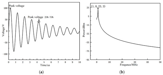
Figure 2.
Lightning pulse and power spectrum: (a) Time-domain waveform of the lightning pulse; (b) power spectrum of the lightning pulse.
2.2.2. Power Spectrum Conversion
The damped sinusoidal wave was transformed into a power spectrum to analyze the energy distribution of the lightning pulse, which facilitated the subsequent simulation of injected lightning pulses. The time-domain signal, denoted as f(t), can be converted into its spectral representation through the process of Fourier transformation, as illustrated in (2) [19].
The energy and average power of the signal can be expressed as follows:
The ℘() is defined as the power spectrum of the signal, which characterizes the distribution of power across various frequencies. It provides the frequency-domain characteristics of the signal. Consequently, the power of the signal can be determined as follows:
Based on (4) and (5), the power spectrum of the signal can be derived as:
where T represents the period of the signal and F(j) represents the frequency spectrum of the signal.
According to (8), the power spectrum of the lightning pulse with a peak voltage of 100 V is depicted in Figure 2b. The analysis reveals that the energy of the lightning pulse is primarily concentrated at 1 MHz. Furthermore, it is observed that the distribution of power is solely dependent on the peak voltage of the lighting pulses.
2.3. LNA Sensitivity Analysis
2.3.1. Pulse Injection Simulation
To assess the interference conditions of the LNA under indirect lightning effects, a pulse injection simulation was conducted. This simulation involved applying both the lightning pulse and RF signals to the input port of the LNA using a power combiner. The objective of this simulation was to analyze the transient response and performance of the LNA when subjected to lightning-induced pulses. The transient simulation provided insights into the dynamic behavior and effects of lightning pulses on the LNA, while the power scan analysis established the interference threshold and characterized the LNA’s robustness against lightning-induced stress levels. The results from these simulations contributed to a comprehensive understanding of the LNA’s susceptibility to interference and facilitated the development of effective protective measures.
2.3.2. Pin Injection Test
To investigate the interference condition of the LNA and evaluate its resilience to lightning-induced interference, a pin injection test was conducted. This test involved injecting lightning pulses directly into the LNA circuit using pin probes. The primary objective was to meticulously monitor and analyze crucial parameters, including the LNA’s output power, as well as the input and output currents, across various peak lightning pulse injection scenarios. Additionally, an in-depth calculation of the LNA’s gain during the test was performed. The pin injection test provided invaluable insights into the LNA’s response to lightning-induced interference, thereby facilitating the determination of both the interference and damage thresholds.
2.4. Protective Circuit Design
The protective circuit design for the LNA was developed using ADS software. It incorporates a combination of TVS diodes and Darlington structures to ensure reliable surge protection. The TVS diodes serve the purpose of clamping the output voltage and triggering the conduction of the Darlington structures, while the Darlington structures are responsible for the current’s dissipation. The design process involved optimizing the performance of the protective circuit by appropriately adjusting the clamping voltage of the TVS diodes. This adjustment was critical in achieving the desired conduction of the Darlington current dissipation circuit, thereby reducing the response time of the protective circuit and enhancing its power capacity.
3. Pulse Injection Simulation
3.1. Circuit Mode of the LNA
Figure 3a shows the physical diagram of the LNA. Within the core component of the LNA, highlighted by the red circle, lies a pseudomorphic high-electron-mobility transistor (GaAs PHEMT). The aforementioned chip offers advantages such as high electron mobility, high gain, and low noise, rendering it highly suitable for the amplification of small signals. The circuit of the LNA was modeled utilizing ADS 2020, as shown in Figure 3b [20]. The primary objective of this research is to analyze the L1 band of the GPS satellite, which operates at a frequency of 1575 MHz [21]. According to the datasheet of ATF54143, the LNA was designed to operate with a drain-source voltage of 4V and a drain-source current of 65 mA. This configuration ensured that the gain and noise figures were compliant with the design requirements. Additionally, a biasing circuit was designed for the LNA. The design of the impedance-matching circuit was tailored to the operating frequency of the LNA. The input matching circuit was designed based on the principle of minimum noise matching, while the output matching circuit followed the principle of maximum gain matching.

Figure 3.
Circuit model of the LNA: (a) Physical diagram of the LNA; (b) schematic diagram of the LNA.
The input port of the LNA was configured with an excitation signal. Harmonic balance analysis and transient simulation controls were incorporated to obtain the noise figure, input voltage (), and output voltage (). The gain of the LNA was calculated according to (9).
Figure 4a shows the simulation results of the LNA. The LNA exhibited a gain of 18.3 dB and a noise figure of 0.34 dB at a frequency of 1575 MHz. Figure 4b depicts the gate current, source current, and drain current of the LNA. During typical operation, the gate current of the LNA exhibited fluctuations around 0 A, whereas the source current and drain current remained equal and fluctuated around 25 mA.
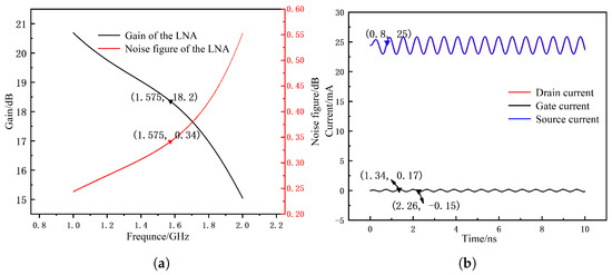
Figure 4.
Simulation results of the LNA: (a) gain and noise figure of the LNA; (b) gate current, source current, and drain current of the LNA.
3.2. Simulation of the Interference Effects
In order to accurately simulate the coupling process of lightning and effectively demonstrate its interference effect, a power combiner was utilized to simultaneously inject the lightning pulse and RF signal into the input port of the LNA. A high-power single-pulse with a frequency of 1 MHz was employed to replicate the lightning pulse, while a small-signal wave at 1575 MHz was used to simulate the RF signal of the LNA [22]. The small-signal wave was modulated by a square wave with a pulse width of 10 ns, a pulse power of −30 dBm, and a period of 10 ns. The high-power single-pulse exhibited a pulse width of 2 ns and a period of 20 ns. To evaluate the influence of power levels on the LNA, a comprehensive analysis was performed by sweeping the power of the high-power pulse [23]. The variation in the gain with pulse power is shown in Figure 5.

Figure 5.
The gain of the LNA varies with the injected pulse power.
It was apparent that the amplification of the LNA decreased when the injected pulse power exceeded 9 dBm. This can be attributed to the nonlinear effects of the LNA, which represent a deviation from linearity in which the output signal of the amplifier no longer maintains a direct proportionality to its input signal. When the injected power exceeded 32 dBm, it exceeded the simulation range. According to (8), the high-power single-pulse with a power of 9 dBm corresponds to an attenuated sinusoidal waveform with a peak voltage of 30 V. Similarly, the pulse with a power level of 32 dBm corresponds to a peak voltage of 270 V.
The RF susceptibility testing procedures in RTCA DO-160G are widely applied to airborne equipment in the indirect lightning effects research field. According to RTCA DO-160G, the test level should be determined based on the installation environment of the LNA and the exposure level of its interconnected cables [24]. Therefore, the lightning pulse peak voltages ranging from 0 to 300 V were sampled with a step size of 10 V. The power of the high-power single-pulse at 1 MHz was calculated utilizing the sampled peak voltage values. The high-power single-pulse injection simulations were conducted based on the calculated power values. Figure 6a illustrates the currents of the LNA when a high-power single-pulse with a power level of 3.3 dBm (equivalent to a lightning pulse with a peak voltage of 10 V) was injected. Following pulse injection, the gate current experienced a rapid increase to 2.2 mA, while the drain and source currents simultaneously rose to 63.6 mA, maintaining equality. The currents returned to their initial state after a time interval of 6.6 ns.
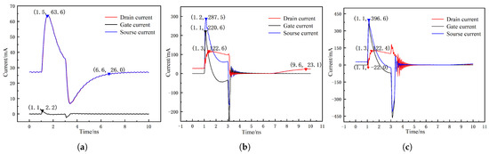
Figure 6.
Gate current, source current, and drain current of the LNA: (a) The peak voltage of the lightning pulse is 10 V; (b) the peak voltage of the lightning pulse is 50 V; (c) and the peak voltage of the lightning pulse is 100 V.
Progressive augmentation of the injection power resulted in a gradual convergence of the gate current and source current in the LNA. Specifically, when a high-power single-pulse power of 18.3 dBm (equivalent to a lightning pulse with a peak voltage of 50 V) was applied, both the gate current and source current exhibited a significant increase compared to the previous stage, as depicted in Figure 6b. A disconnection between the gate and the source resulted in the formation of a low-impedance pathway. The LNA current returned to normal within a time period of 9.6 ns. When a high-power single-pulse with a power level of 23.3 dBm (equivalent to a lightning pulse with a peak voltage of 100 V) was injected, a strong correlation between the gate current and source current was observed. As shown in Figure 6c, reversal was observed in the drain current at 1.1 ns. A breakdown between the gate and drain forms a low-impedance path. Following pulse cessation, the currents failed to return to their initial state, indicating that the LNA suffered irreversible damage.
3.3. Analysis of Results
According to the pulse injection simulation, the damage evaluation curve of the LNA is shown in Figure 7. The LNA operated normally, with a steady gain of 18.3 dB when the power level of the injected pulse was less than 9 dBm. The gain of the LNA decreased, and the current recovery time progressively prolonged as the injected power exceeded 9 dBm. Surpassing a power level of 18.6 dBm, the LNA demonstrated recoverable damage, characterized by the emergence of a low-impedance path between the gate and source terminals. Observably, the LNA sustained irreversible damage, discernible as a low-impedance path between the gate and drain terminals when the power level exceeded 23.3 dBm. The interference mechanism of lightning pulses on the LNA operates as follows: The LNA achieves amplification by regulating the gate voltage, thereby controlling the two-dimensional electron gas between the drain and source terminals. Simultaneously, a short circuit forms between the source and drain terminals. Meanwhile, the gate remains non-conductive to both the source and drain, exhibiting a negligible gate current [7]. As the injected pulse power escalates, both the gate current and source current surge, consequently compromising the gain of the LNA. A subsequent augmentation in power thus results in an overcurrent across the gate’s metallic band, leading to both a gate–source and gate–drain breakdown [25,26].
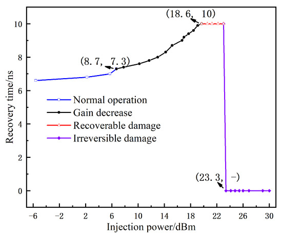
Figure 7.
Damage evaluation curve of the LNA.
4. Lightning-Induced Transient Susceptibility
4.1. Experiment Platform
To validate the simulation results and scrutinize the effects of genuine lightning pulses on the LNA, we adhered to the guidelines in Section 22 of RTCA DO-160G and performed a pin injection test to assess the transient sensitivity of the LNA [27]. The pin injection test is an experimental method that directly applies the produced transient signals to the signal pins of the device. This test was utilized to assess the LNA’s fault tolerance capabilities. Figure 8a illustrates the schematic diagram of the pin injection test for the LNA, while Figure 8b shows the experimental platform.
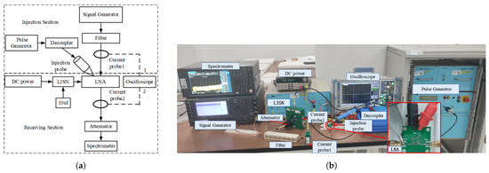
Figure 8.
Lightning-induced transient susceptibility of the LNA: (a) Schematic diagram of the LNA pin injection test; (b) lightning pulses injection experiment platform.
The types and functions of the test equipment are presented in Table 1. The testing platform comprises two sections: injection and receiving. The injection section encompassed a pulse generator, a vector signal generator, a filter, and an injection probe. The receiving section included a DC power supply, a line impedance stabilization network (LISN), an oscilloscope, two current loops, an attenuator, and a spectrum analyzer. The filter operates within the frequency range of 1570–1580 MHz, exhibiting an insertion loss of 1 dB, while the attenuator was calibrated to provide a 10 dB attenuation [28].

Table 1.
Types and functions of the test equipment.
4.2. Experimental Results
To reflect the actual operating conditions of the LNA, the vector signal generator produced a modulated RF signal, operating at a power level of −30 dBm and a frequency of 1575 MHz. The output power of the LNA, which was monitored utilizing a spectrum analyzer, is depicted in Figure 9. The gain of the LNA can be calculated based on the input and output powers utilizing the following formula:
where represents the power of the RF signal, represents the power of the output signal, represents the in-band loss of the filter, and represents the attenuation of the attenuator. The gain of the LNA was calculated to be 15.8 dB.
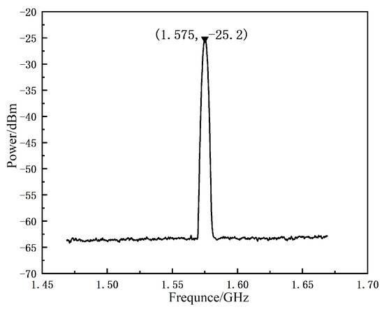
Figure 9.
Output power of the LNA.
To evaluate the effects of lightning pulses on the LNA, a pin injection test was performed by incrementally increasing the peak voltage of the lightning pulses in 10 V increments. The evaluation of the effects of lightning pulses on the LNA was based on the variations in LNA gain, input current, and output current. Each test was repeated a minimum of five times to ensure the validity and precision of the results. The relationship between the LNA’s gain and the peak voltage of injected pulses is presented in Table 2. There was no significant change in the LNA gain when the peak voltage of the pulse was set to 10 V. The input and output currents of the LNA are illustrated in Figure 10a, indicating that the output current significantly surpasses the input current. LNA1, LNA3, LNA4, and LNA5 exhibited significant gain degradation when the peak voltage of the injected pulse was 60 V. Similarly, LNA2 exhibited evident gain degradation when the peak voltage reached 70 V [29]. The input and output currents of the LNA are depicted in Figure 10b, showing the input current approaching the output current. This finding aligns with the trends of the gate and source variations observed in the simulation results. After cessation of the pulse injection, the gain of the LNA recovered to approximately 16 dB, suggesting that the LNA experienced recoverable damage. LNA1, LNA3, and LNA5 demonstrated a rapid shift towards negative gains when the peak voltage of the injected pulse was 100 V. Identical behavior was observed in LNA2 and LNA4 when the pulse peak voltage reached 110 V. Following the cessation of the pulse injection, the gains of the LNAs could not recover, indicating permanent damage to the LNA. When the GaAs PHEMT chip of the LNA was replaced, the gain of the LNA recovered to 15.8 dB, demonstrating that the main cause of the lightning pulse damage to the LNA was the damage to the GaAs PHEMT chip [30].
Table 2.
The gain of the LNA varies with the peak voltage.
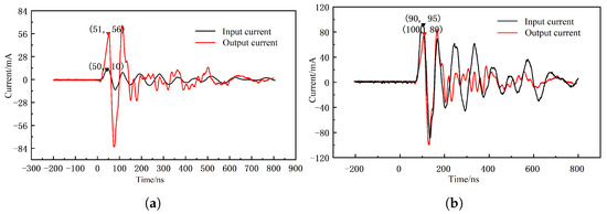
Figure 10.
Input current and output current of the LNA: (a) The LNA is undisturbed; (b) the gain of the LNA is significantly reduced.
The experimental results exhibit significant consistency across various samples under identical pulse injection conditions. Coupling lightning pulses into the LNA leads to a reduction in gain. Specifically, the LNA’s gain experiences a significant decrease when the peak voltage of the pulse exceeds 60 V. Additionally, the input current and output current of the LNA are nearly equal, impeding its effective functioning. When the peak voltage of the pulse exceeds 100 V, it results in irreversible damage to the GaAs PHEMT chips. The interference and damage patterns on the LNA caused by lightning pulses, as observed in the pin injection tests, aligned with the simulation results. The gain of the LNA decreases while the peak voltage of the injected lightning pulse increases. Furthermore, the gate current and source current progressively increase and approach equality. The phenomenon of gate–source breakdown and gate–drain breakdown occurs while the pulse level exceeds the threshold voltage. However, the damage threshold obtained from the simulation is marginally lower than the experimental damage threshold. This discrepancy can be attributed to the simulation process, which evaluates the LNA disturbance based on the alterations in the gate, source, and drain currents of the LNA. In practical scenarios, the device is susceptible to damage only when its temperature exceeds a specific melting point [31].
5. Protection Circuit of the LNA
5.1. Design of the Protection Circuit
Based on the simulation and experimental results, it is imperative to design a protective circuit for the LNA. The protective circuit is required to provide effective protection against lightning pulses while simultaneously minimizing any potential interference with the reception of RF signals by the LNA. Surge protection devices, including gas discharge tubes (GDT), TVS diodes, and voltage-dependent resistors (MOV), are typically incorporated for protective purposes [32]. GDT and MOV devices, despite their high power capacity, are limited by their extended response times and larger parasitic capacitance [33]. TVS diodes, in contrast, exhibit shorter response times and smaller parasitic capacitance, albeit with a lower power capacity [34]. The Darlington structure, on the other hand, provides the advantage of reduced parasitic capacitance and excellent protection against electromagnetic pulses. Therefore, this paper proposes a protective circuit that integrates TVS diodes and Darlington pairs in parallel, as illustrated in Figure 11. The protective circuit is comprised of two stages, purposefully designed to re-route currents and confine voltage within a secure range. The first stage consists of two series-connected bidirectional TVS diodes, D1 and D2. The clamping voltage of D2 operates as the trigger voltage for the second stage. The output voltage of the protection circuit corresponds to the cumulative clamping voltages of D1 and D2. The second stage includes two parallel-connected Darlington structures, which enhance the dissipation capacity. The Darlington structure primarily comprises a field-effect transistor (FET) and a high-power bipolar transistor.The device selection method for protective circuits is shown in Appendix A.
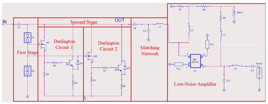
Figure 11.
Lightning pulses protection circuit of the LNA.
5.2. Simulation of the Protection Circuit
To verify the effectiveness of the protection circuit, we conducted transient and S-parameter simulations, applying a 100 V peak voltage lightning pulse at the input port of the protection circuit. The input and output voltages of the protection circuit are shown in Figure 12a. Significantly limiting the peak output voltage to 20 V—lower than the input voltage—the protection circuit demonstrated effective protection. The S-parameter and the voltage standing-wave ratio (VSWR) of the protection circuit are depicted in Figure 12b. The protective circuit exhibited an insertion loss of 0.106 dB and a VSWR of 1.017 at a frequency of 1575 MHz, indicating that it had a negligible effect on the LNA.
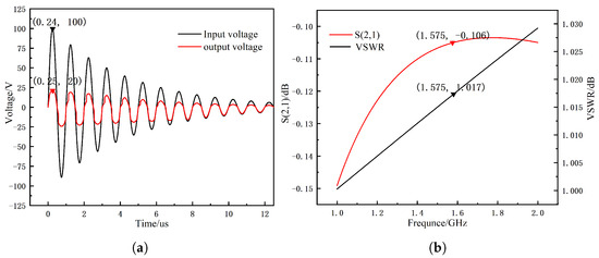
Figure 12.
Simulation results of the protection circuit: (a) Input voltage and output voltage of the protection circuit; (b) S-parameter and VSWR of the protection circuit.
To verify the current dissipation capability of the protective circuit, high-power single-pulse injections were carried out for the proposed protection circuit, TVS protection circuit, and parallel TVS-MOV protection circuit [35]. The power level for the injection was set at 23.3 dBm. The response time and output power of the protective circuit are depicted in Figure 13. The protective effects of different circuits are presented in Table 3. The proposed protection demonstrates superior power handling capabilities, while its response time is comparable to that of the TVS protection circuit. When compared to the parallel TVS-MOV protection circuit, the proposed protection configuration shows significant advancements in response time and power capacity.
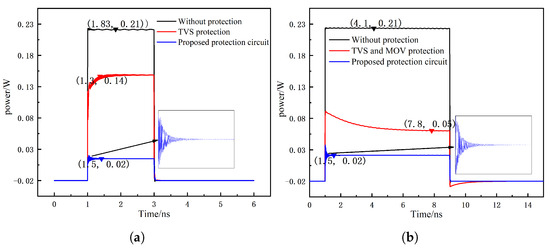
Figure 13.
Protection effect of different protection circuits: (a) Comparison with TVS protection circuit; (b) comparison with parallel TVS diodes-MOV protection circuit.
Table 3.
Comparison of protective circuit effects.
6. Conclusions
This paper conducted pulse injection simulations and transient sensitivity tests to investigate the impact of lightning-induced transients on the LNA. Based on the observed interference patterns, a protective circuit of the LNA was devised. The primary findings of the research are as follows:
- (1)
- The coupling of lightning pulses with the LNA leads to a decrease in gain. Exceeding the predetermined damage thresholds, the LNA experiences gate–source and gate–drain breakdown.
- (2)
- Recoverable damage occurs to the LNA when the peak voltage of the coupled lightning pulse surpasses 60 V. Conversely, when the peak voltage surpasses 100 V, the GaAs PHEMT chip sustains irreversible damage.
- (3)
- The protection circuit exhibits a response time of 1.5 ns, ensuring that the output voltage remains below 20 V. This effectively mitigates the interference caused by lightning pulses without interrupting normal operations.
Author Contributions
Conceptualization, Z.M. and Z.D.; methodology, C.S.; software, J.L.; validation, Z.M., J.L. and Z.D.; formal analysis, J.L.; investigation, J.L.; resources, C.S.; data curation, Z.M.; writing—original draft preparation, J.L.; writing—review and editing, Z.M.; visualization, C.S.; supervision, Z.D.; project administration, Z.M.; funding acquisition, S.H. All authors have read and agreed to the published version of the manuscript.
Funding
This research received no external funding.
Data Availability Statement
The data presented in this study are available on request from the corresponding author.
Conflicts of Interest
The authors declare no conflict of interest. The funders had no role in the design of the study; in the collection, analyses, or interpretation of data; in the writing of the manuscript; or in the decision to publish the results.
Appendix A. Selection of the Protection Circuit
In this appendix, we provide a detailed description of the simulation stages, parameters, and selection criteria used in the design of the proposed protective circuit for mitigating the indirect effects of lightning on low-noise amplifiers. The simulation was conducted using ADS 2020, and the parameters were selected based on component specifications and system requirements.
Appendix A.1. Simulation Stages
The protection circuit simulation involves the following stages:
Appendix A.1.1. Stage 1: TVS Diode Configuration
The first stage comprises two series-connected bidirectional TVS diodes, D1 and D2. The purpose of this stage is to suppress transient voltage spikes and limit the voltage across the subsequent stage. During normal operation, the TVS diodes present high impedance and do not significantly affect the signal passing through the protective circuit. However, when a high-voltage transient occurs, the TVS diodes rapidly switch to a low-impedance state, effectively clamping the voltage and limiting its amplitude. The clamping voltage of D2 is set to operate as the trigger voltage for the second stage.
Appendix A.1.2. Stage 2: Darlington Structure Configuration
The second stage of the protective circuit incorporates two parallel-connected Darlington structures, which further enhance the dissipation capacity and improve the overall protection performance. Each Darlington structure consists of a high-power bipolar transistor and a field-effect transistor (FET). The Darlington structure provides improved current amplification and voltage regulation capabilities. The FET serves as a voltage-controlled current source, while the bipolar transistor amplifies the current. This configuration enables efficient dissipation of high currents and helps maintain the voltage across the protected circuitry within a safe range.
Appendix A.2. Parameters
The following parameters were considered during the simulation and selection of the protective circuit components:
Appendix A.2.1. TVS Diode D1
- Breakdown voltage (VBR): 30 V
- Clamping voltage (VC): 17 V
- Peak pulse current (IPP): 10 A
- Junction capacitance (CJ): 10 pF
- Reverse standoff voltage (VRWM): 25 V
- Peak pulse power dissipation (PPPM): 500 W
- Clamping voltage at peak pulse current: 17 V
- Clamping voltage at peak pulse power: 18 V
Appendix A.2.2. TVS Diode D2
- Breakdown voltage (VBR): 30 V
- Clamping voltage (VC): 3 V
- Peak pulse current (IPP): 5 A
- Junction capacitance (CJ): 10 pF
- Reverse standoff voltage (VRWM): 15 V
- Peak pulse power dissipation (PPPM): 200 W
- Clamping voltage at peak pulse current: 3 V
- Clamping voltage at peak pulse power: 5 V
Appendix A.2.3. FET
- Drain–source breakdown voltage (BVDS): 50 V
- Drain–source on-resistance (RDS(on)): 0.1
- Gate–source threshold voltage (VGS(th)): 2.5 V
- Junction capacitance (CJ): 10 pF
- Maximum drain current (IDmax): 10 A
- Maximum power dissipation (PDmax): 2 W
- Input capacitance (Ciss): 100 pF
- Response time: <1 ns
Appendix A.2.4. Bipolar Transistor
- Collector–emitter breakdown voltage (BVCE): 60 V
- Collector current (IC): 5 A
- Base-emitter voltage (VBE): 1.2 V
- Maximum power dissipation (PDmax): 2 W
- Current gain (hFE): 100
- Output capacitance (Cobo): 5 pF
Appendix A.3. Selection Criteria
The selection of components for the protective circuit was based on the following criteria:
Appendix A.3.1. Voltage Rating
Consider the voltage rating of the components in the protective circuit. Ensure that the breakdown voltage of the TVS diodes, the drain–source breakdown voltage of the FET, and the collector–emitter breakdown voltage of the bipolar transistor are higher than the maximum expected voltage that the circuit will encounter during normal operation or transient events.
Appendix A.3.2. Clamping Voltage
The clamping voltage of the TVS diodes should be below the maximum acceptable voltage level for the protected circuitry. Consider the clamping voltages of both D1 and D2 TVS diodes to ensure they are within an acceptable range.
Appendix A.3.3. Peak Pulse Current
Evaluate the peak pulse current (IPP) rating of the TVS diodes. The selected TVS diodes should have a peak pulse current rating that can handle the expected current surges during transient events. Ensure the peak pulse current rating is higher than the maximum current expected in the protected circuit.
Appendix A.3.4. Response Time
Consider the response time of the protective components, such as the TVS diodes, FET, and bipolar transistor. A fast response time, typically specified as less than 1 ns, is desirable to ensure the rapid clamping of voltage spikes and transient events.
References
- Yoshikawa, E.; Ushio, T. Tactical decision-making support information for aircraft lightning avoidance: Feasibility study in area of winter lightning. Bull. Am. Meteorol. Soc. 2019, 100, 1443–1452. [Google Scholar] [CrossRef]
- Guoru, D.; Jiachen, S.; Haichao, W.; Yutao, J. Disscussion on technologies of intelligent spectrum management and control under complex electro magnetic environments. Acta Aeronaut. Astronaut. Sin. 2021, 42, 200–212. [Google Scholar]
- Zhenyang, M.; Jing, Z.; Chunlei, S.; Jiacheng, F.; Xuhong, L. Test and optimization of shield effectiveness for airborne electronic equipment. Acta Aeronaut. Astronaut. Sin. 2020, 41, 32. [Google Scholar]
- Kim, Y.; Jo, J.; Kim, D.; Lee, H.; Myong, R. Effects of lightning on UAM aircraft: Complex zoning and direct effects on composite prop-rotor blade. Aerosp. Sci. Technol. 2022, 124, 107560. [Google Scholar] [CrossRef]
- Ishimoto, K.; Tossani, F.; Napolitano, F.; Borghetti, A.; Nucci, C.A. LEMP and ground conductivity impact on the direct lightning performance of a medium-voltage line. Electr. Power Syst. Res. 2023, 214, 108845. [Google Scholar] [CrossRef]
- Vignesh, R.; Gorre, P.; Kumar, S. A novel wide bandwidth FBSSIR integrated low-noise amplifier for satellite navigational receiver system. Microelectron. J. 2021, 117, 105288. [Google Scholar] [CrossRef]
- Yu, X.; Ma, Z.; Chai, C.; Shi, C.; Wang, P. Nonlinear and permanent degradation of GaAs-based low-noise amplifier under electromagnetic pulse injection. IEEE Trans. Electromagn. Compat. 2019, 62, 101–107. [Google Scholar] [CrossRef]
- Mansson, D.; Thottappillil, R.; Backstrom, M.; Lunden, O. Vulnerability of European Rail Traffic Management System to Radiated Intentional EMI. IEEE Trans. Electromagn. Compat. 2008, 50, 101–109. [Google Scholar] [CrossRef]
- Jingqi, Z.; Feng, Q.; Yuan, G.; Shouhong, Z. Design and experiment of wideband electromagnetic pulse protection circuit with effective suppression capability. High Power Laser Part. Beams 2023, 35, 023004. [Google Scholar]
- Deng, B.; Lin, M.; Zhang, J.; Wu, Z.; Liu, C.; Liu, P. PIN-Diode-Based High-Intensity Radiation Fields (HIRF) Protection of a Printed Dipole Antenna. IEEE Trans. Electromagn. Compat. 2021, 63, 198–205. [Google Scholar] [CrossRef]
- Hao, R.; Zhang, X.; Gao, H.; Wu, H.; Cheng, J.; Li, G.P. A novel high-altitude electromagnetic pulse (HEMP) protection circuit for RF applications. Microelectron. J. 2019, 84, 1–8. [Google Scholar] [CrossRef]
- Zhang, C.R.; Zeng, X.; Zhou, L.; Mao, J.F. Protection Effects Using Transient Voltage Suppressor Diodes Based Circuits Under High-Power Microwave Pulses. IEEE Trans. Electromagn. Compat. 2021, 63, 2058–2064. [Google Scholar] [CrossRef]
- Rimal, H.P.; Reatti, A.; Corti, F.; Lozito, G.M.; Antonio, S.Q.; Faba, A.; Cardelli, E. Protection From Indirect Lightning Effects for Power Converters in Avionic Environment: Modeling and Experimental Validation. IEEE Trans. Ind. Electron. 2021, 68, 7850–7862. [Google Scholar] [CrossRef]
- Faba, A.; Rimal, H.P. Robust Lightning Indirect Effect Protection in Avionic Diagnostics: Combining Inductive Blocking Devices With Metal Oxide Varistors. IEEE Trans. Ind. Electron. 2018, 65, 6457–6467. [Google Scholar] [CrossRef]
- Khan, H.; Hussain, T.; Khan, S.U.; Khan, Z.A.; Baik, S.W. Deep multi-scale pyramidal features network for supervised video summarization. Expert Syst. Appl. 2024, 237, 121288. [Google Scholar] [CrossRef]
- Khan, H.; Haq, I.U.; Munsif, M.; Mustaqeem; Khan, S.U.; Lee, M.Y. Automated wheat diseases classification framework using advanced machine learning technique. Agriculture 2022, 12, 1226. [Google Scholar] [CrossRef]
- Alnajim, A.M.; Habib, S.; Islam, M.; Albelaihi, R.; Alabdulatif, A. Mitigating the Risks of Malware Attacks with Deep Learning Techniques. Electronics 2023, 12, 3166. [Google Scholar] [CrossRef]
- SAE ARP 5412B: 2013; Aircraft Lightning Environment and Related Test Waveforms. SAE International: Warrendale, PA, USA, 2013.
- Kang, J.; Ju, H.; Liu, L. Comparison of response transmissibility and power spectral density transmissibility on operational modal analysis. Mech. Syst. Signal Process. 2021, 160, 107912. [Google Scholar] [CrossRef]
- Bei-jun, P.; Mao-zheng, C.; Hao-hui, W.; Hao, Y.; Yun-wei, N. Design of 4–40 GHz Ultra-wideband Low Noise Amplifier for Radio Astronomy. Chin. Astron. Astrophys. 2022, 46, 515–528. [Google Scholar] [CrossRef]
- Yu, X.; Cao, X.; Wang, J.; Ge, Y.; Shen, F. The benefit of B1C/B2a signals for BDS-3 wide-area decimeter-level and centimeter-level point positioning with observable-specific signal bias. Measurement 2023, 214, 112815. [Google Scholar] [CrossRef]
- Wang, L.; Chai, C.C.; Li, F.X.; Qin, Y.; Yang, Y.T. Influence of gate voltage dependent piezoelectric polarization on damage effect of GaN HEMT induced by high power electromagnetic pulse. Microelectron. Reliab. 2022, 136, 114665. [Google Scholar] [CrossRef]
- Yuqin, F.; Erwei, C.; Mini, W.; Qinglong, Z.; Yazhou, C. Analysis of damage effect of higlrpower microwave bomb on GNSS receiver. Syst. Eng. Electron. 2020, 42, 37–44. [Google Scholar]
- Xinhai, Y.; Zhenyang, M.; Chunlei, S.; Peng, W. Experiment study and failure analysis of lightning indirect effect of an airborne VHF communication station. Telecommun. Eng. 2018, 58. [Google Scholar]
- Liu, L.; Du, Z. Influence of microwave pulse power on the burnout effect of the AlGaN/GaN HEMT in a LNA. In Proceedings of the 2019 IEEE 6th International Symposium on Electromagnetic Compatibility (ISEMC), Nanjing, China, 1–4 November 2019; pp. 1–5. [Google Scholar]
- Zhang, C.; Zhang, J.; Wang, H.; Du, G. Burnout properties of microwave pulse injected on GaAs PHEMT. Microelectron. Reliab. 2015, 55, 508–513. [Google Scholar] [CrossRef]
- Filik, K.; Hajder, S.; Masłowski, G. Multi-stroke lightning interaction with wiring harness: Experimental tests and modelling. Energies 2021, 14, 2106. [Google Scholar] [CrossRef]
- Huang, X.; Wang, Y.; Chen, Y. Analysis of Electromagnetic Interference Effect of the Pulse Interference on the Navigation Receiver. Int. J. Antennas Propag. 2022, 2022, 1–12. [Google Scholar] [CrossRef]
- Huang, L.; Mao, Q.; Xiang, Z.; Zhu, D.; Meng, J. Destructive Testing for Reliability Analysis at High Power Microwave in GaAs/InGaP Hetero junction Bipolar Transistor. IEEE Trans. Device Mater. Reliab. 2023, 23, 198–203. [Google Scholar] [CrossRef]
- Huang, K.; Zhang, L.; Li, R.; Tian, Y.; He, Y.; Jiang, J.; Deng, X.; Su, W. A Compact Hybrid G-band Heterodyne Receiver Integrated with Millimeter Microwave Integrated Circuits and Schottky Diode-Based Circuits. Electronics 2023, 12, 2806. [Google Scholar] [CrossRef]
- Mao, Q.; Huang, L.; Xiang, Z.; Zhu, D.; Meng, J. High-power microwave pulse induced failure on InGaP/GaAs heterojunction bipolar transistor. Microelectron. Reliab. 2022, 139, 114848. [Google Scholar] [CrossRef]
- Zhong, S.; Qin, F.; Gao, Y.; Yan, Z. Response Characteristics of Gas Discharge Tube to High-Power Microwave. IEEE Access 2021, 9, 111486–111492. [Google Scholar] [CrossRef]
- Staikos, E.T.; Peppas, G.D.; Tsovilis, T.E. Wide Frequency Response of Varistors and Coordination With Transient Voltage Suppression Diodes. IEEE Trans. Power Deliv. 2022, 38, 453–462. [Google Scholar] [CrossRef]
- Qin, F.; Chen, W.; Wang, X.; Huang, T.; Cui, Z.; Nie, X. Transient response characteristics of metal oxide arrester under high-altitude electromagnetic pulse. Energies 2022, 15, 3303. [Google Scholar] [CrossRef]
- Kim, S.Y.; Park, J.S.; Lee, W.S. Development and Verification of Indirect Lightning-Induced Transient Protection Circuit for Avionics System. Appl. Comput. Electromagn. Soc. J. 2021, 36, 670–675. [Google Scholar] [CrossRef]
Disclaimer/Publisher’s Note: The statements, opinions and data contained in all publications are solely those of the individual author(s) and contributor(s) and not of MDPI and/or the editor(s). MDPI and/or the editor(s) disclaim responsibility for any injury to people or property resulting from any ideas, methods, instructions or products referred to in the content. |
© 2023 by the authors. Licensee MDPI, Basel, Switzerland. This article is an open access article distributed under the terms and conditions of the Creative Commons Attribution (CC BY) license (https://creativecommons.org/licenses/by/4.0/).