Abstract
This paper presents a high resolution delta-sigma modulator for continuous acquisition of electroencephalography (EEG) signals. The third-order single-loop architecture with a 1-bit quantizer is adopted to achieve 22.3-bit resolution. The effects of thermal noise on the performance of the delta-sigma modulator are analyzed to reasonably allocate the switched-capacitor sizes for optimal signal to noise ratio (SNR) and minimum chip area. The coefficients in feedback path and input path are optimized to avoid the signal distortion under the full-scale input voltage range with almost no increase in total capacitance sizes. Fabricated in 0.5 µm CMOS technology and powered by a 5 V voltage supply, the proposed delta-sigma modulator can achieve 136 dB peak SNR with 16 Hz input and 137 dB dynamic range in 100 Hz signal bandwidth with an oversampling ratio of 512. The modulator dissipates 700 µA. The core chip area is 1.96 mm. The modulator occupies 1.41 mm and the decimator occupies 0.55 mm.
1. Introduction
The monitoring of biopotential signals is a key and important component of the medical diagnostic system. Electroencephalography (EEG) waves are currently one of the most commonly used biopotential signals for monitoring brain activity [1]. In the analog-front-end (AFE) circuits of the whole system, ADCs are used to collect and digitize EEG signals. However, there are some challenges in ADC design. First, the EEG signals have extremely low frequency behavior and low signal amplitude (i.e., 0.5–70 Hz and 1–100 µV for surface EEG [2]). They are very susceptible to various aggressors, such as 1/f noise from CMOS transistors, power line interference, and thermal noise [3]. Second, dry electrodes with high impedance are preferred for continuous monitoring of brain signals [4], which will result in weaker EEG signal and lower common-mode-rejection-ratio (CMRR) due to mismatches. Additionally, charge accumulation caused by the natural humidity of dry electrodes can lead to the electrode-offset-voltage (EOV) of ±200–300 mV [5]. The large EOV will result in saturation of the integrator so as to affect the resolution of the modulator. Therefore, to achieve stable and accurate measurement of EEG signals, high resolution and large input voltage range ADCs are required.
Compared with other ADC structures, the delta-sigma ADC is promising for the application to convert EEG signals with higher resolution performance in the low frequency range [6]. Oversampling technology is employed to reduce quantization noise and noise shaping technology is used to push the noise to higher frequency bands. Then, a digital decimation filter is used to filter out the shaped noise in the high frequency domain, so as to achieve high conversion resolution. Due to the low power consumption and high integration, the delta-sigma ADCs have also proven their practicality in biomedical applications [7]. For example, a continuous-time delta-sigma modulator using a modified instrumentation amplifier and current reuse DAC for neural recording is proposed in [8], with the peak signal to noise and distortion ratio (SNDR) of 78 dB and the dynamic range (DR) of 90 dB are achieved for a bandwidth of 250 Hz. In [9], a low-power delta-sigma modulator with a low-noise amplifier in the first integrator is proposed, which can achieve a measured 96 dB DR, over a 250 Hz signal bandwidth, with an oversampling ratio (OSR) of 500.
There are three common ways to boost the SNR and SNDR of a delta-sigma modulator. First, increase the OSR with higher sampling frequency . But this will result in more power consumption. Second, increase the order of the loop filter in the single-loop structure to achieve more effective noise shaping (NS). But this will increase the circuit complexity and degrade the loop stability. Compared with the single-loop structure, the multistage noise-shaping (MASH) can ensure loop stability with higher NS order [10,11]. However, due to PVT variations, the mismatch of the transfer function between analog and digital domains can lead to quantization-error leakage and reduce conversion resolution. The third method is to increase the resolution of the quantizer, but multi-bit architecture requires the dynamic element matching (DEM) technique, which also requires extra current consumption for the extra blocks and increases the circuit complexity.
Taking the above conditions into consideration, this paper presents a single-loop third-order structure with a single-bit quantizer to achieve a delta-sigma modulator with 136 dB SNR for EEG monitoring. In addition, the thermal noise effects are analyzed for minimum total capacitance and the modulator coefficients are optimized to avoid distortion of the integrator in the full-scale input range. As a result, the proposed modulator has a higher overload level, which is good for expanding the dynamic range in the EEG acquisition system.
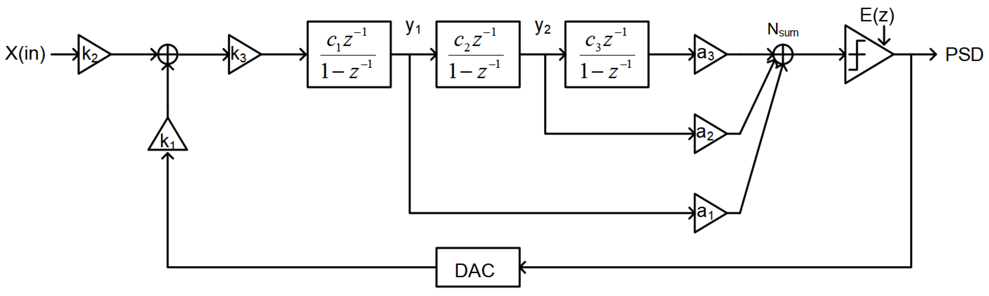
2. Thermal Noise Analysis and Proposed Topology Design
In this section, topology architectural design of the proposed high-resolution delta-sigma modulator is discussed. It is essential to analyze the thermal noise effects in the delta-sigma loop before the topology design, so as to properly allocate the switched-capacitor sizes for optimal SNR and minimum chip area. Considering the second-order modulator loop using the feedforward topology shown in Figure 1 and Figure 2, we shall find the minimum acceptable capacitor sizes that satisfy a specified SNR by the following steps.
Figure 1.
Noise sources in the feedforward topology.
Figure 2.
Schematic of the feedforward topology.
Identify the main thermal noise sources of the modulator circuit, including the first integrator, the second integrator, and the adder circuit in front of the quantizer.
Find the PSD of the noise generated by each thermal noise source. The mean-square value of the input-referred noise voltage of the first integrator can be expressed as
Here, the parameter x = . The noise power at the input of the second integrator can be expressed as
In the adder circuit, the noise power of the three switched-capacitor branches can be equivalently represented as
Here, , and are ratioed. Since all these sources produce sampled white noise, the PSD of the jth source can be given by
Find the noise transfer function (NTF) from each noise source to the output. The integrator block can be denoted by
The NTF from the input of the first integrator to the output of the modulator is given by
The NTF from the input of the second integrator to the output is given by
The NTF from the output of the second integrator to the output of the modulator is given by
Integrate each noise PSD in the frequency band of interest. If OSR≫ 1, the resulting output noise powers are
Calculate the sum of all these contributions. With x = 0.1 in the expressions for and , the total output thermal noise power is
With OSR = 512 in this design, the can be simplified as
This expression shows that in the first integrator dominates the total output thermal noise power; and can be ignored because the noise of these capacitors is shaped by first-order and second-order high-pass transfer functions.
After the above analysis, an important optimization can be performed to minimize the sampling capacitance for a desirable thermal noise level according to
where is the amplitude of a half-scale signal. The capacitors in the other switched-capacitor structures can be chosen to be much smaller than .
Figure 3 shows the optimized single-loop third-order delta-sigma modulator topology. The integrator coefficients and feedforward coefficients are optimized with significant benefits in terms of silicon area and load capacitance. The feedforward paths are all summed at the input node of a comparator. Values and are used to amplify the feedback and input signals, so that the detected input signal range of the modulator can reach full scale. In order to avoid the signal distortion at the output of the first integrator, the amplified difference between input and feedback signals is scaled down by . Therefore, with , , and , the proposed delta-sigma modulator can achieve high SNR over the full-scale input range of 0 V to 5 V with almost no increase in total capacitance sizes. The NTF of the designed modulator can be calculated as
The coefficients of the designed modulator are summarized in Table 1. The ideal output spectrum, obtained with a behavioral simulation, is shown in Figure 4. With OSR of 512, the simulated SNDR at 16 Hz is 145.8 dB.
Figure 3.
Proposed single-loop third-order modulator topology.
Table 1.
Coefficients of the designed modulator.
Figure 4.
Ideal output spectrum with a 16 Hz input signal.
3. Circuit Implementation
This section describes some of the issues that need to be considered before circuit design, such as the integrator output swings, the OTA requirements, and the single-bit quantizer design. Then, the complete circuit-level implementation of the proposed modulator is explained.
3.1. Integrator Output Swings
As the proposed modulator is optimized to avoid signal distortion under full-scale input signal range, it is necessary to simulate the output voltage swing of each integrator. The behavioral simulation is performed with a full-scale input, and the output swing of each integrator after the input normalized to the reference voltage is shown in Figure 5. As we can see in this figure, the output swing of the first integrator is the largest, but it still does not exceed 60% of the reference voltage, which means that there will be no signal distortion with full-scale input signal.
Figure 5.
Integrator output swings with a 16 Hz full-scale input signal. (a) Output of the first integrator. (b) Output of the second integrator. (c) Output of the third integrator.
3.2. OTA Requirements
The OTA is a key component of the delta-sigma modulator and determines its main performance. The requirements for OTA mainly include DC gain, output swing, and gain bandwidth (GBW). The output swing determines the maximum input amplitude , which is very important for the dynamic range (DR) of a KT/C noise dominated modulator.
Therefore, a larger output swing allows for a reduction in sampling capacitance, thus reducing power consumption and chip area. In addition, the OTA DC gain must have sufficient margin for the process variations to avoid circuit performance fluctuations of the modulator. Figure 6 shows the relationship between SNR and OTA gains in the proposed topology. We can see that if the gain is above 50 dB, the wide variation does not affect the SNR significantly. The SNR starts to fall bellow 130 dB when the OTA gain is lower than 30 dB. But this gain requirement only takes into account noise shaping; higher OTA gain is required for better distortion performance in practical applications.
Figure 6.
The SNR versus the OTA gains.
A typical full-differential two-stage amplifier with a common-mode feedback (CMFB) circuit is employed in the modulator to achieve guaranteed circuit performance. The schematic is shown in Figure 7. Transistors PM0, NM0, and PM5 form the amplifier’s first stage to provide high DC gain. PM3 and NM3 form the second stage to provide large output voltage swing. PM4, NM4, and PM6 form the CMFB circuit to sense the output common-mode voltage and provide the control voltage to balance the OTA’s positive and negative outputs. R1A and R1B are the feedback resistors. R0 and C0 form the Miller compensation for stabilizing the OTA.
Figure 7.
Schematic of the OTA in the modulator.
It should be noted that the thermal noise and flicker noise of the first OTA is not shaped by the loop filter, and it directly influences the modulator performance. Particularly, the 1/f noise is dominant in very low frequency. Therefore, the input devices PM0A and PM0B, the main noise contributors, are designed with large dimension and large in order to suppress the OTA noise below the modulator overall noise floor. The other OTAs are relatively less critical than the first OTA; therefore, the current and performance are scaled down to reduce power consumption. From the post-layout typical simulation, the first OTA achieves 108 dB DC gain, 55° phase margin, and 13 MHz GBW with a 100 pF load. The other two OTAs achieve 98 dB DC gain, 12.5 MHz GBW, and 65° phase margin with a 100 pF load. The first and other OTAs draw 340A and 100A, respectively.
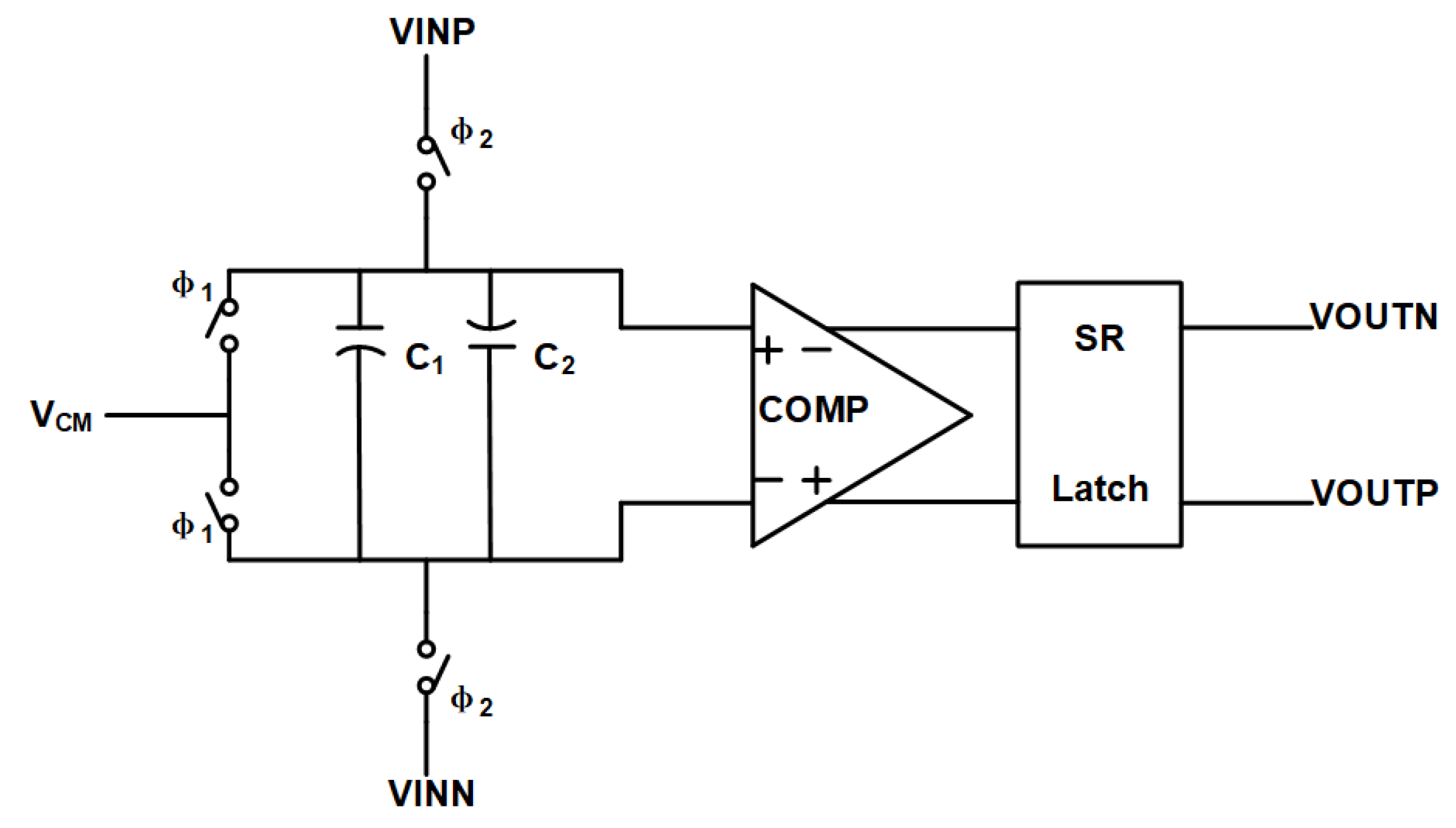
3.3. Single-Bit Quantizer Circuit
Figure 8 shows the single-bit quantizer circuit, including a dynamic comparator and an SR latch. At phase , the input of the comparator is reset to . Then, the differential signals at the summation node in Figure 3 are compared at phase . Two equal capacitors are connected in parallel, and the plates of and are opposite in order to achieve matching of the mim capacitors.
Figure 8.
Schematic of the single-bit quantizer.
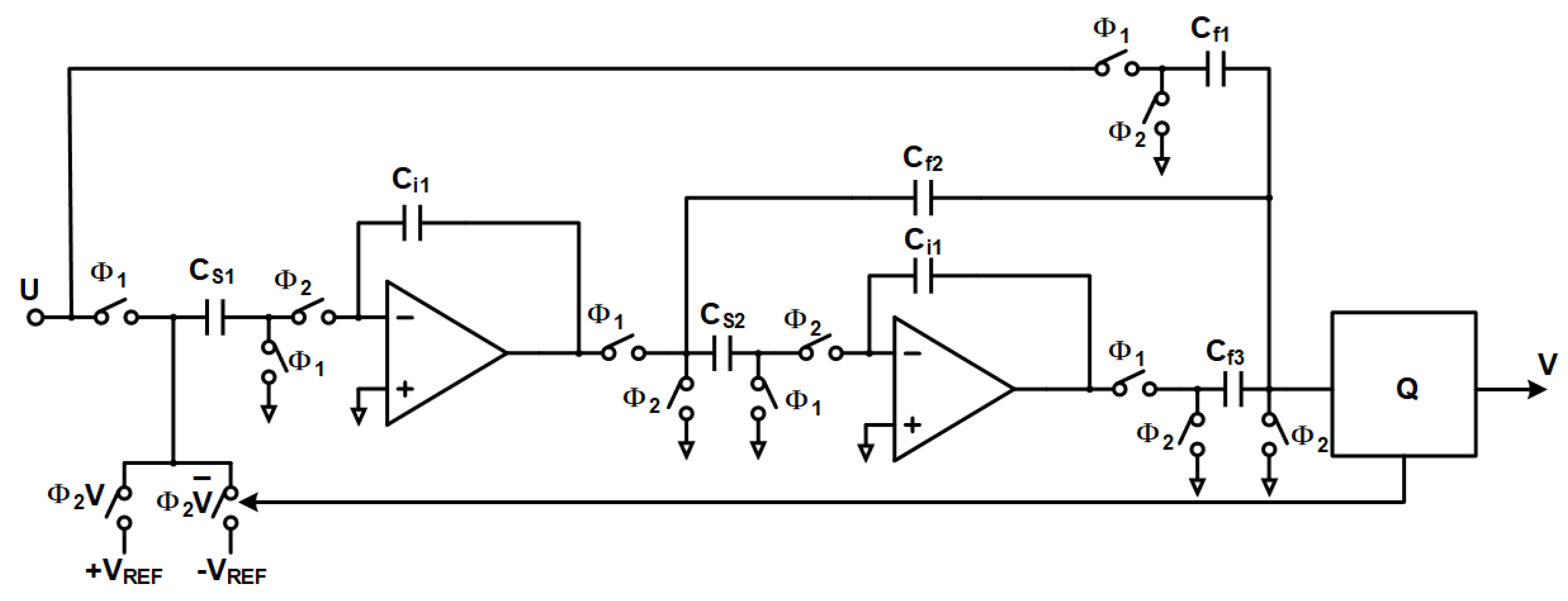
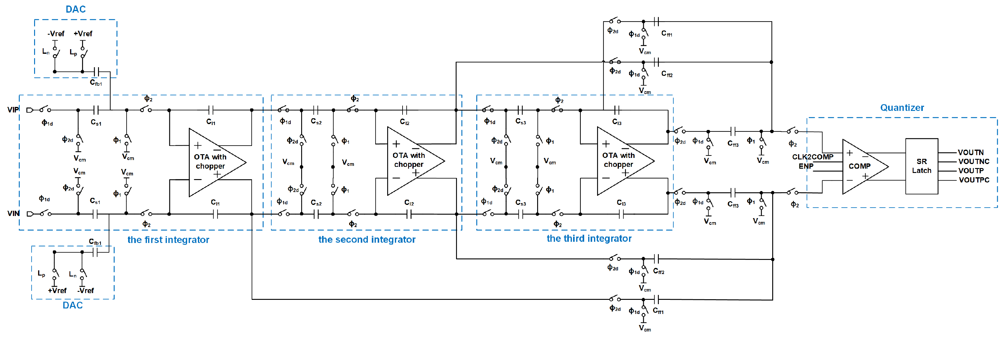
3.4. Complete Modulator Circuit Implementation
Figure 9 shows the complete circuit implementation of the proposed modulator. In order to improve the common mode noise rejection and avoid performance degradation, a fully differential circuit topology is adopted throughout the design [12]. The input signal is sampled during ; the voltage difference between the input and is stored in the sampling capacitors. Depending on the digital output of the quantizer, Lp or Ln will be opened and feedback reference levels will be applied to the sampling capacitors, which will perform the subtraction operation and then transfer charge from the sampling capacitors to the integration capacitors to complete the integration function during . The gain coefficients of the proposed modulator in Figure 3 are easily realized by appropriate capacitance sizes.
Figure 9.
Schematic of the presented third-order modulator.
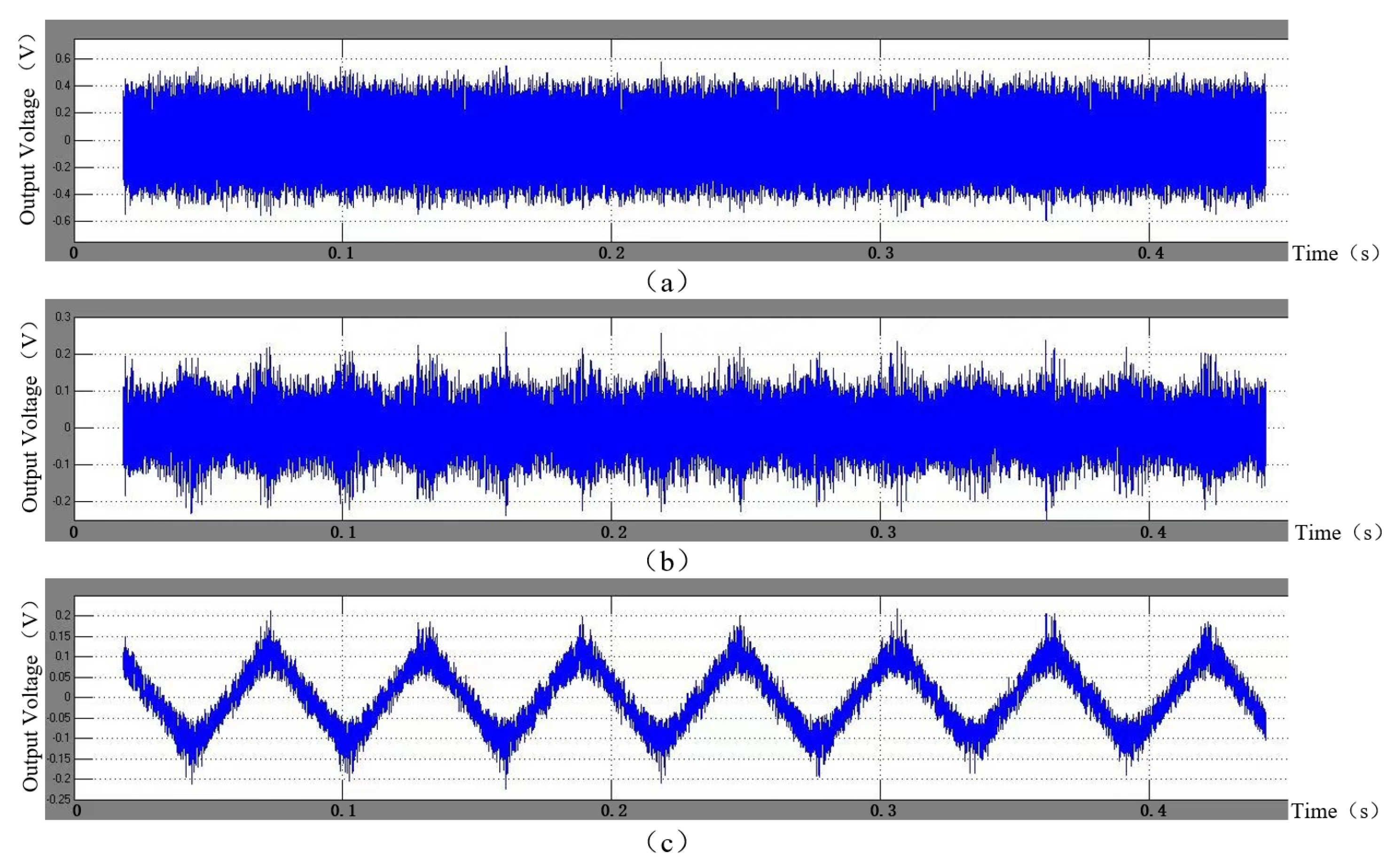
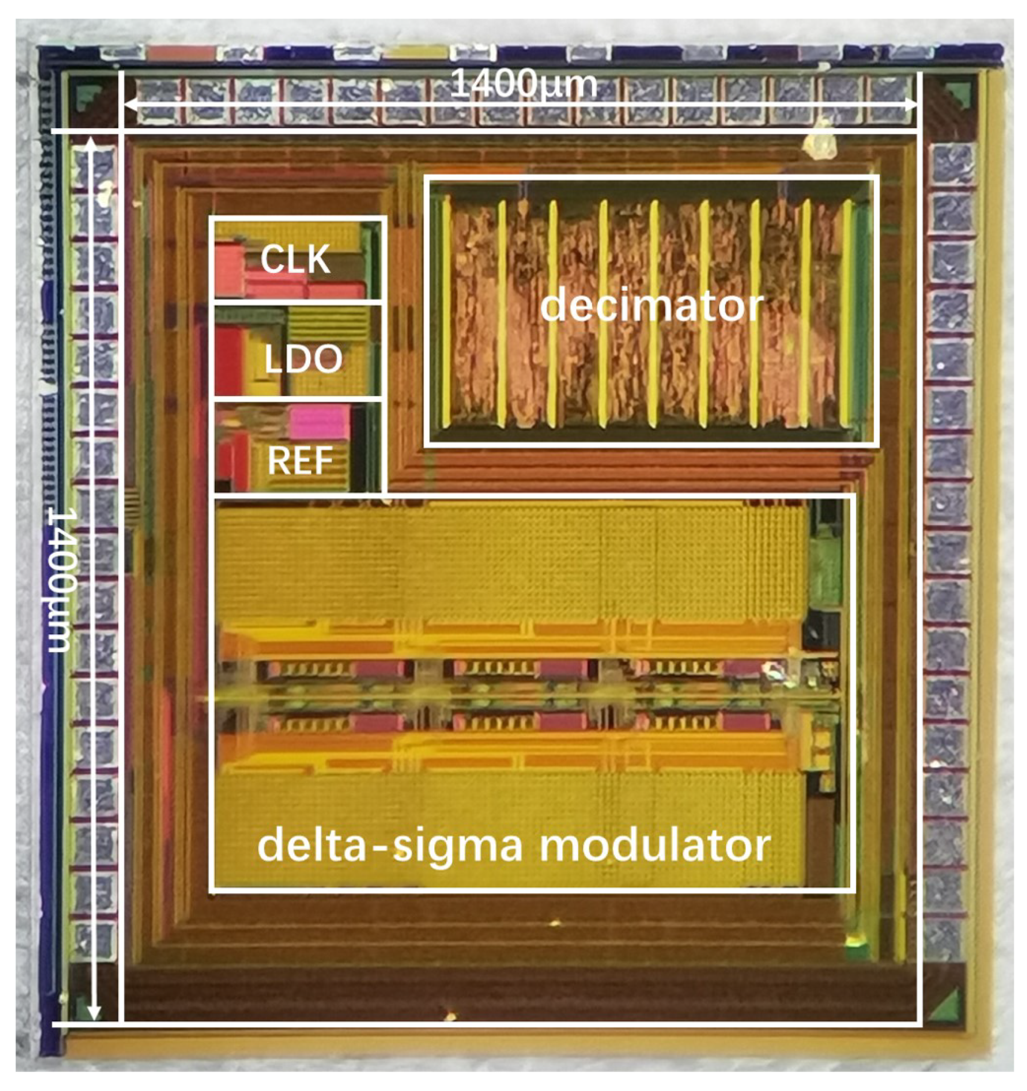
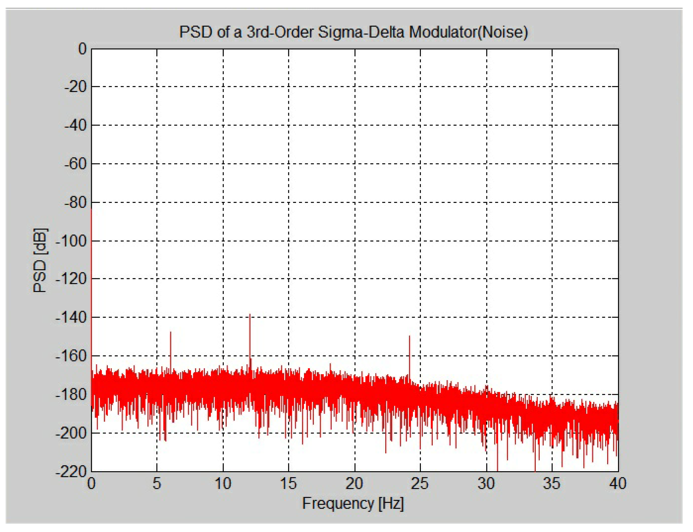
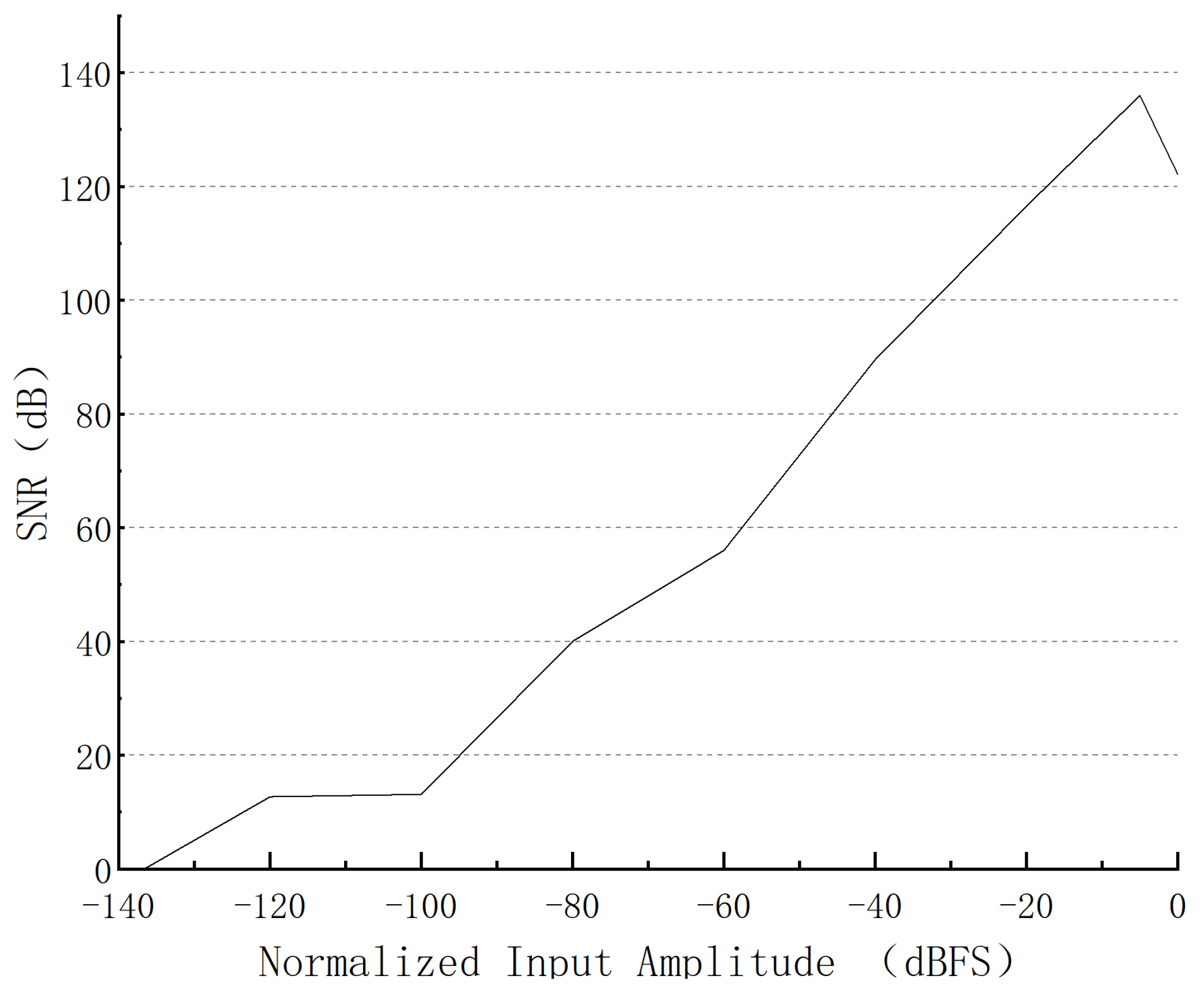
4. Measurement Results
The designed modulator is fabricated in a 0.5 m standard CMOS process. Only regular threshold MOS transistors are adopted in this design. The chip microphotograph is shown in Figure 10. The core chip area is 1.96 mm. The modulator circuit occupies 1.41 mm and the decimator occupies 0.55 mm.
Figure 10.
Chip photograph.
Figure 11 shows the measured output spectrum with 16 Hz input after decimation; the number of samples used for the PSD plot is 16,384. Figure 12 shows the noise floor of the proposed modulator. With the full-scale input of 5 Vpp, the measured ENOB is 22.3 bit. Figure 13 shows the measured SNR versus the input signal amplitudes normalized by reference voltage. The peak SNR reaches 136 dB, and the dynamic range is 137 dB in a 100 Hz signal bandwidth. The modulator consumes 700 A and the decimator consumes 120 A. Table 2 gives the summary of the measurement results.
Figure 11.
Measured output spectrum with 16 Hz input.
Figure 12.
Noise floor of the proposed modulator.
Figure 13.
Measured SNR versus the input signal amplitudes normalized by reference voltage.
Table 2.
Measurement results.
The performance of our modulator is compared with other published high resolution modulators in Table 3. The common FOM equation [13] is shown below:
where is the dynamic range of the modulator, BW is the signal bandwidth, and P is the power consumption. As we can see in Table 3, our modulator shows the highest FOM and is suitable for application of an EEG acquisition system.
Table 3.
Performance comparation.
5. Conclusions
In this paper, a high resolution delta-sigma modulator for acquiring and digitization of EEG signals is presented. A third-order single-loop modulator architecture with a 1-bit quantizer is adopted. By analysing the thermal noise effects and optimizing the feedback and input coefficients, the proposed modulator can achieve best SNR in a full-scale input range of 0 V to 5 V with almost no increase in total capacitance sizes. Fabricated in 0.5 m CMOS technology and operated at 5 V voltage supply, the proposed modulator can achieve 136 dB peak SNR and 137 dB DR with 100 Hz bandwidth. Combined with the characteristics of EEG signals, the measurement results show that this modulator can be used for the application of the EEG acquisition system.
Author Contributions
Conceptualization, Q.W., F.L. and Z.H.; methodology, Q.W., F.L. and Z.H.; software, Q.W., F.L. and L.F.; validation, Q.W. and F.L.; formal analysis, Q.W. and F.L.; investigation, Q.W.; data curation, Q.W., F.L. and L.F.; writing—original draft preparation, Q.W.; writing—review and editing, Q.W., F.L., Q.L., J.K. and K.C.; visualization, Q.W.; supervision, F.L.; project administration, F.L. All authors have read and agreed to the published version of the manuscript.
Funding
This work was funded by the National Key Research and Development Program of China under grant number 2022YFF1202302, and the Beijing Science and Technology Plan under grant number Z201100004320006.
Data Availability Statement
The data presented in this study are available in article.
Acknowledgments
The authors would like to acknowledge the professors and peers at the Institute of the Microelectronics of the Chinese Academy of Sciences and the University of Chinese Academy of Sciences for knowledge sharing and equipment supporting.
Conflicts of Interest
Author Zongliang Huo was employed by the company Yangtze Memory Technologies Company, Ltd. The remaining authors declare that the research was conducted in the absence of any commercial or financial relationships that could be construed as a potential conflict of interest.
Abbreviations
The following abbreviations are used in this manuscript:
| EEG | Electroencephalography |
| AFE | Analog-front-end |
| CMRR | Common-mode-rejection-ratio |
| EOV | Electrode-offset-voltage |
| SNR | Signal to noise ratio |
| SNDR | Signal to noise and distortion ratio |
| OSR | Oversampling ratio |
| NS | Noise shaping |
| MASH | Multistage noise-shaping |
| DEM | Dynamic element matching |
| GBW | Gain bandwidth |
| DR | Dynamic range |
| CMFB | Common-mode feedback |
| ENOB | Effective number of bits |
| FOM | Figure of merit |
| DT | Discrete time |
| MB | Multi-bit |
| CT | Continuous time |
| SB | Single-bit |
| OTA | Operational transconductance amplifier |
| PSD | Power spectrum density |
References
- Yazıcıoglu, R.; Merken, P.; Puers, R.; Hoof, C. A 200 μW eight-channel acquisition ASIC for ambulatory EEG systems. In Proceedings of the IEEE International Solid-State Circuits Conference, San Francisco, CA, USA, 3–7 February 2008. [Google Scholar]
- Webster, J.G. Medical Instrumentation: Application and Design; John Wiley & Sons: Hoboken, NJ, USA, 2009. [Google Scholar]
- Van Rijn, A.M.; Peper, A.; Grimbergen, C. High-quality recording of bioelectric events. Part 1. Interference reduction, theory and practice. Med. Biol. Eng. Comput. 1990, 28, 389–397. [Google Scholar] [CrossRef]
- Yokus, M.A.; Jur, J.S. Fabric-based wearable dry electrodes for body surface biopotential recording. IEEE Trans. Biomed. Eng. 2015, 63, 423–430. [Google Scholar] [CrossRef] [PubMed]
- Tohidi, M.; Madsen, J.K.; Moradi, F. Low-power high-input-impedance EEG signal acquisition SoC with fully integrated IA and signal-specific ADC for wearable applications. IEEE Trans. Biomed. Circuits Syst. 2019, 13, 1437–1450. [Google Scholar] [CrossRef] [PubMed]
- Yoon, Y.; Duan, Q.; Yeo, J.; Roh, J.; Kim, J.; Kim, D. A delta–sigma modulator for low-power analog front ends in biomedical instrumentation. IEEE Trans. Instrum. Meas. 2016, 65, 1530–1539. [Google Scholar] [CrossRef]
- Lee, I.; Kim, B.; Lee, B.G. A low-power incremental delta–sigma ADC for CMOS image sensors. IEEE Trans. Circuits Syst. II Express Briefs 2015, 63, 371–375. [Google Scholar] [CrossRef]
- Nikas, A.; Jambunathan, S.; Klein, L.; Voelker, M.; Ortmanns, M. A continuous-time delta-sigma modulator using a modified instrumentation amplifier and current reuse DAC for neural recording. IEEE J. Solid-State Circuits 2019, 54, 2879–2891. [Google Scholar] [CrossRef]
- Boni, A.; Giuffredi, L.; Pietrini, G.; Ronchi, M.; Caselli, M. A low-power sigma-delta modulator for healthcare and medical diagnostic applications. IEEE Trans. Circuits Syst. I Regul. Pap. 2021, 69, 207–219. [Google Scholar] [CrossRef]
- Edward, A.; Liu, Q.; Briseno-Vidrios, C.; Kinyua, M.; Soenen, E.G.; Karşılayan, A.I.; Silva-Martinez, J. A 43-mW MASH 2-2 CT ΔΣ Modulator Attaining 74.4/75.8/76.8 dB of SNDR/SNR/DR and 50 MHz of BW in 40-nm CMOS. IEEE J. Solid-State Circuits 2016, 52, 448–459. [Google Scholar] [CrossRef]
- Nowacki, B.; Paulino, N.; Goes, J. 15.3 A 1V 77 dB-DR 72 dB-SNDR 10 MHz-BW 2-1 MASH CT ΔΣM. In Proceedings of the 2016 IEEE International Solid-State Circuits Conference (ISSCC), San Francisco, CA, USA, 31 January–4 February 2016; pp. 274–275. [Google Scholar]
- Chebli, R.; Sawan, M. Fully integrated high-voltage front-end interface for ultrasonic sensing applications. IEEE Trans. Circuits Syst. Regul. Pap. 2007, 54, 179–190. [Google Scholar] [CrossRef]
- Rabii, S.; Wooley, B.A. The Design of Low-Voltage, Low-Power Sigma-Delta Modulators; Springer Science & Business Media: Berlin/Heidelberg, Germany, 2012; Volume 483. [Google Scholar]
- Johansson, J.; Neubauer, H.; Hauer, H. A 16-bit 60 μW multi-bit ΣΔ modulator for portable ECG applications. In Proceedings of the ESSCIRC 2004-29th European Solid-State Circuits Conference (IEEE Cat. No. 03EX705), Estoril, Portugal, 16–18 September 2003; pp. 161–164. [Google Scholar]
- Singh, G.; Wu, R.; Chae, Y.; Makinwa, K.A. A 20bit continuous-time ΣΔ modulator with a Gm-C integrator, 120dB CMRR and 15 ppm INL. In Proceedings of the 2012 Proceedings of the ESSCIRC (ESSCIRC), Bordeaux, France, 17–21 September 2012; pp. 385–388. [Google Scholar]
- Xu, L.; Gönen, B.; Fan, Q.; Huijsing, J.H.; Makinwa, K.A. 5.2 A 110 dB SNR ADC with ±30 V input common-mode range and 8 μV Offset for current sensing applications. In Proceedings of the 2015 IEEE International Solid-State Circuits Conference-(ISSCC) Digest of Technical Papers, San Francisco, CA, USA, 22–26 February 2015; pp. 1–3. [Google Scholar]
- Liang, J.; Sin, S.W.; Seng-Pan, U.; Maloberti, F.; Martins, R.P.; Jiang, H. A high DR high-input-impedance programmable-gain ECG acquisition interface with non-inverting continuous time sigma-delta modulator. In Proceedings of the 2019 IEEE Asian Solid-State Circuits Conference (A-SSCC), Macau, China, 4–6 November 2019; pp. 309–312. [Google Scholar]
Disclaimer/Publisher’s Note: The statements, opinions and data contained in all publications are solely those of the individual author(s) and contributor(s) and not of MDPI and/or the editor(s). MDPI and/or the editor(s) disclaim responsibility for any injury to people or property resulting from any ideas, methods, instructions or products referred to in the content. |
© 2023 by the authors. Licensee MDPI, Basel, Switzerland. This article is an open access article distributed under the terms and conditions of the Creative Commons Attribution (CC BY) license (https://creativecommons.org/licenses/by/4.0/).