Article

On the Application of Thévenin Equivalent Circuits to the Analysis of Vacuum Tube Circuits

School of Electrical and Computer Engineering, Georgia Institute of Technology, 777 Atlantic Drive, Atlanta, GA 30332, USA
Electronics 2023, 12(23), 4804; https://doi.org/10.3390/electronics12234804
Submission received: 12 November 2023 / Revised: 25 November 2023 / Accepted: 26 November 2023 / Published: 27 November 2023
(This article belongs to the Section Circuit and Signal Processing)

Abstract

:
In this paper, we express Thévenin equivalent circuits seen looking into the terminals of the small-signal model of the vacuum tube triode in terms of the Thévenin equivalent circuits seen looking out of the other terminals and apply them to the analysis of the common-cathode, common-plate, and common-grid single-tube amplifier configurations, as well as a differential pair amplifier. This is an adaptation of equivalent circuit techniques for transistor circuits pioneered by Marshall Leach. The use of equivalent circuits can yield intuitive solutions that avoid solving sets of equations.

1. Introduction

Although vacuum tubes gave way to transistors during the 1960s and 1970s, they retain a niche status in audio applications [1,2,3,4,5,6,7,8], where they are particularly favored by electric guitarists [9,10,11,12,13,14,15,16,17,18,19] and audiophiles [20,21,22,23,24].
The creation of Thévenin and Norton equivalent circuits is a powerful technique, finding applications in electronics [25] and power systems [26,27,28,29,30,31], particularly battery modeling [32,33,34].
In 1996, Marshall Leach, a professor at the Georgia Institute of Technology, published a paper [35] titled “On the Application of Thévenin and Norton Equivalent Circuits and Signal Flow Graphs to the Analysis of Active Circuits”. In that work, he formulated a Norton equivalent circuit looking into the collector of a bipolar junction transistor (BJT) in terms of the Thévenin equivalents seen looking out of the base and the emitter, a Thévenin equivalent circuit looking into the emitter of terms of the Thévenin equivalent seen looking out of the base, and a Thévenin equivalent circuit looking into the base in terms of the Thévenin equivalent seen looking out of the emitter. Similarly, he formulated a Norton equivalent circuit looking into the drain of a field-effect transistor (FET) in terms of the Thévenin equivalents seen looking out of the gate and the source and a Thévenin equivalent looking into the source in terms of the Thévenin equivalent seen looking out of the gate.
Until he passed away in November 2010, Prof. Leach taught ECE3050: Analog Electronics at Georgia Tech using these equivalent circuits, along with extensive use of superposition with dependent sources. (To this day, most introductory circuits textbooks incorrectly insist that dependent sources may not be “deactivated” when using superposition. The key is to include all contributions before solving for the controlling variable. Numerous examples are provided in [36]; see [37] for technical details. The technique appears to have been independently discovered by Davis [38], who refers to it using the terminology of “taping” and “untaping”.) Prof. Leach introduced the hybrid-pi (see pp. 799–805 and pp. 819–821 of [39] or pp. 385–387 and pp. 405–406 of [40]) and T (see p. 849 of [39] or pp. 393–394 and pp. 405–406 of [40]) small-signal models for BJTs and FETs but stuck with them only long enough to derive his Thévenin and Norton equivalent circuits, which he used throughout the semester to derive the typical results of a junior analog electronics course, without making explicit reference to the underlying small-signal models. Reading a typical electronics textbook, different patterns repeatedly emerge that the equivalent circuits abstract in the way a computer programmer may notice certain repeated patterns in their code and abstract those using a subroutine. He also employed these techniques while teaching the graduate class ECE6416: Low-Noise Electronic Design (see Section 7.7 of [41]). Websites for Marshall Leach’s classes, including ECE3050 and ECE6416, are archived at https://leachlegacy.ece.gatech.edu (last accessed on 25 November 2023).
In 2017, the author taught the first offering of a special-topics class titled “Guitar Amplification and Effects”, which largely focused on vacuum tube circuits, in which he made repeated use of the classic voltage-controlled voltage source (VCVS) small-signal model for a triode. The author discovered Prof. Leach’s approach to teaching electronics in 2018 when he first taught the junior Analog Electronics course and found it to be particularly elegant, allowing some results to flow naturally, almost “by inspection”. Therefore, in 2019, during the second offering of “Guitar Amplification and Effects”, he adapted Prof. Leach’s equivalent-circuit-based techniques to vacuum tubes. This paper presents the resulting equivalent circuits, which have not appeared before in the literature, and some of their applications. It also partially serves as an introduction to vacuum tube circuits for practitioners already accustomed to transistors. Much wisdom about tubes is found in texts [42,43,44] that are over seven decades old; the way schematics are drawn, the terminology used, and even the conceptualization of circuits in these works can seem quite alien to a modern electrical engineer.

2. Thévenin Equivalent Circuits

The leftmost circuit in Figure 1 represents a triode in a generic small-signal circuit. Small-signal quantities v t g and v t k represent the Thévenin voltages seen looking out of the grid and cathode, respectively. R t p and R t k represent the Thévenin resistances seen looking out of the plate and cathode, respectively. Under normal operation, no current flows through the grid, so our analysis does not require knowledge of the resistance seen looking out of the grid, so it is omitted from the diagram, but one could add R t g to the diagram if desired. We use lowercase letters to represent dynamic resistances arising from small-signal models. The use of upper case for R t p and R t k assumes fixed resistances; in the case of a more complex circuit, these may also be dynamic quantities, in which case symbols like r t p and/or r t k might be more appropriate.
The arrow in Figure 1 indicates the expansion of the triode into its small-signal model, which consists of a voltage-controlled voltage source (VCVS) with an intrinsic amplification factor ( μ ) in series with the dynamic plate resistance ( r p ). This is analogous to the hybrid-pi model for transistors. Note that the negative terminal of the VCVS is on top. The voltage of the VCVS is μ v g k , where v g k is the difference between the voltage at the gate (which is just v t g ) and the voltage at the cathode, as denoted by v k (where ⊥ indicates the voltage at the cathode with respect to ground), so v g k = v t g v k .
Small-signal parameters μ and r p (pp. 16–23 of [45]) depend on the plate bias current, which is typically derived from a load-line analysis (see pp. 55–60 of [46], pp. 7–9 of [47], pp. 33–37 of [48], and pp. 191–195 of [49] for examples). Although r p notably varies with bias current, μ is usually constant over a wide range of currents. Compared with parameters such as the transconductance of a transistor, which can vary wildly under different operating conditions and between different specimens of the same transistor model, μ is a parameter a designer can rely upon.
For convenience, we define r t o p = R t p + r p , and for consistency, we define r b o t = R K , as shown in the rightmost diagram in Figure 1. We find it illuminating to consider a Thévenin equivalent circuit found looking into the negative terminal of the VCVS and not the top of r p ; hence, although we find equivalent circuits looking into the cathode, we do not strictly find equivalent circuits looking into the plate. We imagine that we can access an “inner plate” between r p and the VCVS; this shortens the description of the Thévenin equivalent, but one needs to remember to add r p .

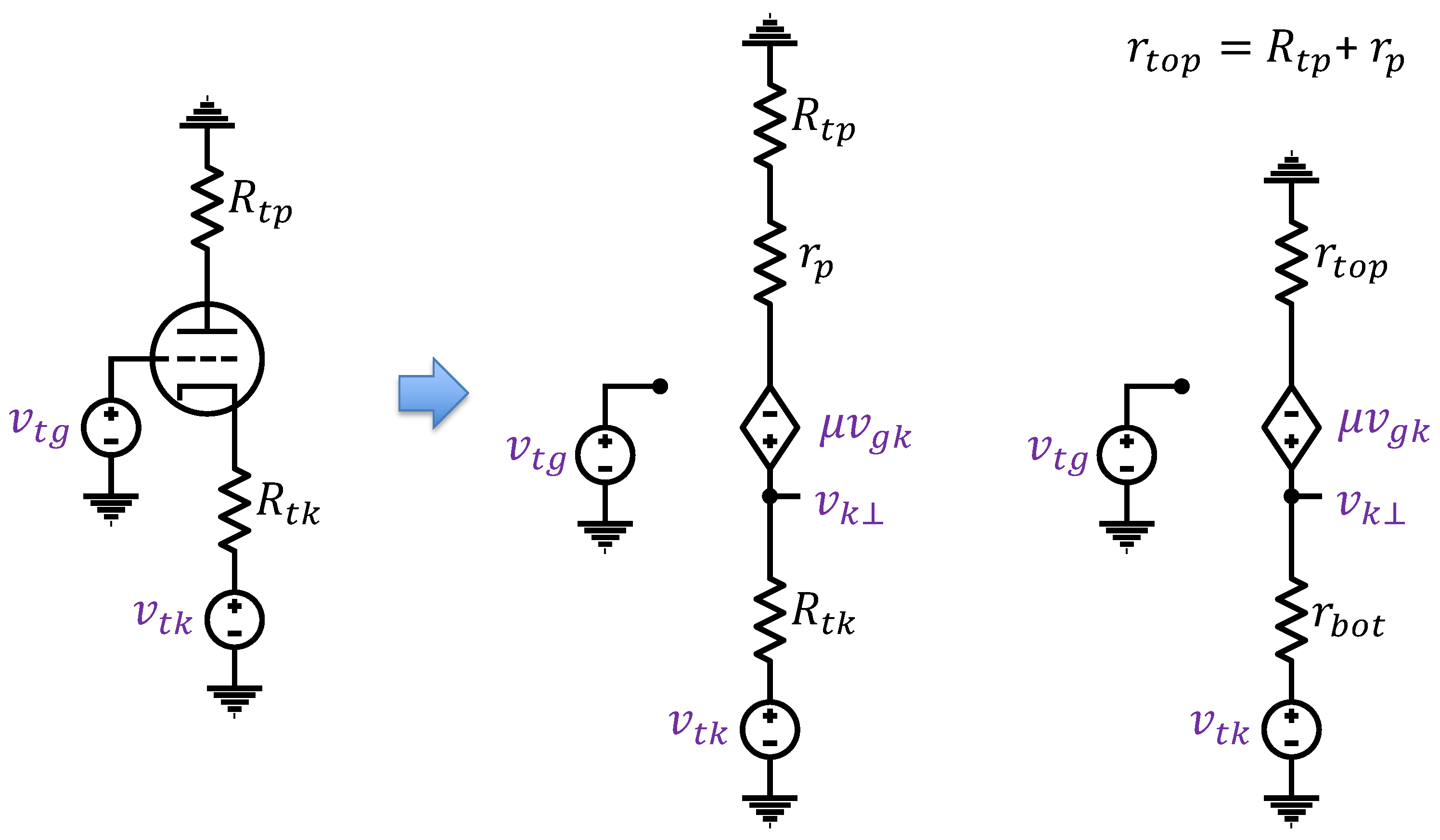
2.1. Looking into the “Inner Plate”

Given v d o w n , the Thévenin voltage seen looking down into the negative terminal of the VCVS in Figure 2 is an open-circuit voltage; no current flows through the circuit, and therefore, no voltage is lost over r b o t . Thus,
v d o w n = v t k μ ( v t g v t k ) = ( μ + 1 ) v t k μ v t g .
To compute the equivalent resistance seen looking down into the negative terminal of the VCVS, we zero the independent sources ( v t g and v t k ); introduce an independent test current source ( i t e s t ), as shown in Figure 3; and compute the resulting v t e s t . Since v k = i t e s t r b o t ,
v t e s t = v k μ ( v k ) = ( μ + 1 ) v k = ( μ + 1 ) i t e s t r b o t .
Hence, the equivalent resistance is
r d o w n = v t e s t i t e s t = ( μ + 1 ) r b o t .
Figure 4 summarizes the resulting Thévenin equivalent circuit.

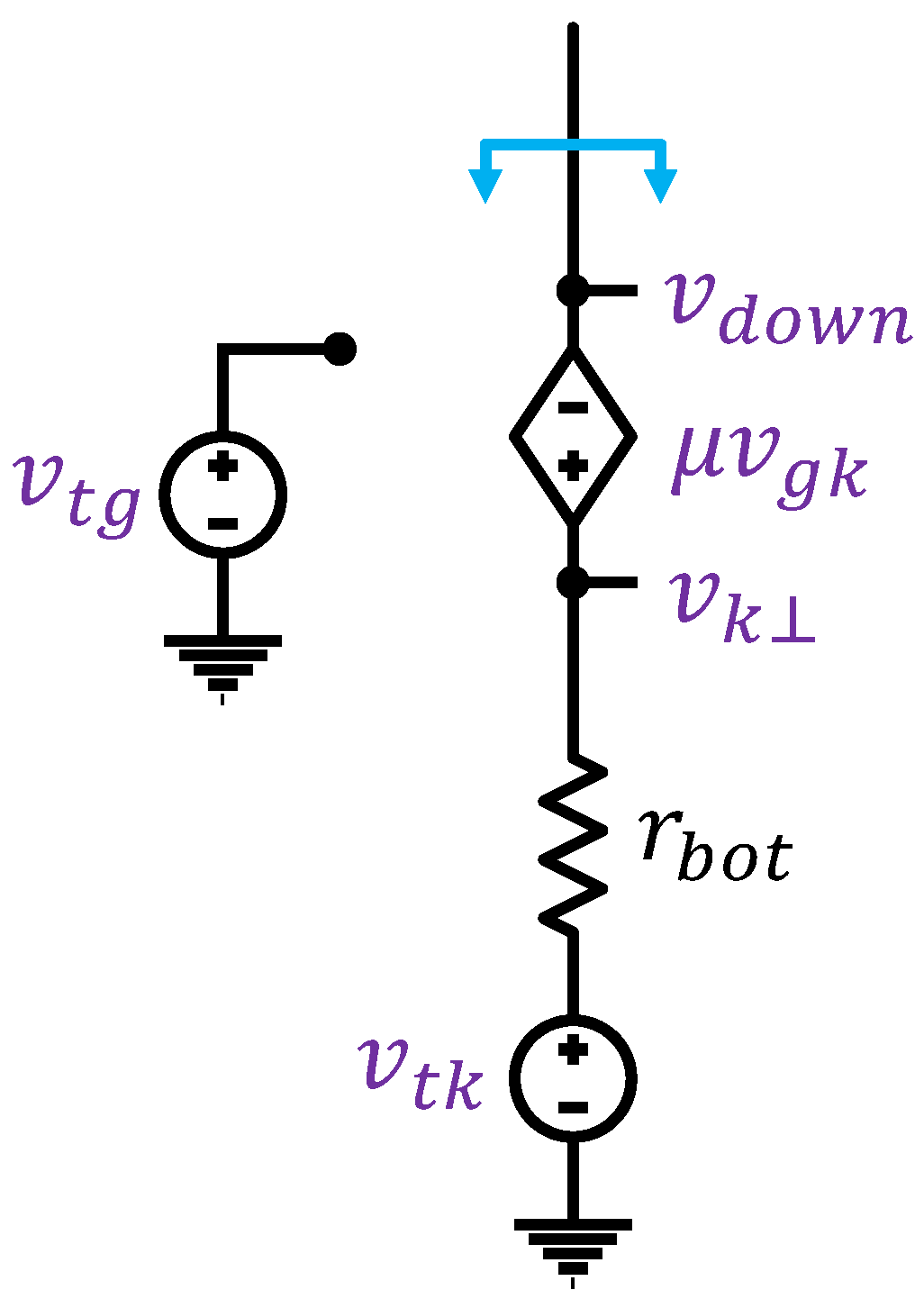
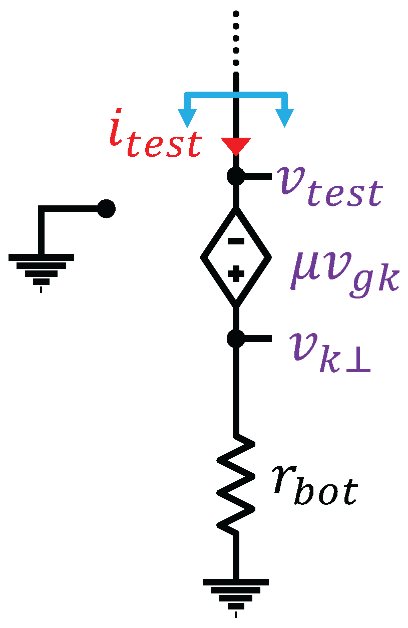
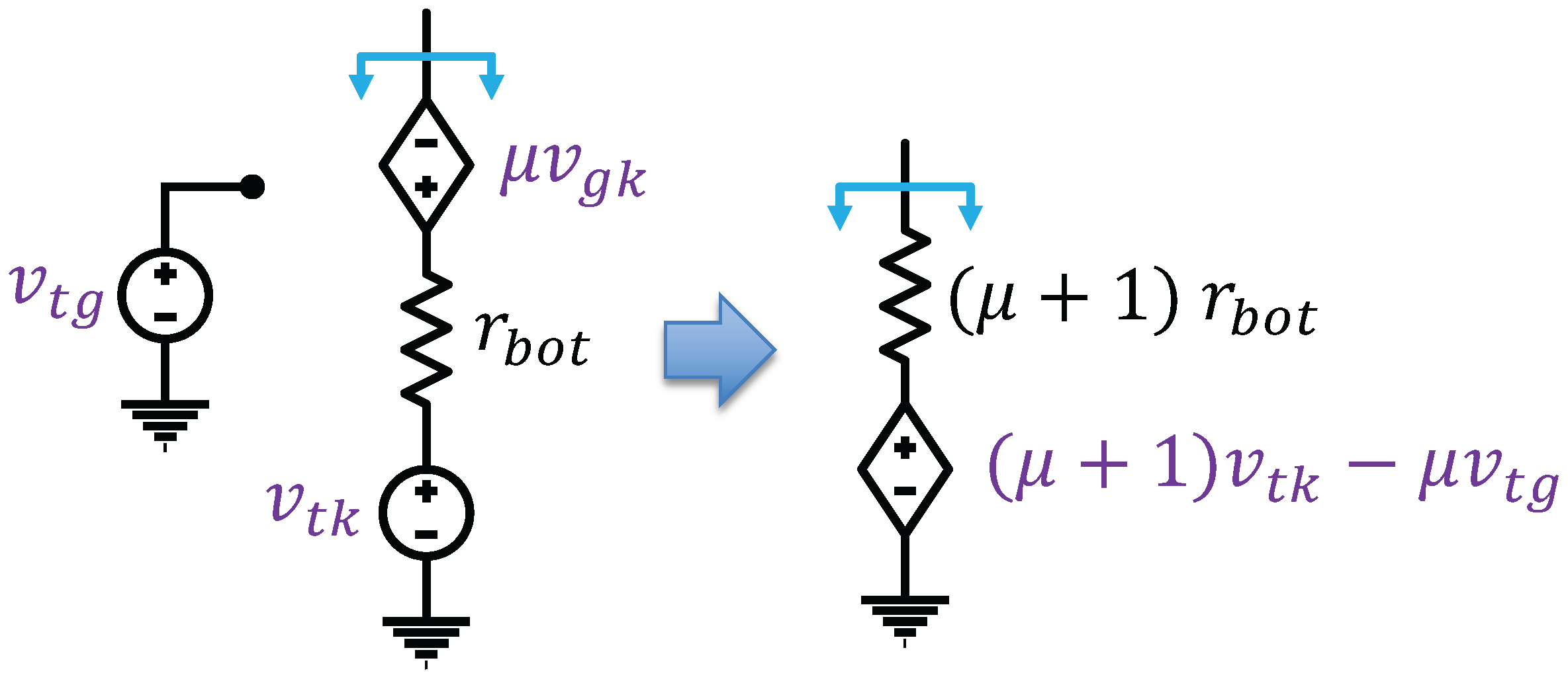
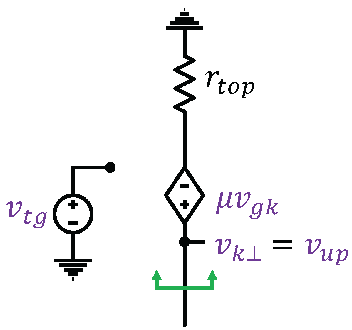
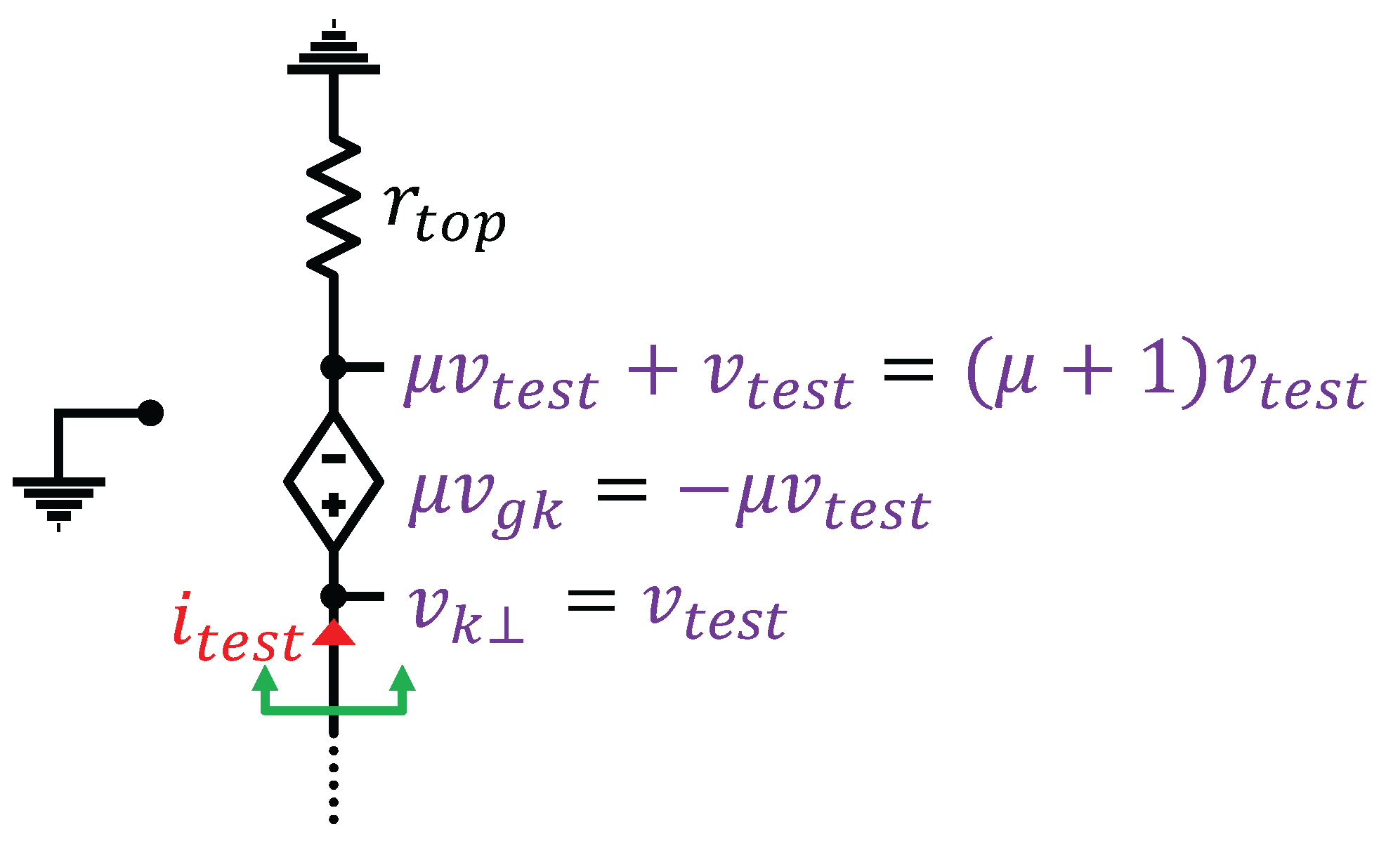
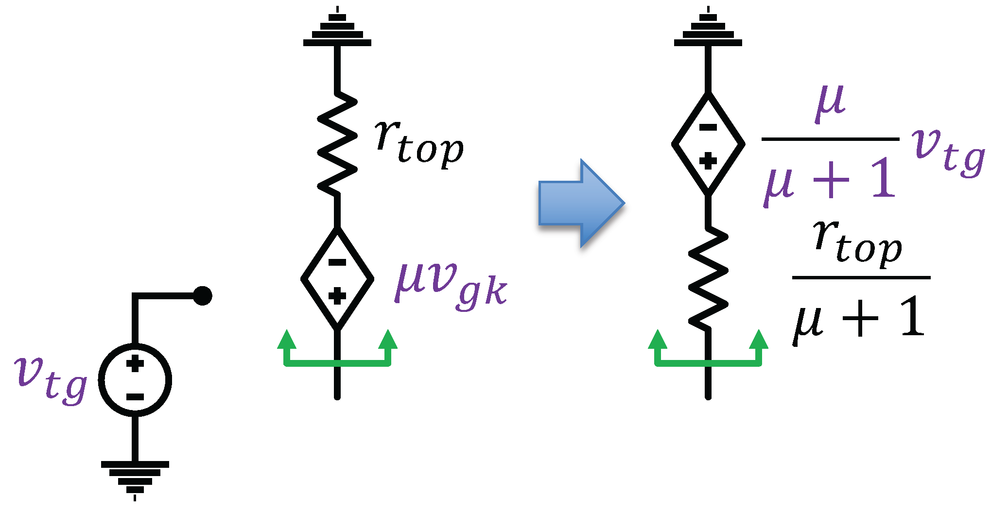
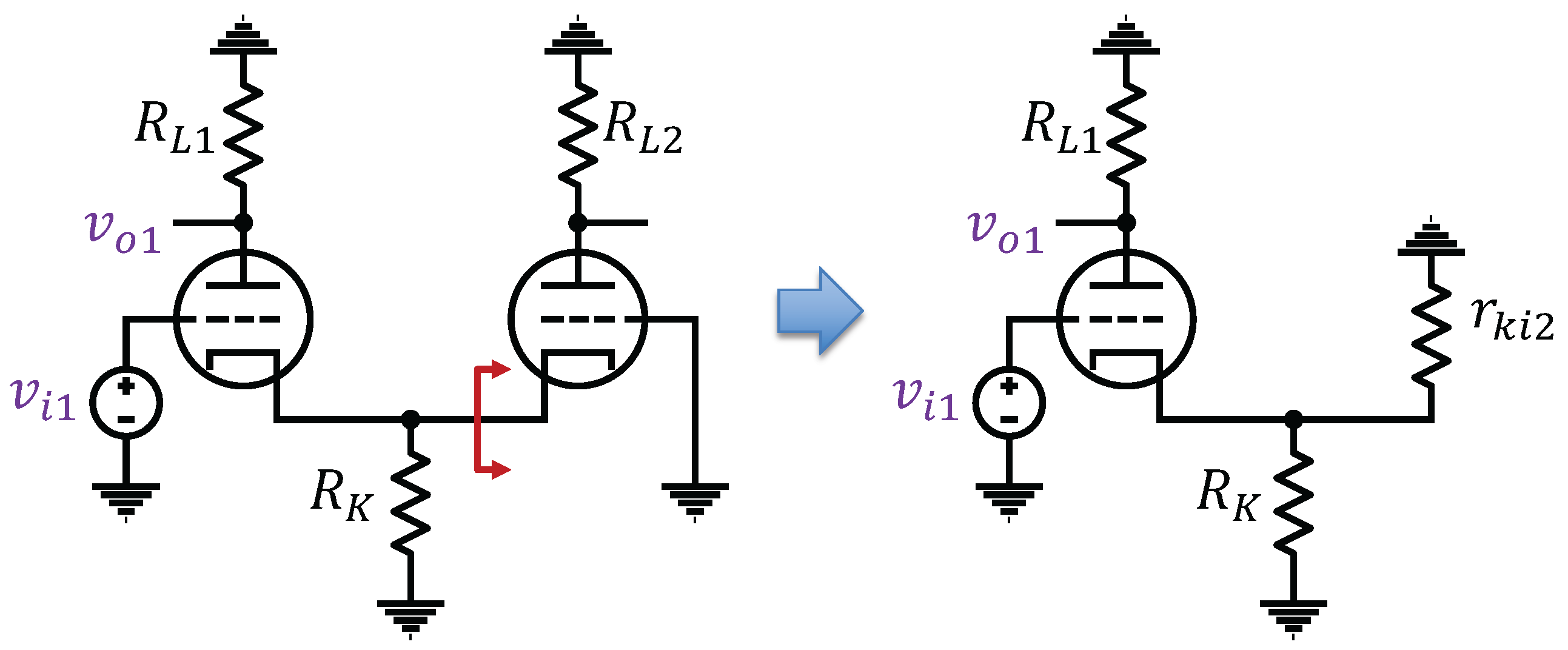
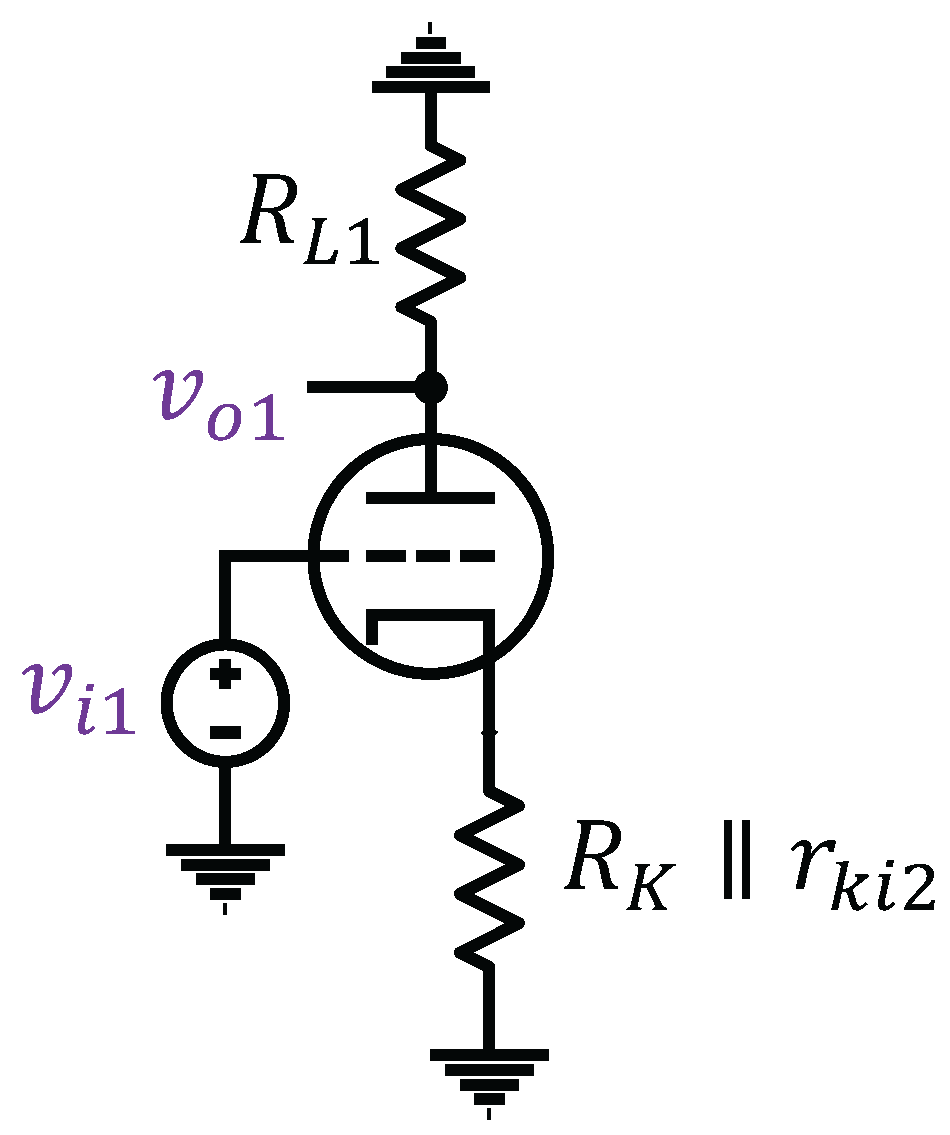
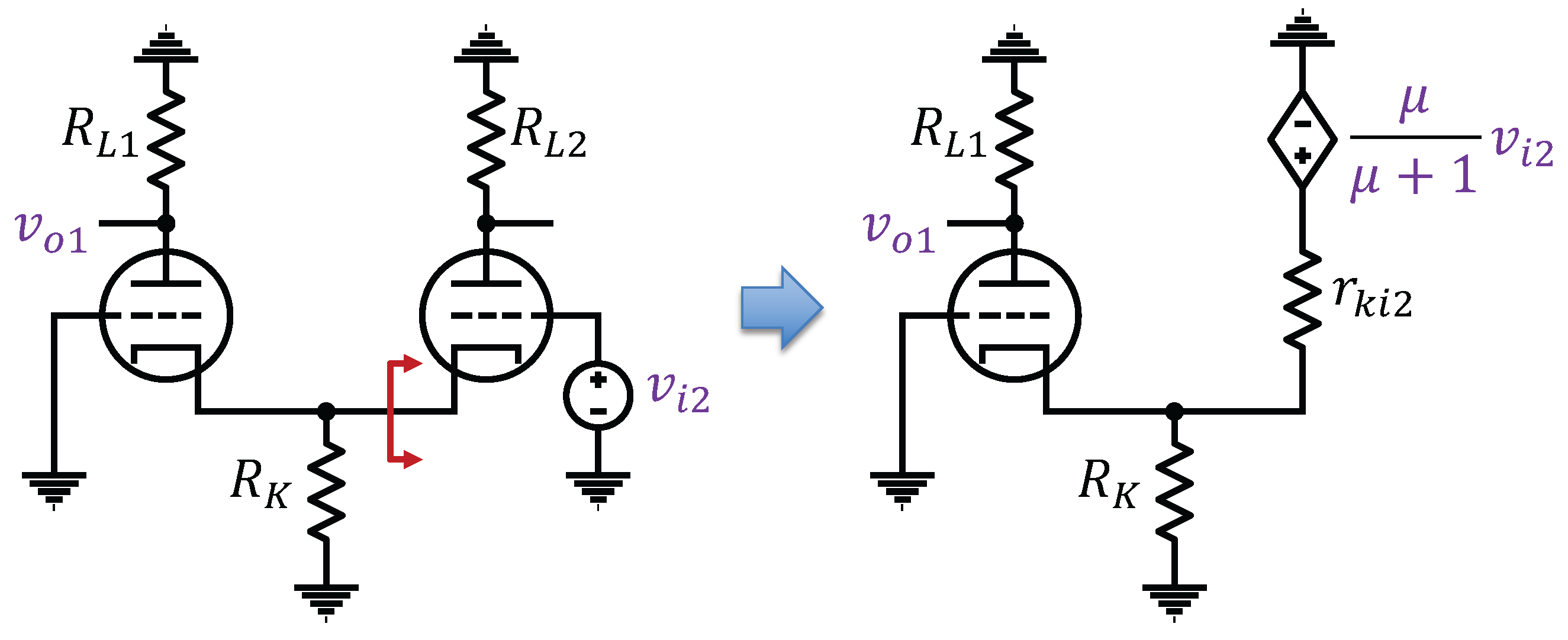
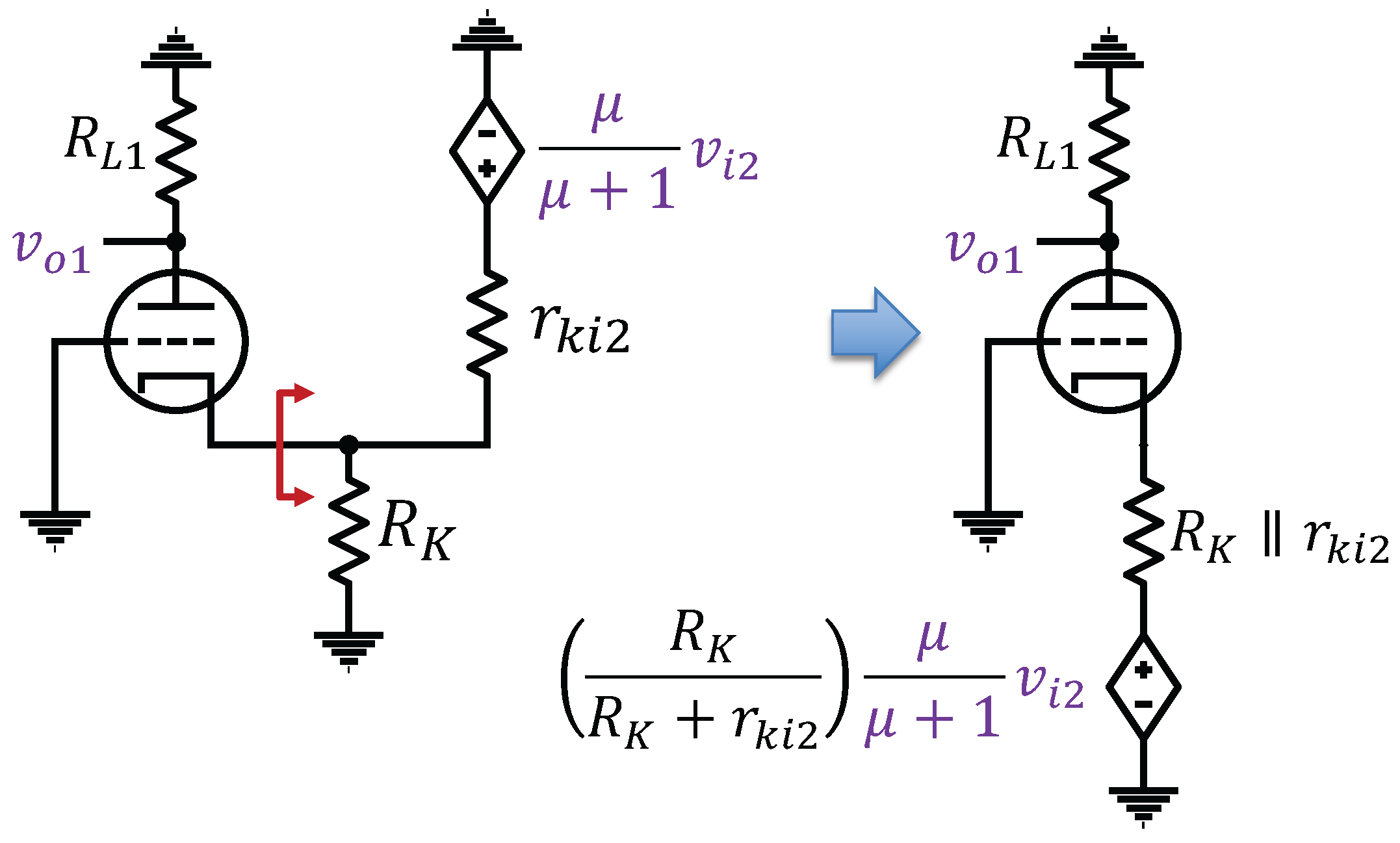
2.2. Looking into the Cathode

Since v u p , the Thévenin voltage seen looking up into the positive terminal of the VCVS in Figure 5 is an open-circuit voltage; no current flows through the circuit, and therefore, no voltage is lost over r t o p . Thus,
v u p = μ ( v t g v u p ) ,
v u p = μ μ + 1 v t g .
To compute the equivalent resistance seen looking up into the positive terminal of the VCVS, we zero the independent source ( v t g ); introduce an independent test voltage source ( v t e s t ), as shown in Figure 6; and compute the resulting i t e s t . Since μ v g k = μ v t e s t , we can compute the voltage at the negative terminal of the VCVS as μ v t e s t + v t e s t = ( μ + 1 ) v t e s t . Hence,
i t e s t = ( μ + 1 ) v t e s t r t o p .
The equivalent resistance is
r u p = v t e s t i t e s t = r t o p μ + 1 .
Figure 7 summarizes the resulting Thévenin equivalent circuit.

3. Applications

Throughout this section, small-signal circuit quantities are represented using lowercase variables with lowercase subscripts, DC bias quantities are represented using uppercase variables with uppercase subscripts, and total quantities are represented using lowercase variables with uppercase subscripts, such as v O U T = V O U T + v o u t .
In this paper, capacitors are assumed to act as short circuits at audio frequencies. The methods described here can be extended to frequency analyses using the methods of short-circuit and open-circuit time constants.

3.1. Common-Cathode Amplifier

The left diagram in Figure 8 shows a typical self-biased common-cathode amplifier (based on Figure 5.7 of [50]). The input at the grid is ground-referenced via the grid leak resistor ( R G ), so v i n = v I N . R K G denotes a resistor connecting the cathode to ground, and R K C denotes a resistor connecting the cathode to the capacitor ( C K ). We refer to the plate resistor as R L instead of R P to avoid confusion with the notation for the dynamic small-signal plate resistance ( r p ). “L” in this context stands for “load”, but this should be thought of as part of the amplifier and not as representing an external load.
The diagrams to the right of the approximation sign in Figure 8 illustrate decomposition into DC bias (middle) and small-signal (right) circuits, where R K = R K G R K C . At DC, the capacitor is an open circuit, so R K C plays no role in the biasing. In the special case of R K C = 0 , R K G is completely bypassed, and we have no “cathode degeneration” (see pp. 267–290 of [51] for examples).
The left diagram in Figure 9 shows the underlying small-signal model replacing the triode symbol in the right diagram of Figure 8. This forms the basis of the usual analysis of the amplifier, as may be found on pp. 39–41 of [52]. Skipping the small-signal model and applying the Thévenin equivalent in Figure 4 yields the right diagram of Figure 9, which permits a more direct solution via voltage division:
v o u t = v i n μ R L R L + r p + ( μ + 1 ) R K .
Zeroing the input source yields the output impedance:
r o u t = R L [ r p + ( μ + 1 ) R K ] .
In the completely bypassed case, where R K = 0 , we have v o u t = v i n μ R L / ( R L + r p ) and r o u t = R L r p .
Since no current flows through the grid, the input impedance is set by R G , which is typically a large value (in the range of megaohms).

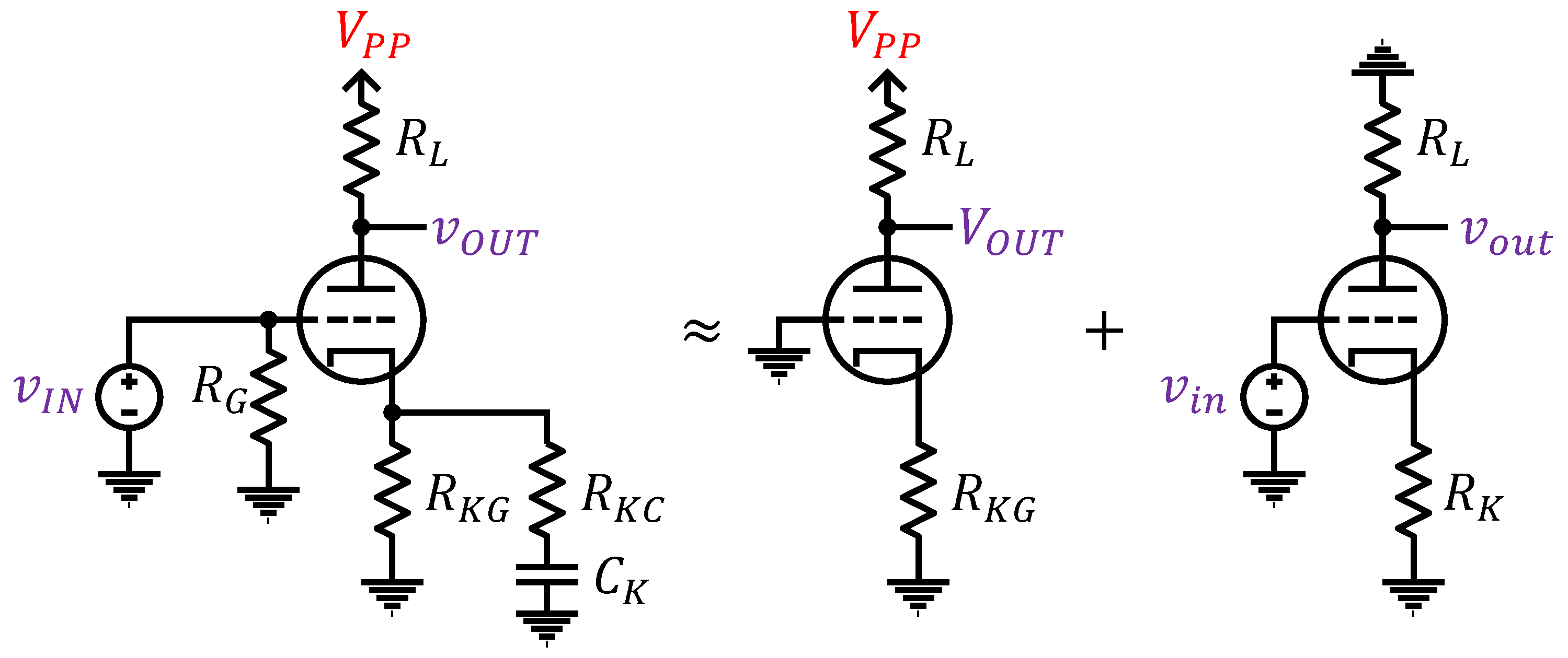
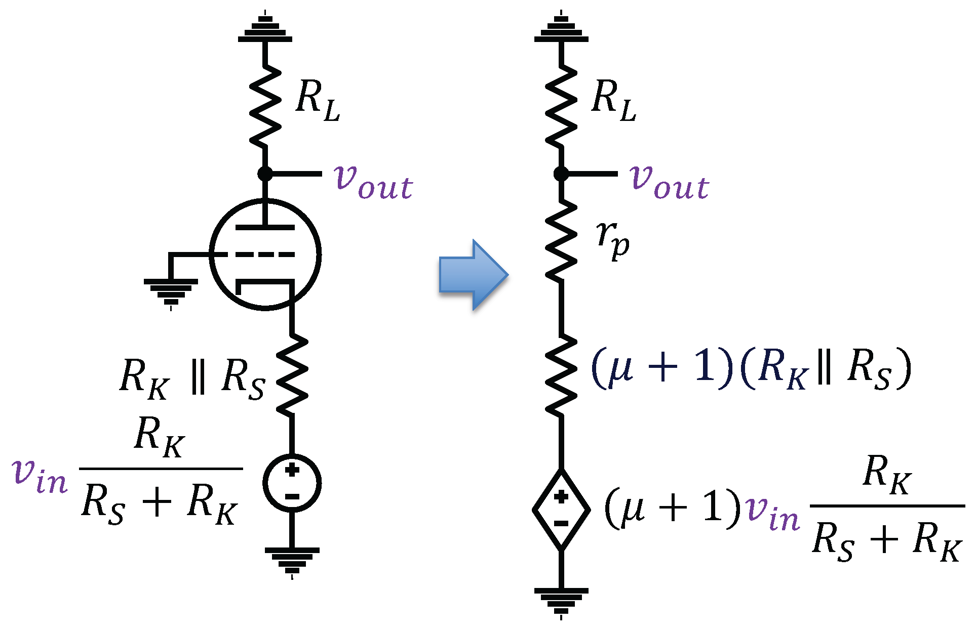
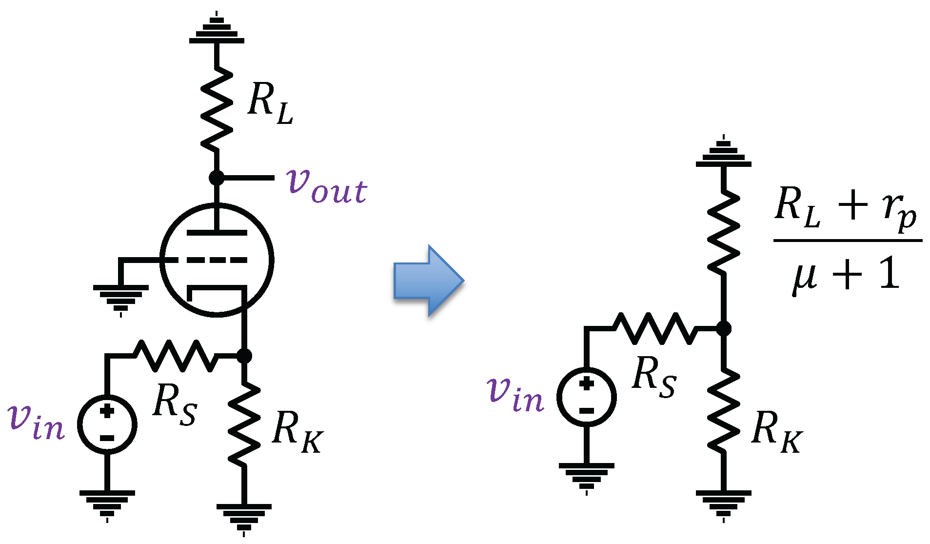
3.2. Common-Plate Amplifier (Cathode Follower)

The left diagram of Figure 10 shows a typical common-plate amplifier, also known as a cathode follower. The flexibility of R K and R T allows for more practical biasing than if the grid leak resistor ( R G ) was hooked to ground, as in the previous example of the common-cathode amplifier. Some practitioners prefer to take the output from the junction of R K and R T (labeled V O U T a l t ) instead of the directly from the cathode (labeled V O U T ). We omitted the DC blocking capacitors typically present at the output.
The two rightmost diagrams of Figure 10 illustrate decomposition into DC bias (middle) and small-signal (right) circuits, assuming that R G is large enough that it can be neglected in the small-signal analysis.
Invoking the Thévenin equivalent circuit in Figure 7 (with r t o p = r p ), we can immediately find the outputs via voltage division:
v o u t = v i n μ μ + 1 · R K + R T R K + R T + r p μ + 1 = v i n μ ( R K + R T ) ( μ + 1 ) ( R K + R T ) + r p ,
v o u t a l t = v i n μ μ + 1 · R T R K + R T + r p μ + 1 = v i n μ R T ( μ + 1 ) ( R K + R T ) + r p .
As μ increases, v o u t approaches v i n , and v o u t a l t approaches v i n R T / ( R K + R T ) , justifying the name “cathode follower.”
Zeroing the input source yields the following output impedances:
r o u t = ( R K + R T ) r p μ + 1 ,
r o u t a l t = R T R K + r p μ + 1 .
Note that the output impedance improves as μ increases.
The input impedance of this particular configuration is even better than that of the common-cathode amplifier due to a “bootstrapping” effect. Since v o u t a l t is only slightly less than v i n , if we reintroduce R G to the small-signal circuit, we see that very little current flows across it relative to an R G hooked between v i n and ground. We do not address this in further detail here; we mention it to contrast with the input impedance of the common-grid amplifier discussed in the next section.

3.3. Common-Grid Amplifier

The left diagram of Figure 11 shows a typical common-grid amplifier (also known as a “grounded grid” amplifier). Such amplifiers have a niche application in high-frequency amplifiers (see pp. 395–397 of [53] and p. 195 of [54]) but are not very common in audio amplifiers; however, they are helpful as building blocks in terms of understanding more complex amplifier structures such as cascodes and differential pair amplifiers, which are addressed in Section 3.4.
In Figure 11, R S represents the output impedance of the source driving the amplifier and is not part of the amplifier itself. We include it here because it appears in the expression for the amplifier’s output impedance, which is not the case for any source impedances for the common-cathode and common-plate configurations.
The two rightmost diagrams of Figure 10 show the amplifier’s decomposition into DC bias (middle) and small-signal (right) circuits. To find the output voltage and output impedance, we want to find the Thévenin equivalent circuit seen looking into the plate; but to find that, we first need the Thévenin equivalent circuit seen looking out of the cathode. As illustrated in Figure 12, the equivalent resistance is just R K in parallel with R S , and the Thévenin voltage is found via a voltage divider, yielding v i n R K / ( R S + R K ) .
We can now find the Thévenin equivalent circuit seen looking into the plate, as visualized in Figure 13. According to Figure 4, the resistance ( r b o t = R K | | R S ) when seen from the other side tube appears as ( μ + 1 ) ( R K | | R S ) , which is in series with the dynamic plate resistance ( r p ). Similarly, the voltage ( v i n R K / ( R S + R K ) ) is multiplied by ( μ + 1 ) .
Voltage division yields the output voltage:
v o u t = v i n ( μ + 1 ) R K R S + R K · R L R L + r p + ( μ + 1 ) ( R K R S ) .
Zeroing the input yields the output impedance:
r o u t = R L [ r p + ( μ + 1 ) ( R K R S ) ] .
Finally, we calculate the input impedance seen looking from the right side of R S into the junction of R K and the cathode in the small-signal circuit (right diagram of Figure 11). For this, we need the Thévenin equivalent circuit looking up into the cathode; applying Figure 7 yields the right diagram of Figure 14, from which we find
r i n = R K R L + r p μ + 1 .
This explains why common-grid amplifiers are not as common as common-cathode amplifiers; their input impedance (assuming information is represented as a voltage) is poor in comparison and becomes worse as μ increases.

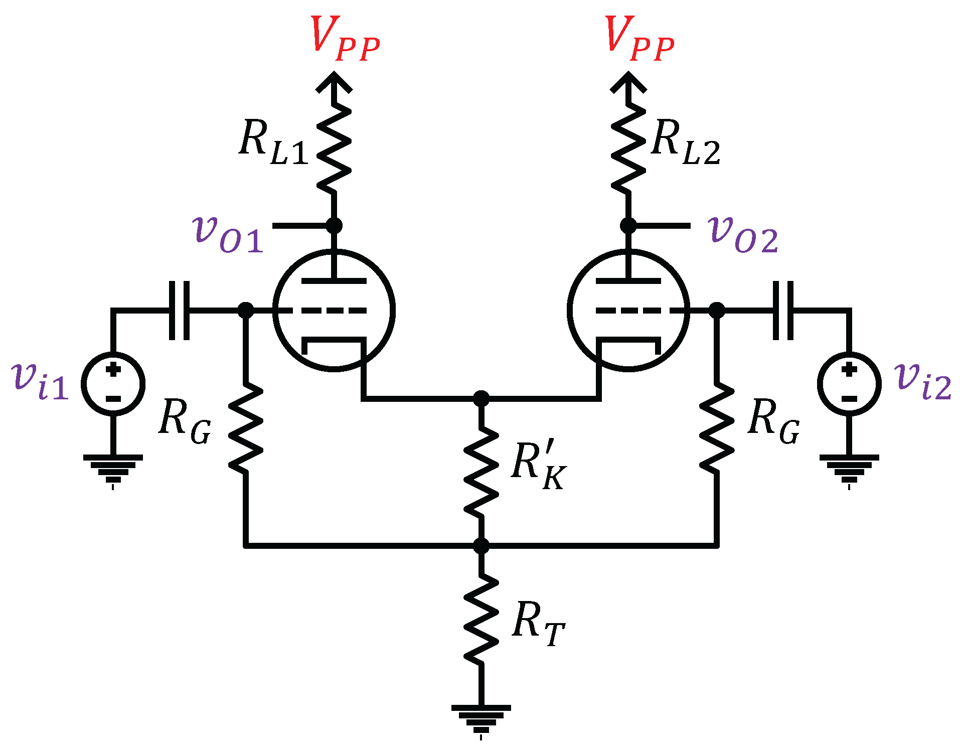
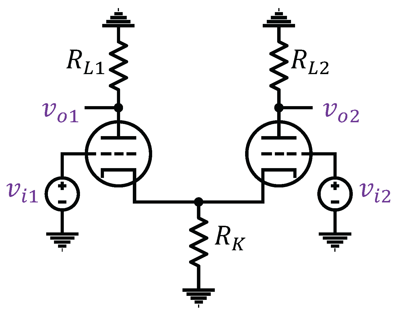
3.4. Differential Amplifier: The Long-Tailed Pair

Transistor-based audio amplifiers often have a push–pull output stage consisting of a complementary pair, such as an NPN and a PNP or an nFET and a pFET. Vacuum tubes are somewhat analogous to NPNs or nFETs; there is no tube equivalent of a PNP or pFET. Hence, building a push–pull stage with vacuum tubes is like having to build a push–pull stage with only NPNs or only nFETs. Hence, a “phase splitter” is needed to create an inverted copy of the original signal [55]. One approach is to simply use an inverting unity-gain common-cathode amplifier while leaving the original signal alone; this is referred to as a “paraphase inverter”. Another approach, referred to as a “cathodyne” or “concertina”, is to add a plate resistor to a cathode follower as in Section 3.2, forming a combination of a cathode follower and a common-cathode amplifier, which provides buffering for the original signal. This can be analyzed by adding a fixed plate load resistance ( R L ) to the dynamic plate resistance ( r p ) in the formulas presented in Section 3.2.
A third approach is to use a differential amplifier such as that shown in in Figure 15, colloquially known as a “long-tailed pair”, which has the advantage of offering gain in addition to providing original and inverted signals. Letting R K = R K + R T , Figure 16 shows the corresponding small-signal circuit, assuming that grid leak resistances ( R G ) are sufficiently large that they can be neglected in the small-signal analysis.
This exposition focuses on v o 1 ; the results for v o 2 can be found by swapping variables. We tackle the circuit via superposition, zeroing v i 2 , and by considering the effect of v i 1 , then by zeroing v i 1 and considering the effect of v i 2 , which is a slightly more complicated situation.
We begin by studying the effect of v i 1 in v o 1 . As illustrated in Figure 17, if we zero v i 2 , we can replace the right tube and R L 2 with r k i 2 , the Thévenin equivalent resistance seen looking into the cathode of the right tube:
r k i 2 = r p + R L 2 μ + 1 .
Combining the parallel resistances ( R K and r k i 2 ), Figure 18 clarifies that we have the form of a common-cathode amplifier. Applying (8) yields
v o 1 = v i 1 μ R L 1 R L 1 + r p + ( μ + 1 ) ( R K r k i 2 ) .
We now zero v i 1 and study the effect of v i 2 on v o 1 . As illustrated in Figure 19, if we zero v i 2 , we can replace the right tube and R L 2 with the Thévenin equivalent circuit looking into the cathode of the right tube according to Figure 7.
We can then find a Thévenin equivalent circuit looking out of the cathode of the left tube, as shown in Figure 20. The Thévenin voltage can be found with a voltage divider, and the Thévenin resistance is just a parallel combination. The circuit now resembles a common-grid amplifier. Employing the Thévenin equivalent of Figure 4 reveals Figure 21, in which the μ + 1 factors in the numerator and the denominator of the multiplier of the VCVS cancel each other out. We can then find v o 1 via voltage division:
v o 1 = v i 2 μ R L 1 R L 1 + r p + ( μ + 1 ) ( R K r k i 2 ) · R K R K + r k i 2 .
Note that (19) resembles (18), with v i 2 replacing v i 1 , multiplied by R K / ( R K + r k i 2 ) .
Using superposition, we combine (18) and (19) to yield
v o 1 = μ R L 1 r p + R L 1 + ( μ + 1 ) ( R K r k i 2 ) v i 1 + v i 2 R K R K + r k i 2 .
Some designers let R L 1 = R L 2 , as seems natural; others set them to have different values in an attempt to compensate for the effect of the R K / ( R K + r k i 2 ) factor.
Zeroing v i 2 in Figure 21 yields the following output impedance:
r o 1 = R L 1 [ r p + ( μ + 1 ) ( R K r k i 2 ) ] .
The equivalent formulas for the second output can be derived from (17), (20), and (21) by swapping symbols:
r k i 1 = r p + R L 1 μ + 1 ,
v o 2 = μ R L 2 r p + R L 2 + ( μ + 1 ) ( R K r k i 1 ) v i 2 + v i 1 R K R K + r k i 1 ,
r o 2 = R L 2 [ r p + ( μ + 1 ) ( R K r k i 1 ) ] .
For clarity, we assume that μ and r p are the same for both tubes; one could study the effect of mismatched tubes by repeating the analysis with “1” and “2” subscripts on the small-signal parameters.
The direct derivation given above can be contrasted with the more cumbersome exposition on pp. 96–99 of [52], which involves solving a set of simultaneous equations.

4. Conclusions and Directions for Future Work

This paper presents Thévenin equivalent circuits looking into the positive and negative terminals of the VCVS of the small-signal triode model. The former corresponds to looking into the cathode, and the latter can be interpreted as looking into the plate side of the tube but bypassing the dynamic plate resistance ( r p ), which can be readily added back in. We applied these equivalent circuits to the three standard single-tube amplifier configurations and a differential pair amplifier. The equivalent circuits let us intuitively derive gains, as well as input and output impedances, without having to solve systems of node-voltage or mesh-current equations. This approach can be applied to other structures, such as cascodes.
The title of Leach’s paper [35], which inspired this one, contained the words “and Signal Flow Graphs”, which are missing from the title of this paper. Leach used Mason flow graphs [56] to analyze transistor feedback amplifiers. Although some guitar amplifiers use feedback from the speaker side of the output transformer of their power amplifier to help linearize the response, it is rare to find guitar amplifiers that use feedback in preamplifier stages, so we did not considered this case here. We conjecture that this is because the parameters of tubes are generally more consistent than those of transistors; in transistor circuits, feedback is a useful way of handling transistor variation. Future work could explore the analysis of feedback amplifiers using our Thévenin equivalent circuits combined with Mason flow graph techniques.
The analysis reported in this paper could be characterized as “midband”, since it assumes that capacitors can be approximated as short circuits for small signals. The Thévenin equivalent circuits presented in this paper could be readily extended from resistances to generic impedances and used to determine the effect of component capacitors and parasitic capacitances on the bass and treble responses.
This paper is dedicated in loving memory of Marshall Leach, who was always generous with his time and knowledge and was extremely patient with the author and his many questions.

Funding

This research received no external funding.

Data Availability Statement

No new data were created or analyzed in this study. Data sharing is not applicable to this article.

Conflicts of Interest

The author declares no conflict of interest.

Abbreviations

The following abbreviations are used in this manuscript:
BJTBipolar junction transistor
FETField-effect transistor
VCVSVoltage-controlled voltage source

References

  1. Hamm, R. Tubes Versus Transistors-Is There an Audible Difference. J. Audio Eng. Soc. 1973, 21, 267–273. [Google Scholar]
  2. Leach, W. SPICE Models for Vacuum-Tube Amplifiers. J. Audio Eng. Soc. 1995, 43, 117–126. [Google Scholar]
  3. Sjursen, W. Improved SPICE Model for Triode Vacuum Tubes. J. Audio Eng. Soc. 1997, 45, 1082–1088. [Google Scholar]
  4. Kashuba, A. Ab Initio Model for Triode Tube. J. Audio Eng. Soc. 1999, 47, 373–377. [Google Scholar]
  5. Tsambos, P. Three-Halves-Power Law Models for Actual Vacuum Tubes. J. Audio Eng. Soc. 2020, 68, 441–453. [Google Scholar] [CrossRef]
  6. Oshimo, S.; Hamasaki, T. Physically Based Unified Modeling for a Series of Miniature Twin Triode Tubes. J. Audio Eng. Soc. 2018, 66, 808–822. [Google Scholar] [CrossRef]
  7. Abuelma’atti, M. Large-Signal Analysis of Triode Vacuum-Tube Amplifiers. J. Audio Eng. Soc. 2003, 51, 1046–1053. [Google Scholar]
  8. Orcioni, S.; Terenzi, A.; Cecchi, S.; Piazza, F.; Carini, A. Identification of Volterra Models of Tube Audio Devices using Multiple-Variance Method. J. Audio Eng. Soc. 2018, 66, 823–838. [Google Scholar] [CrossRef]
  9. Pittman, A. The Tube Amp Book, Deluxe Revised ed.; Backbeat: London, UK, 2003. [Google Scholar]
  10. Hunter, D. The Guitar Amp Handbook: Understanding Tube Amplifiers and Getting Great Songs; Backbeat: London, UK, 2005. [Google Scholar]
  11. Hunter, D. Guitar Rigs: Classic Guitar and Amp Combinations; Backbeat: London, UK, 2005. [Google Scholar]
  12. Barbour, E. The Cool Sound of Tubes. IEEE Spectr. 1998, 35, 24–35. [Google Scholar] [CrossRef]
  13. Pakarinen, J.; Yeh, D. A Review of Digital Techniques for Modeling Vacuum-Tube Guitar Amplifiers. Comput. Music J. 2009, 33, 85–100. [Google Scholar] [CrossRef]
  14. Neumann, U.; Irving, M. Guitar Amplifier Overdrive: A Visual Tour; Lulu: Raleigh, NC, USA, 2015. [Google Scholar]
  15. Kuehnel, R. Guitar Amplifier Electronics: System Design; Amp Books: Seattle, WA, USA, 2019. [Google Scholar]
  16. Kuehnel, R. Guitar Amplifier Electronics: Circuit Simulation; Amp Books: Seattle, WA, USA, 2019. [Google Scholar]
  17. Kuehnel, R. Guitar Amplifier Electronics: Fender Bassman; Amp Books: Seattle, WA, USA, 2021. [Google Scholar]
  18. Kuehnel, R. Guitar Amplifier Electronics: Fender Deluxe; Amp Books: Seattle, WA, USA, 2021. [Google Scholar]
  19. Kuehnel, R. Guitar Amplifier Electronics: Soldano SLO; Amp Books: Seattle, WA, USA, 2021. [Google Scholar]
  20. Hood, J. Valve and Transistor Audio Amplifiers; Newnes: Oxford, UK, 1997. [Google Scholar]
  21. Jones, M. Valve Amplifiers, 3rd ed.; Newnes: Oxford, UK, 2003. [Google Scholar]
  22. Jones, M. Building Valve Amplifiers; Newnes: Oxford, UK, 2004. [Google Scholar]
  23. Rozenblit, B. Tubes and Circuits; Transcendent Sound: Kansas City, MO, USA, 2012. [Google Scholar]
  24. Circuits for Audio Amplifiers; Segment: Vernon, CT, USA, 1959.
  25. Tomasin, L.; Bevilacqua, A. A Time-Variant Analysis of Passive Resistive Mixers Using Thévenin Theorem. In Proceedings of the 2023 18th Conference on Ph.D Research in Microelectronics and Electronics (PRIME), Valencia, Spain, 18–21 June 2023. [Google Scholar] [CrossRef]
  26. Zhou, X.; Liu, Y.; Chang, P.; Xue, F.; Zhang, T. Voltage Stability Analysis of a Power System with Wind Power Based on the Thévenin Equivalent Analytical Method. Electronics 2022, 11, 1758. [Google Scholar] [CrossRef]
  27. Donnelly, T.; Pekarek, S.; Fudge, D.; Zarate, N. Thévenin Equivalent Circuits for Modeling Common-Mode Behavior in Power Electronic Systems. IEEE Open Access J. Power Energy 2020, 7, 163–172. [Google Scholar] [CrossRef]
  28. Holder, M. Thévenin’s Theorem and a Black Box. IEEE Trans. Educ. 2009, 52, 573–575. [Google Scholar] [CrossRef]
  29. Su, H.Y.; Liu, T.Y. Robust Thévenin Equivalent Parameter Estimation for Voltage Stability Assessment. IEEE Trans. Power Syst. 2018, 33, 4637–4639. [Google Scholar] [CrossRef]
  30. Sun, T.; Li, Z.; Rong, S.; Lu, J.; Li, W. Effect of Load Change on the Thévenin Equivalent Impedance of Power System. Energies 2017, 10, 330. [Google Scholar] [CrossRef]
  31. Heydt, G. Thévenin’s Theorem Applied to the Analysis of Polyphase Transmission Circuits. IEEE Trans. Power Deliv. 2017, 32, 72–77. [Google Scholar] [CrossRef]
  32. Barletta, G.; DiPrima, P.; Papurello, D. Thévenin’s Battery Model Parameter Estimation Based on Simulink. Energies 2022, 15, 6207. [Google Scholar] [CrossRef]
  33. Salazar, D.; Garcia, M. Estimation and Comparison of SOC in Batteries Used in Electromobility Using the Thévenin Model and Coulomb Ampere Counting. Energies 2022, 15, 7204. [Google Scholar] [CrossRef]
  34. Suti, A.; Di Rito, G.; Mattei, G. Development and Experimental Validation of Novel Thévenin-Based Hysteretic Models for Li-Po Battery Packs Employed in Fixed-Wing UAVs. Energies 2022, 15, 9249. [Google Scholar] [CrossRef]
  35. Leach, W. On the Application of Thévenin and Norton Equivalent Circuits and Signal Flow Graphs to the Small-Signal Analysis of Active Circuits. IEEE Trans. Circuits Syst.—I Fundam. Theory Appl. 1996, 43, 885–893. [Google Scholar] [CrossRef]
  36. Leach, W. On the Application of Superposition to Dependent Sources in Circuit Analysis. Available online: https://leachlegacy.ece.gatech.edu/papers/superpos.pdf (accessed on 25 November 2023).
  37. Damper, R. Can Dependent Sources be Suppressed in Electrical Circuit Theory? Int. J. Electron. 2011, 98, 543–553. [Google Scholar] [CrossRef]
  38. Davis, A. Some Fundamental Topics in Introductory Circuit Analysis: A Critique. IEEE Trans. Educ. 2000, 43, 330–335. [Google Scholar] [CrossRef]
  39. Jaeger, R.; Blalock, T. Microelectronic Circuit Design, 4th ed.; McGraw-Hill Education: New York, NY, USA, 2010. [Google Scholar]
  40. Sedra, A.; Smith, K.; Carusone, T.; Gaudet, V. Microelectronic Circuits, 8th ed.; Oxford University Press: Oxford, UK, 2019. [Google Scholar]
  41. Leach, W. Fundamentals of Low-Noise Electronics, 4th ed.; Kendall Hunt: Dubuque, IA, USA, 2012. [Google Scholar]
  42. Reich, H. Principles of Electron Tubes; McGraw-Hill: New York, NY, USA, 1941. [Google Scholar]
  43. Cruft Electronics Staff. Electronic Circuits and Tubes; McGraw-Hill: New York, NY, USA, 1947. [Google Scholar]
  44. Fischer, B. Radio and Television Mathematics; Macmillan: London, UK, 1949. [Google Scholar]
  45. DeFrance, J. Electronic Tubes and Semiconductors; Prentice-Hall: Hoboken, NJ, USA, 1958. [Google Scholar]
  46. Kuehnel, R. Guitar Amplifier Electronics: Basic Theory; Amp Books: Seattle, WA, USA, 2018. [Google Scholar]
  47. Kuehnel, R. Vacuum Tube Circuit Design: Guitar Amplifier Preamps, 2nd ed.; Amp Books: Seattle, WA, USA, 2009. [Google Scholar]
  48. Hood, J. Design and Construction of Tube Guitar Amplifiers, 3rd ed.; TacTec Press: San Jose, CA, USA, 2012. [Google Scholar]
  49. Brazee, J. Semiconductor and Tube Electronics; Holt, Rinehart and Winston: New York, NY, USA, 1968. [Google Scholar]
  50. Blencowe, M. Designing Tube Preamps for Guitar and Bass; Lulu: Raleigh, NC, USA, 2009. [Google Scholar]
  51. Dailey, D. Electronics for Guitarists, 2nd ed.; Springer: New York, NY, USA, 2013. [Google Scholar]
  52. Kuehnel, R. Circuit Analysis of a Legendary Tube Amplifier: The Fender Bassman 5F6-A, 3rd ed.; Amp Books: Seattle, WA, USA, 2009. [Google Scholar]
  53. Everitt, W. (Ed.) Fundamentals of Radio and Electronics, 2nd ed.; Prentice Hall: Seattle, WA, USA, 1958. [Google Scholar]
  54. Millman, J. Vacuum-Tube and Semiconductor Electronics; McGraw-Hill: New York, NY, USA, 1958. [Google Scholar]
  55. Kuehnel, R. Vacuum Tube Circuit Design: Guitar Amplifier Power Amps, 2nd ed.; Amp Books: Seattle, WA, USA, 2008. [Google Scholar]
  56. Mason, S. Feedback Theory–Further Properties of Signal Flow Graphs. Proc. IRE 1956, 44, 920–926. [Google Scholar] [CrossRef]
Figure 1. Small-signal triode model with Thévenin equivalents seen looking out of the plate, grid, and cathode (left), explicitly expanded into the VCVS ( μ v g k ) in series with the dynamic plate resistance ( r p ) (middle). In the diagram on the right, R t p and r p are combined into r t o p .
Electronics 12 04804 g001
Figure 2. Circuit for the computation of the Thévenin voltage seen looking down into the negative terminal of the VCVS of the small-signal triode model.
Electronics 12 04804 g002
Figure 3. Circuit for computing the equivalent resistance seen looking down into the negative terminal of the VCVS of the small-signal triode model.
Electronics 12 04804 g003
Figure 4. Summary of the Thévenin equivalent circuit seen looking down into the negative terminal of the VCVS of the small-signal triode model. We repeatedly refer to this figure in this paper.
Electronics 12 04804 g004
Figure 5. Circuit for computing the Thévenin voltage seen looking up into the positive terminal of the VCVS of the small-signal triode model.
Electronics 12 04804 g005
Figure 6. Circuit for computing the equivalent resistance seen looking up into the positive terminal of the VCVS of the small-signal triode model.
Electronics 12 04804 g006
Figure 7. Summary of the Thévenin equivalent circuit seen looking up into the positive terminal of the VCVS of the small-signal triode model. We repeatedly refer to this figure in this paper.
Electronics 12 04804 g007
Figure 8. A typical self-biased common-cathode amplifier decomposed into its DC bias and small-signal circuits. Many authors rearrange small-signal circuits so that “ac” grounds point downward along with “real” grounds. Although this typically results in more compact schematics, we have found it helpful to leave the original arrangement in place to help visualize how aspects of the small-signal circuit relate to the original full circuit.
Electronics 12 04804 g008
Figure 9. The left diagram shows the right diagram of Figure 8 with the small-signal triode model explicitly expanded. In the right diagram, the portions of the circuit looking into the negative terminal of the VCVS of the small-signal model are replaced with the associated Thévenin equivalent.
Electronics 12 04804 g009
Figure 10. Typical self-biased voltage follower decomposed into its DC bias and small-signal circuits.
Electronics 12 04804 g010
Figure 11. Typical common-grid amplifier with a source impedance.
Electronics 12 04804 g011
Figure 12. The common-grid small-signal model shown in the right diagram of Figure 11 is repeated on the left here. This figure illustrates the replacement of the components seen looking out of the cathode with a Thévenin equivalent circuit.
Electronics 12 04804 g012
Figure 13. The right diagram of Figure 12 is repeated on the left here. This figure illustrates the use of the Thévenin equivalent circuit seen looking into the plate in order to find the voltage gain and the output impedance.
Electronics 12 04804 g013
Figure 14. The common-grid small-signal model shown in the right diagram of Figure 11 is repeated on the left here. This figure illustrates the use of a Thévenin equivalent circuit seen looking up into the cathode to find an input impedance.
Electronics 12 04804 g014
Figure 15. Typical self-biased differential amplifier.
Electronics 12 04804 g015
Figure 16. Small-signal circuit for the differential amplifier in Figure 15, with R K = R K + R T .
Electronics 12 04804 g016
Figure 17. Letting v i 2 = 0 in Figure 16 and replacing the portion of the small-signal circuit looking into the cathode of the right tube with its equivalent resistance.
Electronics 12 04804 g017
Figure 18. The parallel combination of R K and r k i 2 in Figure 17.
Electronics 12 04804 g018
Figure 19. Letting v i 1 = 0 in Figure 16 and replacing the portion of the small-signal circuit looking into the cathode of the right tube with its Thévenin equivalent.
Electronics 12 04804 g019
Figure 20. Replacing the portion of the right diagram of Figure 19 seen looking out of the cathode of the left tube with its Thévenin equivalent.
Electronics 12 04804 g020
Figure 21. Replacing the portion of the right diagram of Figure 20 seen looking down into the plate with its Thévenin equivalent.
Electronics 12 04804 g021
Disclaimer/Publisher’s Note: The statements, opinions and data contained in all publications are solely those of the individual author(s) and contributor(s) and not of MDPI and/or the editor(s). MDPI and/or the editor(s) disclaim responsibility for any injury to people or property resulting from any ideas, methods, instructions or products referred to in the content.

