Article

Programming Techniques of Resistive Random-Access Memory Devices for Neuromorphic Computing

by
Pau Machado
1,
Salvador Manich
1,
Álvaro Gómez-Pau
1,
Rosa Rodríguez-Montañés
1,
Mireia Bargalló González
2,
Francesca Campabadal
2 and
Daniel Arumí
1,*
1
Departament d’Enginyeria Electrònica, Universitat Politècnica de Catalunya, 08028 Barcelona, Spain
2
Institut de Microelectrònica de Barcelona, Centre Nacional de Microelectrònica, Consejo Superior de Investigaciones Científicas, 08193 Bellaterra, Spain
*
Author to whom correspondence should be addressed.
Electronics 2023, 12(23), 4803; https://doi.org/10.3390/electronics12234803
Submission received: 30 October 2023 / Revised: 22 November 2023 / Accepted: 23 November 2023 / Published: 27 November 2023

Abstract

:
Neuromorphic computing offers a promising solution to overcome the von Neumann bottleneck, where the separation between the memory and the processor poses increasing limitations of latency and power consumption. For this purpose, a device with analog switching for weight update is necessary to implement neuromorphic applications. In the diversity of emerging devices postulated as synaptic elements in neural networks, RRAM emerges as a standout candidate for its ability to tune its resistance. The learning accuracy of a neural network is directly related to the linearity and symmetry of the weight update behavior of the synaptic element. However, it is challenging to obtain such a linear and symmetrical behavior with RRAM devices. Thus, extensive research is currently devoted at different levels, from material to device engineering, to improve the linearity and symmetry of the conductance update of RRAM devices. In this work, the experimental results based on different programming pulse conditions of RRAM devices are presented, considering both voltage and current pulses. Their suitability for application as analog RRAM-based synaptic devices for neuromorphic computing is analyzed by computing an asymmetric nonlinearity factor.

1. Introduction

Neuromorphic computing, which mimics the organizing principles of the biological nervous system, arises as an excellent opportunity for computing beyond Moore’s law, with unprecedented potential performance in application fields such as image and speech recognition, classification tasks, autonomous vehicles control, healthcare, robotics, etc. [1]. Although most neural networks are implemented as software, there are some applications where hardware implementations offer appreciable advantages [2]. In fact, hardware implementations of neural networks provide outstanding features in terms of highly parallel processing, distributed compact simultaneous processing and memory, event-driven computation and inherent reduced power consumption. Early hardware realizations of artificial neural networks relied mostly on CMOS technology. However, these designs had some critical limitations, especially related to memory, presenting significant problems in terms of area [3]. In this context, two-terminal devices and three-terminal synaptic transistors emerge as alternative solutions to replace CMOS devices. On the one hand, the two-terminal devices encompass different emerging non-volatile memory (NVM) technologies for neuromorphic applications [4]. These devices provide several features that entail important advantages that can potentially extend the offerings of current neuromorphic systems. Some of these advantages include the multilevel resistance characteristic and the crossbar structure, which enable efficient implementation of matrix–vector multiplications by merging the current of all cells in each row. The non-volatility of these devices also facilitates the joint realization of memory and computation, breaking the ‘memory wall’ bottleneck of classical von Neumann architectures. They also offer excellent performance in terms of switching speed, scalability and power consumption. On other hand, synaptic transistors are also an interesting alternative, where the channel conductance modified by the gate voltage acts as synaptic weight [5,6]. This fact offers controllable and continuous conductance states, making them ideal for concurrent learning. However, compared with emerging NVM devices, synaptic transistors are associated with higher consumption and difficulties in device integration. Therefore, although both alternatives present challenges to be solved, the emerging NVM devices are postulated at present as the most promising option [7].
Among the different emerging NVM devices, RRAM (resistive random access memory) devices are considered a promising candidate for implementing hardware synapses in neuromorphic systems due to their scalability (<4 F2), multibit capacity, fast switching speed (<10 ns) and low energy required to change their state (∼0.1 pJ) [8,9]. RRAM devices are typically composed of an insulating layer sandwiched between two metal electrodes [10]. Their resistive switching mechanism relies on the formation and rupture of conductive filaments based on the defects in the oxide (insulating layer) between the two metal electrodes. The switching behavior between a high resistance state (HRS) and a low resistance state (LRS) is typically obtained by applying voltage pulses between the electrodes in a bipolar mode for most existing technologies. The switching operation from HRS to LRS is called the SET process, whereas the switching operation from LRS to HRS is called the RESET process. RRAM devices can be arranged in passive crossbar arrays of a minimum feature size or potentially integrated in 3D synaptic arrays, also offering compatibility with the current CMOS technology. A hardware neural network comprises a very large number of synapses, so its performance eventually depends on the features of these synapses. In fact, a synapse should fulfill a set of characteristics to assure the required accuracy and efficiency of the neural network. RRAM devices satisfy some of these features such as good retention, low energy, scalability and multibit capacity. However, there are still some challenges to be faced. One of these challenges is variability [11]. The stochastic nature of RRAM devices leads to cell-to-cell and cycle-to-cycle variability. In synaptic elements, variability has a negative impact on the quality of the learning performance achieved by the neural network. Another concern is endurance [12]. During training of neural networks, a large number of conductance state updates are necessary. Therefore, synaptic devices with high endurance (typically >109) are required. Although some particular examples of RRAM devices with high endurance (>109) have been reported [13], further research is still necessary to improve this characteristic. Finally, a major concern is related to linearity and symmetry [14]. Conductance values are expected to increase or decrease linearly according to the applied pulses. Learning algorithms typically assume that if the same number of pulses increasing and reducing the conductance is applied, the device will return to the initial (conductance) state. However, RRAM devices do not follow this ideal behavior. In fact, some devices typically exhibit large (increasing or decreasing) variations in conductance followed by a saturated behavior, which has in turn an adverse impact on the dynamic range of the device. For all these reasons, extensive research is currently dedicated to overcoming the existing limitations of RRAM-based neural networks. These challenges are being addressed at various levels, ranging from the material to the architectural level. Novel materials and device structures are being explored to enhance the performance of RRAM devices [15], with the goal of achieving smoother switching behavior, reduced variability and increased endurance. On the circuit level, diverse synaptic connections have been proposed [16], and different programming schemes [17] are being explored to meet the requirements for neuromorphic applications. At a higher level, efforts are being invested in improving algorithm accuracy [18] and reliability [19,20], incorporating fault-tolerant techniques capable of tolerating the nonidealities of RRAM devices. Another important area of research, not exclusive to neuromorphic computing, is device modeling [21], enabling feasible simulation of the complex behavior of RRAM-based circuits [22].
Among the different challenges, the present work focused on surveying different programming methodologies to modulate the conductivity of RRAM devices to be leveraged as a synaptic element. Experiments were conducted with the same fabricated RRAM devices to compare the different methodologies. We believe that such a set of experiments is worthy and cannot yet be replaced by simulations. Current RRAM models are not able to reproduce the entire complex behavior of these devices, although continuous progress is being made in that direction. Hence, this work is expected to guide future research focusing on the use of RRAM devices as a synaptic element. The remainder of this paper is organized as follows: In Section 2, the main methodologies proposed to modulate the conductivity of RRAM devices are reviewed. The details of the devices and the experimental setup are presented in Section 3. Section 4 reports the results of the experiments conducted to tune the conductivity of the devices. The discussion of the results is presented in Section 5. Finally, the conclusions are drawn in Section 6.

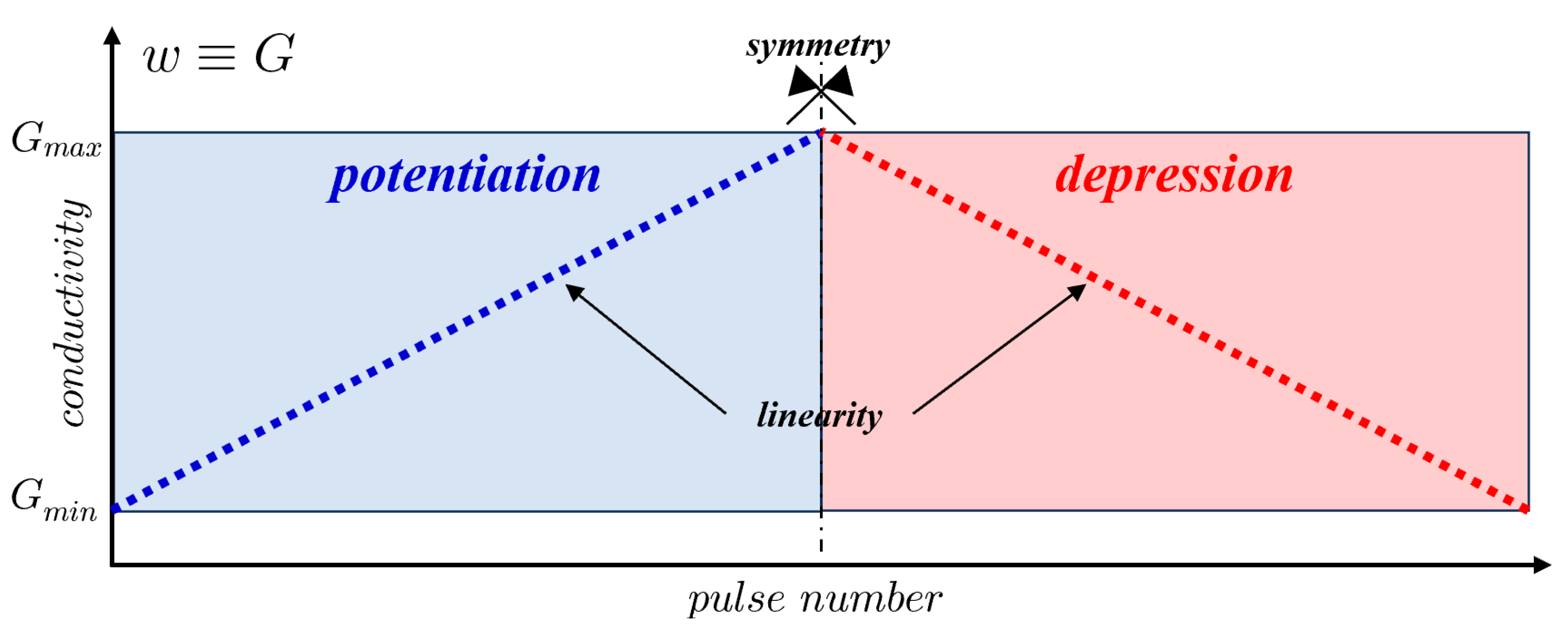
2. RRAM as a Synaptic Element

One of the main applications of RRAM is as a synaptic element in neuromorphic hardware, where the tunable conductance state of the device is used as a synaptic weight (w). This synaptic weight can be modified by different approaches so that the conductance of the RRAM is adapted following the synaptic plasticity rules. According to the number of conductance levels, neural networks can be implemented based on binary [23], multilevel [24] or analog synaptic weights [25]. Neural networks based on binary conductance levels (HRS and LRS) have shown great computing potential and ease of implementation, becoming a suitable option in off-line training, and have been exploited in applications such as associative memories [26]. However, multilevel, where RRAM devices represent more than two discrete conductance levels, and analog, where RRAM devices represent an ideal continuous range of conductance values, weights are preferred for high accurate neural networks. Multilevel and analog weights can be implemented based on the weight update, where the conductivity modulation is focused on a relative change rather than on an absolute conductance value. The weight update behavior is used in on-line training of neural networks and has a strong impact on the learning accuracy of the network [27]. Therefore, modifying the conductance with respect to the programming pulses is critical. Efficient learning requires that the conductance state be linearly increased (potentiation) or decreased (depression) with the application of a programming pulse. Furthermore, high symmetry, where a similar change in conductance is obtained under a positive (potentiation) and negative (depression) pulse, is also desired. Figure 1 shows the desired behavior of a synaptic element [17]. The application of a single programming pulse typically results in a significant variation in conductance [28], becoming unfeasible for synaptic weight storage. For this reason, alternative approaches based on the application of a set of pulses were explored to tune the conductivity of RRAM devices as synaptic elements. A simple programming approach consisted in applying trains of identical voltage pulses to tune the conductivity (see Figure 2a). Some works demonstrated that the application of a train of identical weak pulses may induce a gradual conductance transition useful for analog weight update operations [29,30]. Nevertheless, the conductance rate was not constant, deriving a nonlinear behavior with different evaluations during potentiation and depression [31,32]. Furthermore, an abrupt SET was typically observed in these devices, complicating the tuning of the conductivity [33].
Alternative programming schemes were proposed following the idea of applying identical pulses, but modifying the pattern, to improve the behavior during potentiation. One method consisted in introducing a long weak SET pulse before the typical SET (see Figure 2b). It was reported that this pulse heated the device, improving the analog dynamic range, leading thus to a suppression of the saturation behavior and a more incremental and linear response [34]. A different approach was proposed in [33,35], where a weak RESET pulse was applied just after the SET pulse during potentiation (see Figure 2c). This weak RESET partially disconnected the filament formed by the SET pulse, deriving an intermediate conductance state, improving the response.
Programming strategies were also proposed based on the application of nonidentical pulses, modifying either the amplitude (Figure 3a) or the width (Figure 3b), to improve the synaptic behavior of RRAM devices [31,32]. Nevertheless, these programming methods still resulted in high conductance variability. Alternative programming methodologies also considered RRAM devices integrated in 1T1R arrays. This cell is suitable to avoid sneak path issues at the expense of worse scalability. An example of a 1T1R cell is shown in Figure 4a. Based on this topology, different programming algorithms were proposed exploiting the use of the integrated transistor to decrease variability during potentiation [33,36]. The first approach applied voltage pulses with incremental amplitude to the top electrode (TE) terminal of the 1T1R cell, while the gate voltage of the transistor was maintained constant to control the current compliance, as shown in Figure 4b. In the second approach, the TE voltage was kept to a fixed value, while the gate voltage of the transistor was increased until the desired conductance level was reached. This is shown in Figure 4c.
Voltage-based methodologies have not yet obtained the required performance in terms of symmetry and linearity. For this purpose, recent methodologies have also explored the use of current pulses to overcome the limitations of classical approaches based on voltage pulses, even though it may derive a more complex circuitry. The programming schemes applying identical pulses and nonidentical pulses with increasing current amplitude are shown in Figure 5a and b, respectively. In [37], a train of constant current pulses was applied to achieve positive feedback during depression whereas voltage pulses were applied during potentiation. They reported that this hybrid scheme improved the symmetry of the conductance change in both potentiation and depression. The authors of [38] studied the control of intermediate conductance levels in RRAM devices applying current pulses. Their results showed that using current pulses was valuable to obtain linear potentiation characteristics. However, it was not feasible to obtain the depression characteristic due to the abrupt RESET transition.

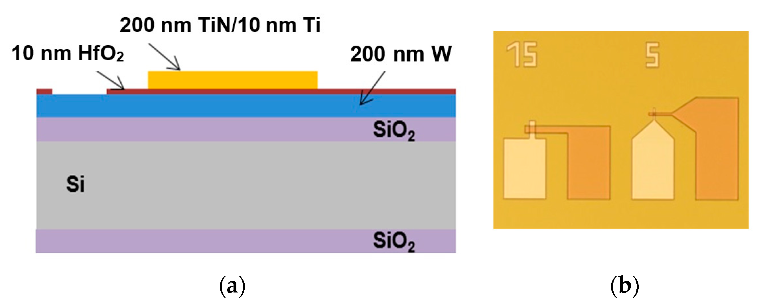
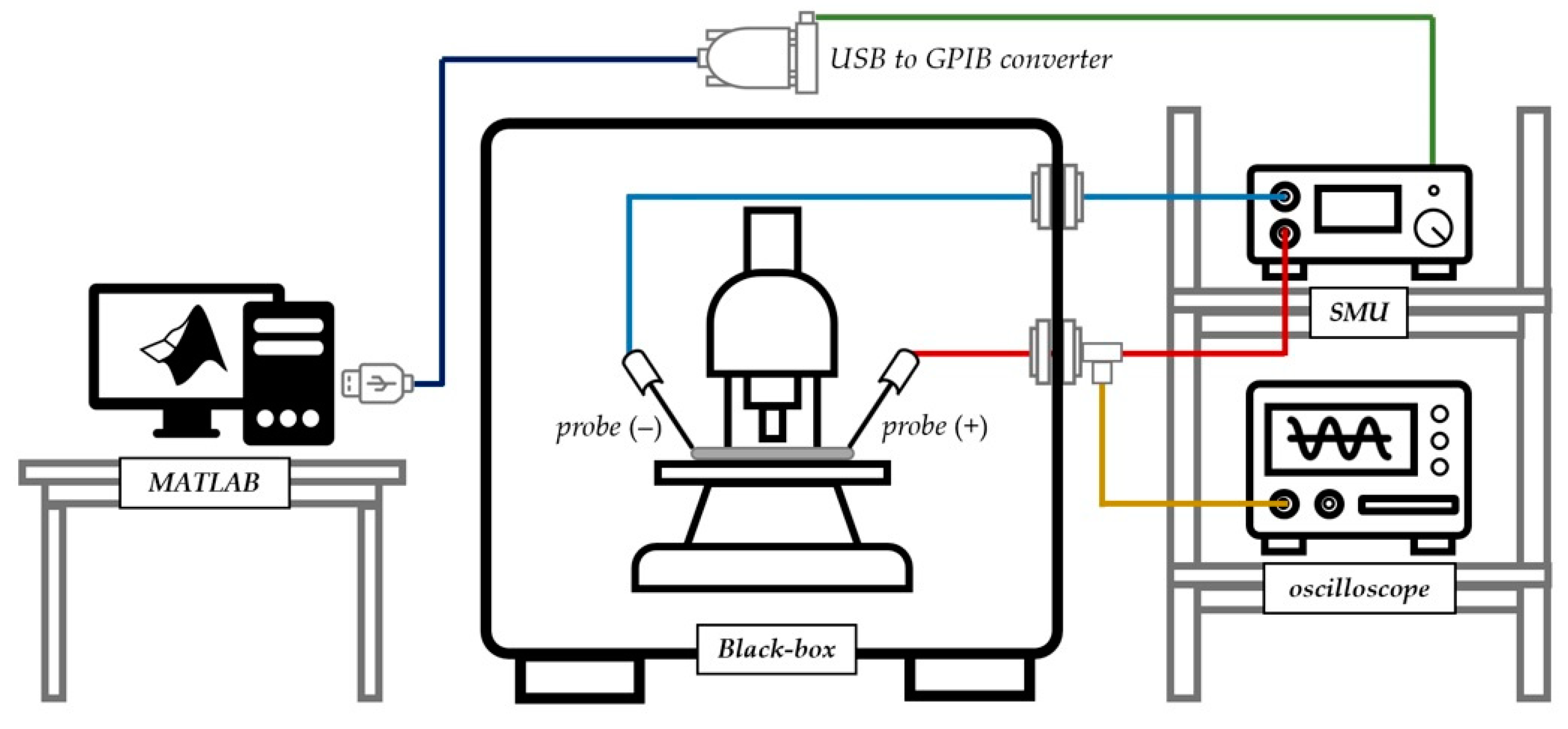
3. Materials and Methods

The RRAM devices considered throughout this work were TiN/Ti/HfO2/W structures [39,40], where the 10 nm thick dielectric film (HfO2) was deposited by atomic layer deposition (ALD) at 225 °C using TDMAH and H2O as precursors. The top electrode consisted of a 200 nm TiN layer and the bottom electrode of a 200 nm W layer. Both metal electrodes were deposited by magnetron sputtering. The 10 nm Ti layer acted as oxygen getter material. A schematic cross-section of the final device structure is shown in Figure 6a. The resulting structures used in the experiments were square cells of 15 × 15 μm2 and 5 × 5 μm2 (see Figure 6b).
The electrical characterization of the devices was performed using a B2912A precision source/measure unit (SMUs, Keysight, Santa Rosa, CA, USA). The experimental setup is shown in Figure 7. The instrument was connected to a computer via GPIB and controlled using MATLAB R2020b for the automation of the measurements. The oscilloscope was only used to validate the generated signals.

4. Experimental Results

The measurement results obtained using the experimental setup are presented in this section. Different programming pulse schemes were applied for the modulation of the conductivity of RRAM devices. The results were divided into voltage-based and current-based pulse schemes.

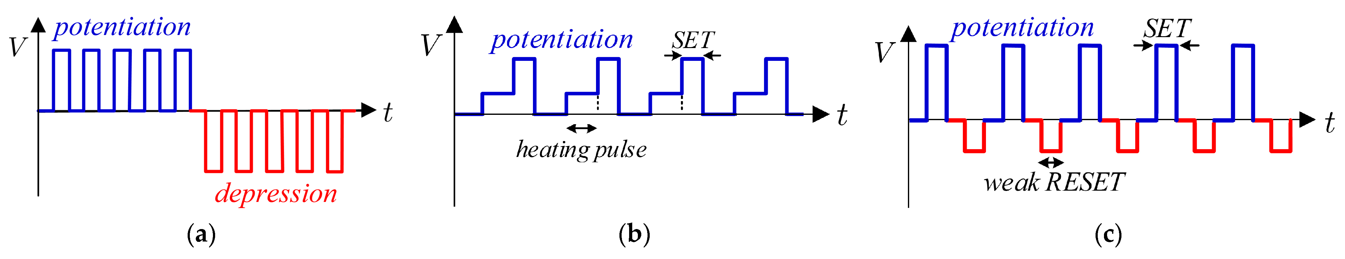
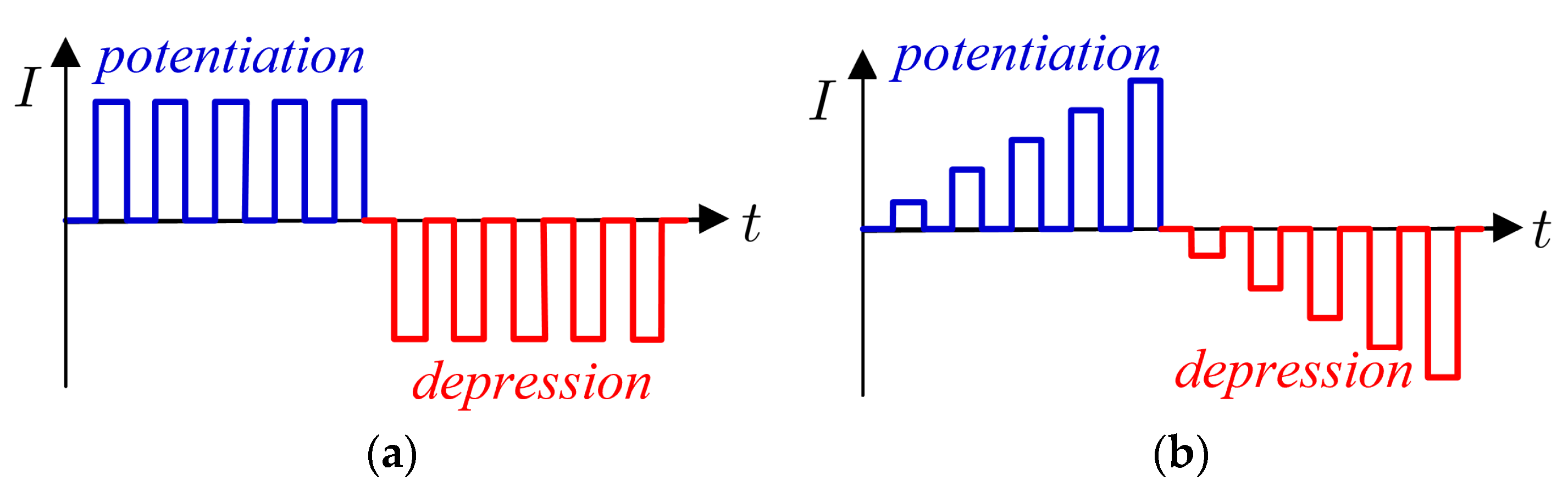
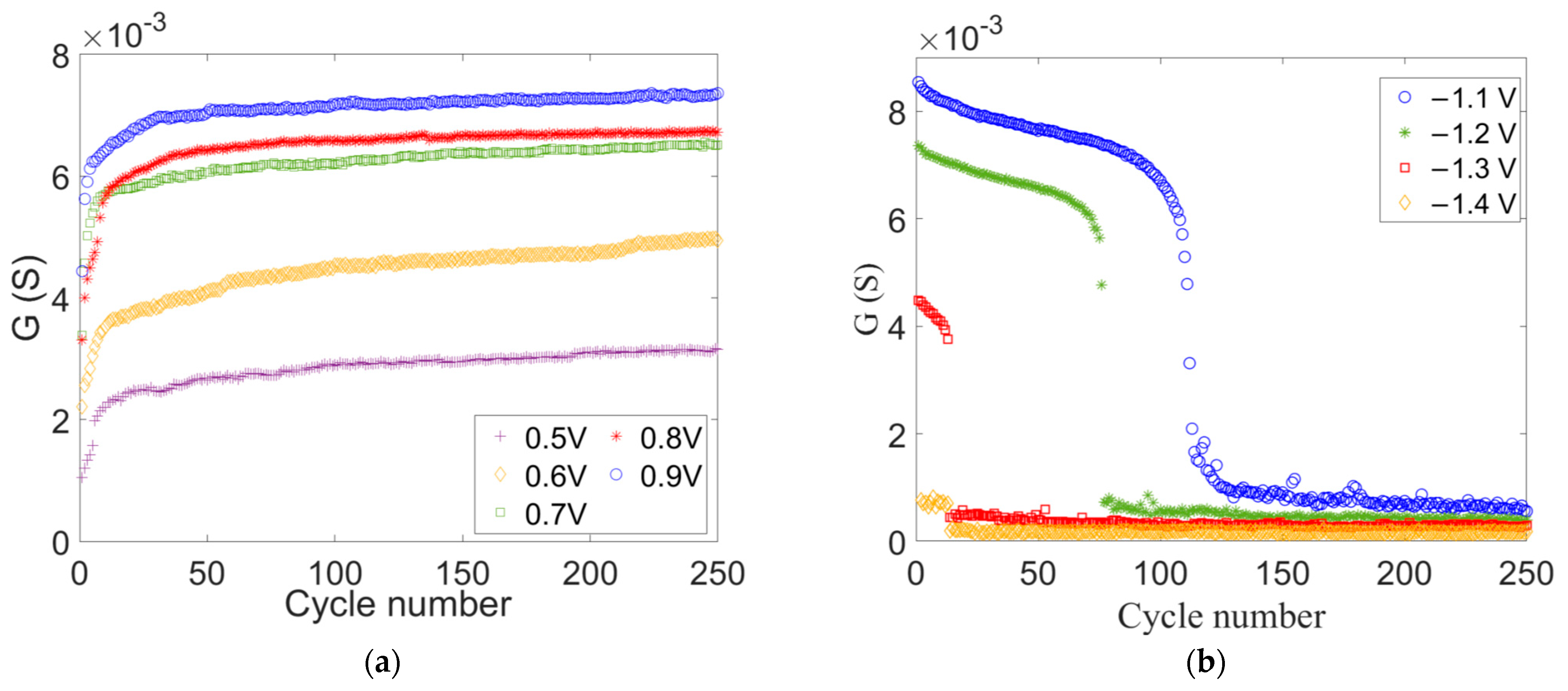
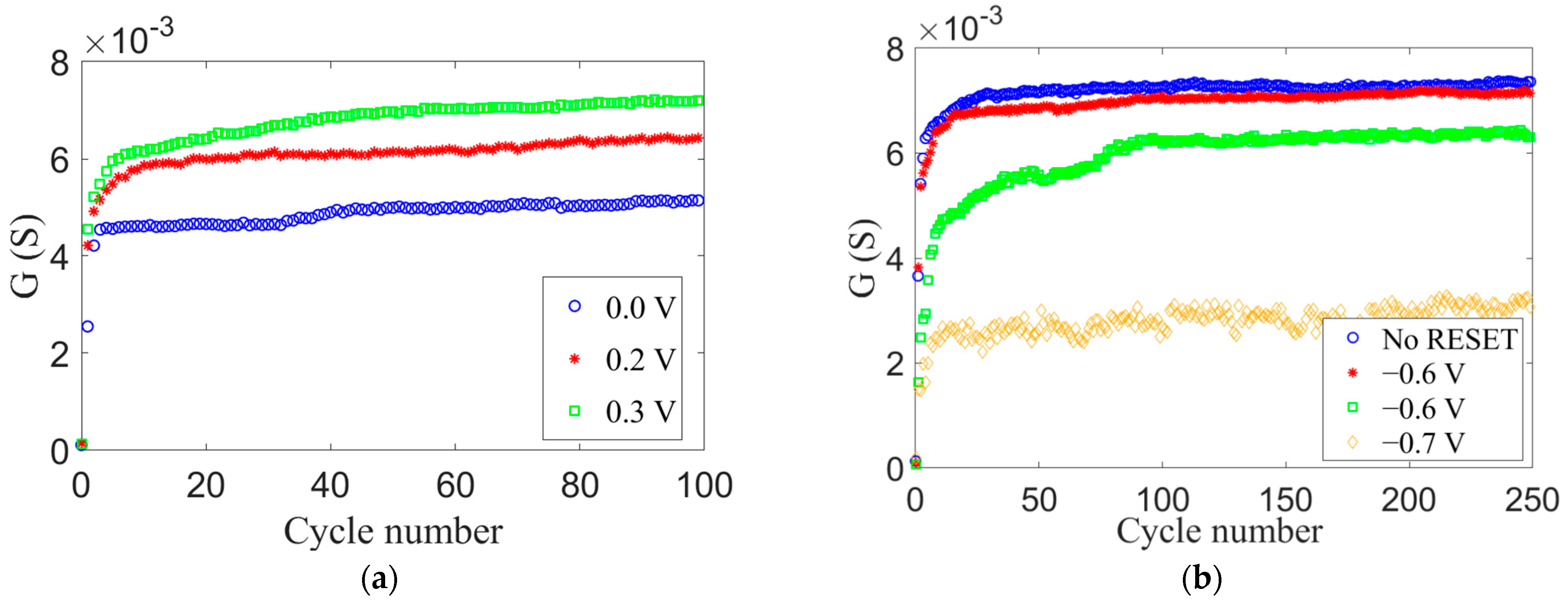
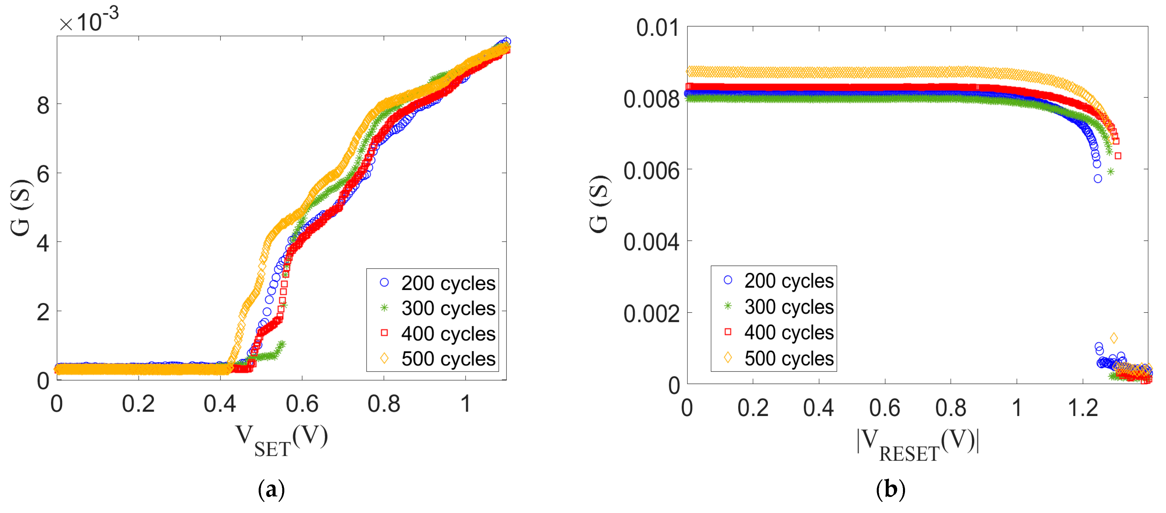
4.1. Voltage Pulse Programming

This section summarizes the experimental results of voltage-based programming techniques. The results were divided into those based on the application of identical pulses and nonidentical pulses.

4.1.1. Identical Pulses

The results related to the application of identical pulses for potentiation and depression, according to the scheme in Figure 2a, are shown in Figure 8. The pulse amplitude was swept to derive the impact of applying different weak pulses. The results for both potentiation (Figure 8a) and depression (Figure 8b) showed that the conductance value of the device gradually changed with the increasing number of pulses (the number of cycles), though a different behavior was observed between both operations. During the SET operation (potentiation), an abrupt transition from HRS to LRS appeared, in a similar manner as reported in other works [33]. This fact is device-dependent. Although the majority of devices typically exhibit an abrupt SET transition, the authors of [31] reported abrupt RESET transitions for their devices. In Figure 8a, it is observed how once this abrupt transition occurred, the conductance increased with a relatively low and almost constant slope (saturation). On the other hand, the RESET (depression) was associated with an initial linear modulation until an abrupt decrease in the conductance set the device in a HRS. Although the results showed the same tendency as in previous works [30,32], the dynamic range in our results was significantly higher. This can be partially explained by narrower pulses used in those works. Anyway, some observations provided valuable insight on the behavior of the devices. During potentiation (Figure 8a), the maximum achievable conductivity depended on the voltage amplitude. However, low increasing conductivity after this abrupt transition seemed to be constant and independent of the pulse amplitude. On the other hand, during depression, the number of cycles required to achieve the abrupt transition to HRS decreased for higher voltage amplitudes (in absolute value). Also, the reduction in the conductance after the first pulse became larger for higher voltage amplitudes. It is worth noting that all the depression curves had a region with a linear-like behavior before the abrupt transition. This provided a potential range of values for the fine tuning of the device, although it does not exploit the whole operating window of the device.
Alternative programming, based on the application of identical pulses to improve the modulation of the conductivity during potentiation, was also conducted. Figure 9a shows the results for the programming technique previously presented in Figure 2b, where a long weak ‘heating’ SET pulse was applied before the typical SET pulse. The results indicated that the linearity and the dynamic range were slightly improved in comparison with the case without the ‘heating’ pulse (shown in blue). This behavior was consistent with the results reported in [34], although the enhancement of the dynamic range was significantly lower in our results (45% against 80% in [34]). However, this improvement was achieved with low amplitudes of the ‘heating’ pulse. Higher values could not be applied without directly influencing the conductivity of the device, since VSET was typically around 0.4 V for this technology.
Another programming scheme based on identical pulses used a compensating weak RESET after the SET pulse during potentiation (see Figure 2c). The results for this technique are shown in Figure 9b. Although intermediate conductance values were derived, no significant improvement was obtained in terms of linearity related to the case where no RESET pulse was applied (in blue), even though different amplitudes were considered for such weak RESET pulse. Both pulses (SET and weak RESET) had the same width as in the optimized case reported in [33].

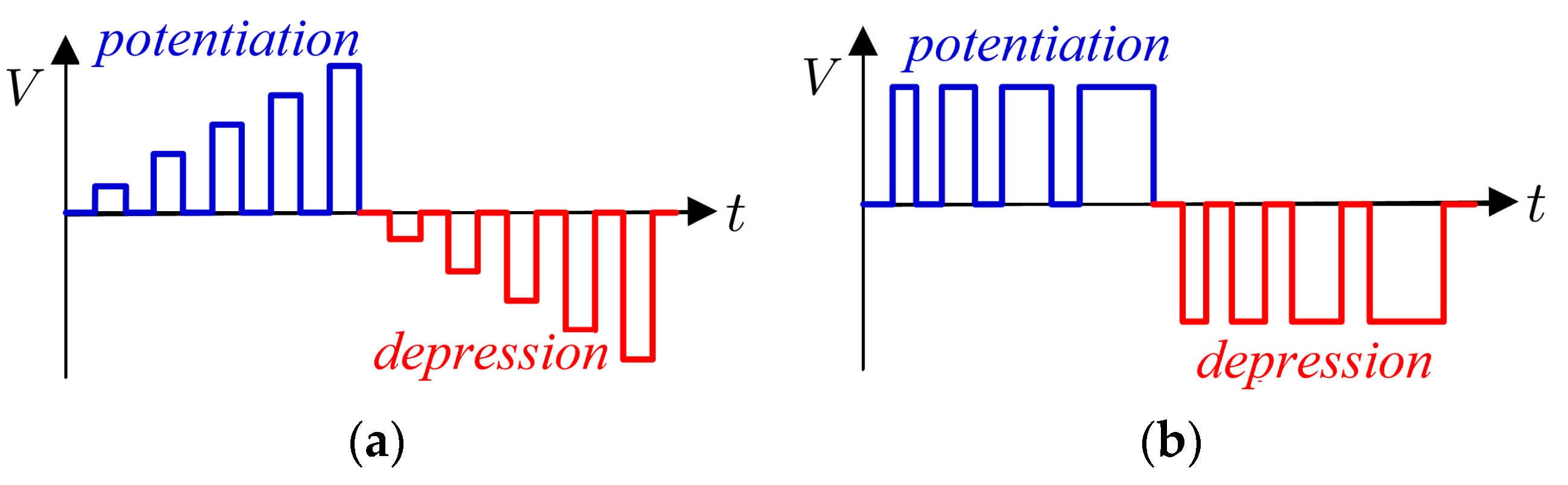
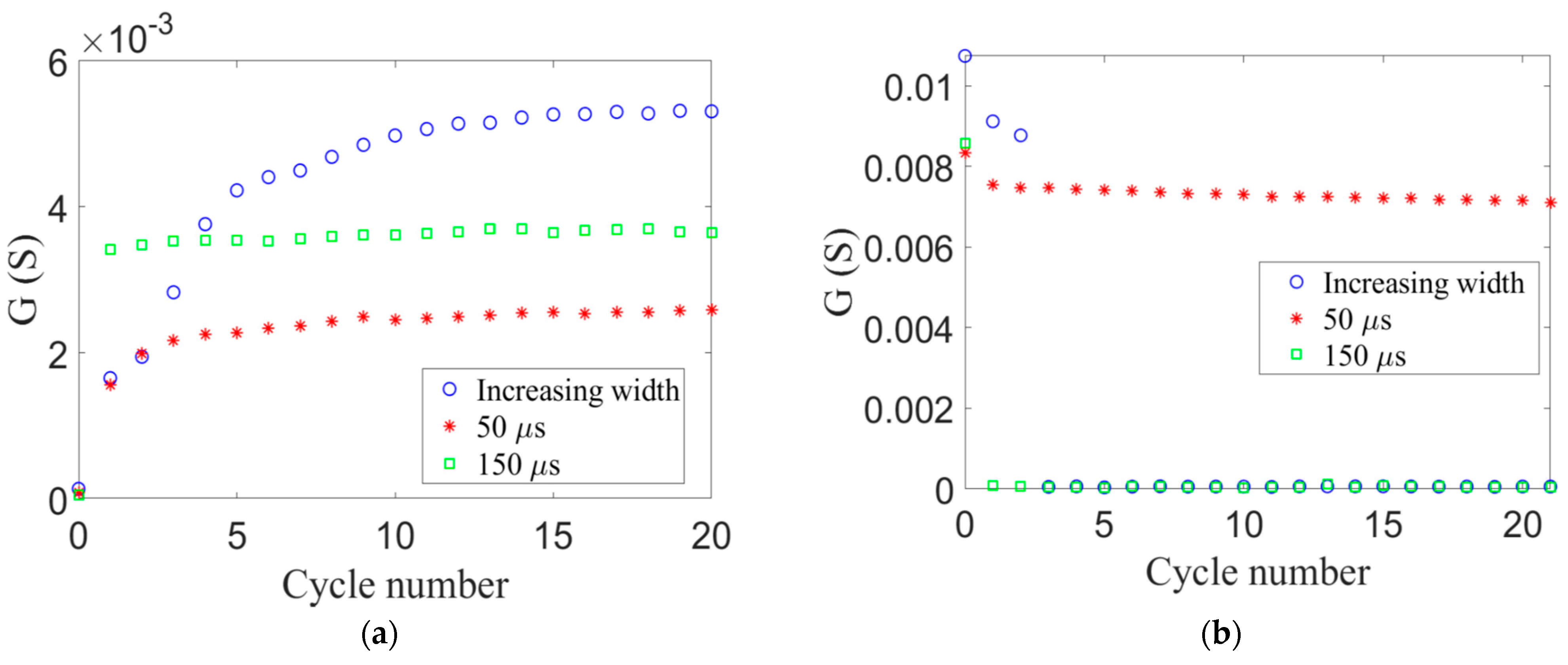
4.1.2. Nonidentical Pulses

This subsection summarizes the results obtained from the application of nonidentical voltage pulses. The first experiment was based on the scheme previously presented in Figure 4b, where the pulse amplitude was incremented at each cycle. The amplitude was incremented from 0 V to 1.1 V during potentiation and from 0 V to −1.4 V during depression. The results are summarized in Figure 10. It shows that the initial HRS (during potentiation) or LRS (during depression) is not modified until a certain voltage threshold is surpassed. During potentiation, this value was around 0.4 V while during depression −1.0 V. These values were consistent with the typical VSET and VRESET for which the switch from HRS to LRS and from LRS to HRS was induced, respectively. The results are in agreement with those reported in [32]. As for the shape, Figure 10a shows a linear-like behavior, similar to what is desired for the fine tuning of the device, although its profile presented fluctuations which prevented it from reaching a complete linear behavior. During depression (Figure 10b), there was an abrupt transition to HRS with low tuning of intermediate conductance values. It can be finally observed that for both the potentiation and depression, the total number of cycles did not have a strong impact on the results; i.e., the increasing step of the pulse amplitude did not significantly affect the modulation of the conductivity.
An experiment was also conducted where the pulse width was incremented at each cycle. The results are summarized in Figure 11a,b for potentiation and depression, respectively. For potentiation (Figure 11a), a slight improvement in terms of linearity and dynamic range related to applying pulses with constant width was observed. On the other hand, no modulation of the conductivity was registered during depression (Figure 11b) since an abrupt transition to the HRS occurred.
The target devices did not include an integrated transistor. For that reason, the experiments based on 1T1R cells could not be exactly reproduced. Hence, we emulated the influence of the transistor by limiting the current compliance allowed by the SMU. The modulation of the conductance was then similar to the scheme previously presented in Figure 4c. The results for potentiation are summarized in Figure 12a for different current steps between the minimum (null current) and the maximum allowed current (8 mA). The results showed a similar tendency as in [33], although it is worth noting that time widths, voltages, and the absence of the transistor influenced a difference evolution of the conductance. Anyway, the results resembled a linear modulation of the conductivity, regardless of the number of cycles (the number of current steps) applied. What is more, although the initial (low) conductance state was different for every case, the modulation of the conductivity always followed the same trend. An equivalent experiment was conducted for depression, applying RESET pulses limiting the current compliance. The results are shown in Figure 12b. The conductivity of the device was not modified until an abrupt transition to the HRS was observed. In this case, the tuning of the conductivity did not provide any interesting feature in comparison with the results obtained using the voltage-based schemes.

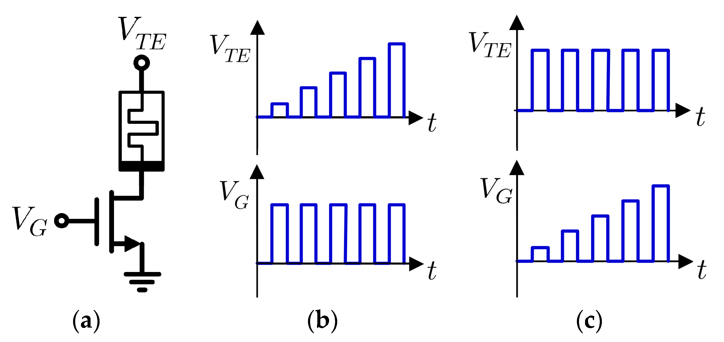
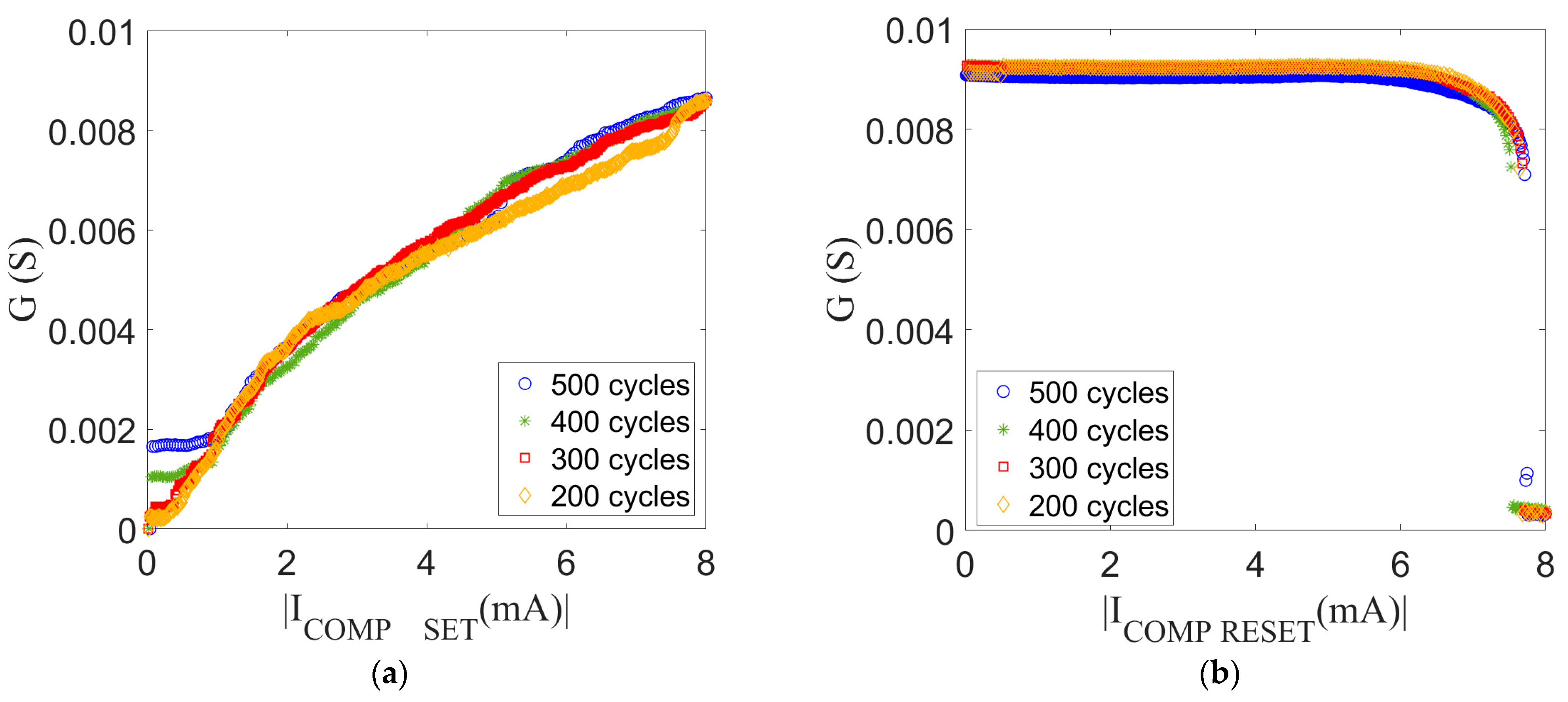
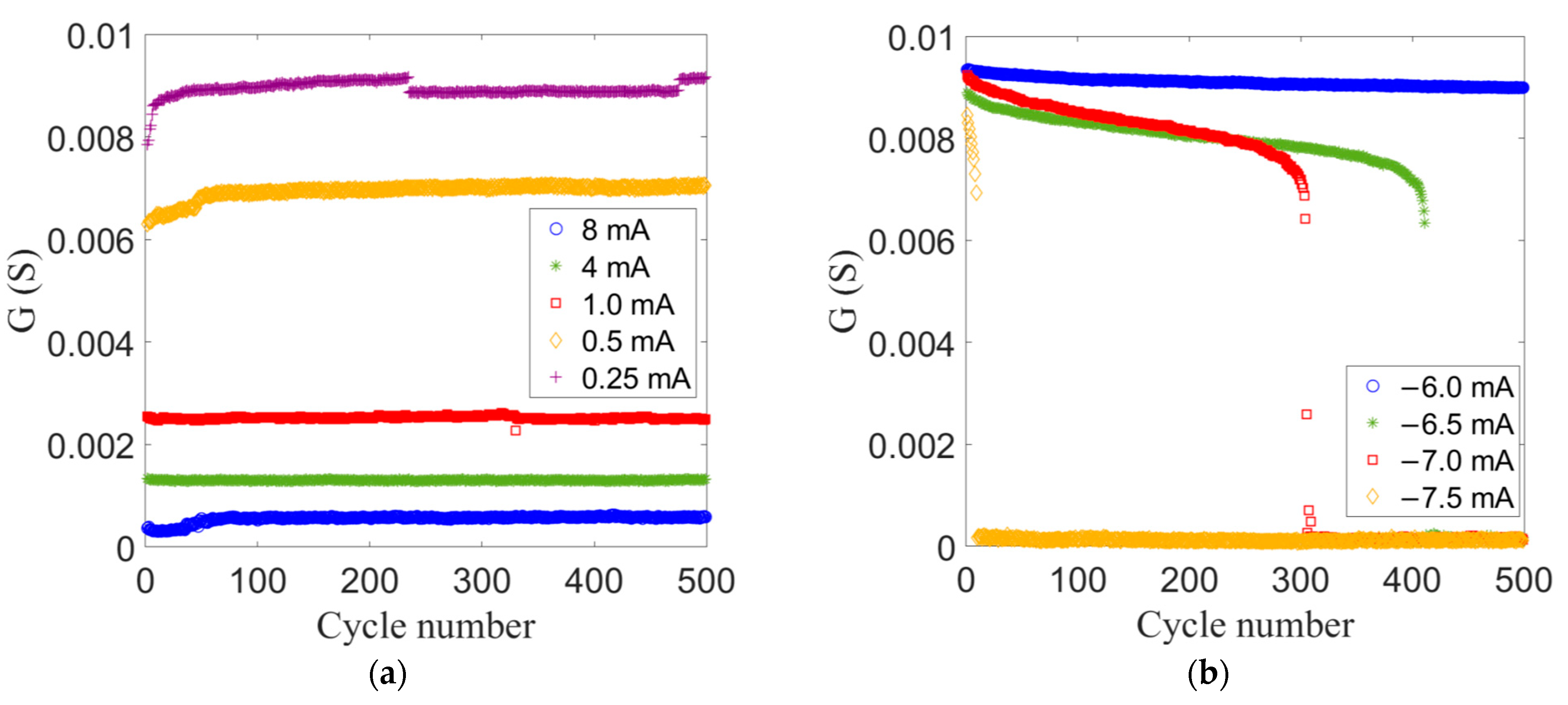
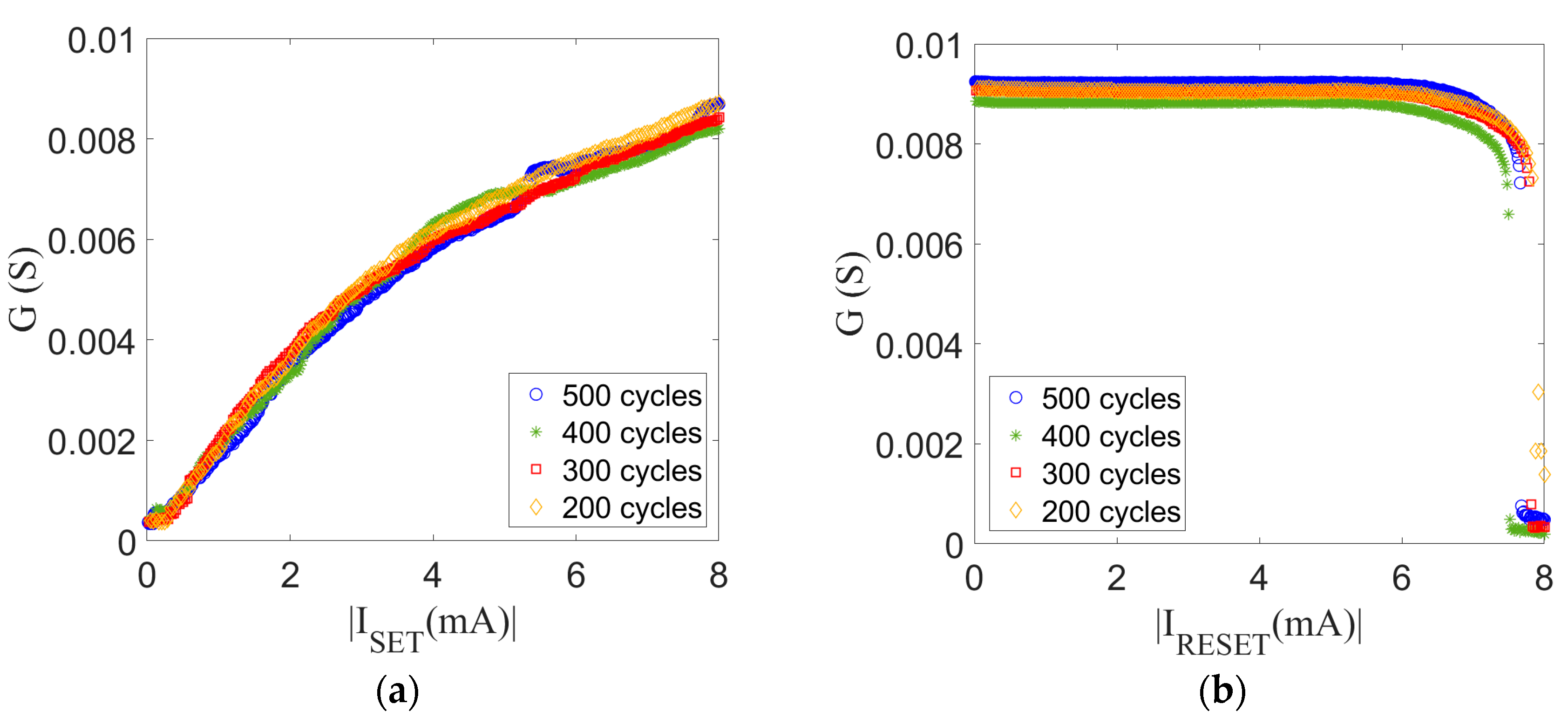
4.2. Current Pulse Programming

This subsection presents the results of modulating the conductivity of RRAM devices based on the current pulses. The first experiment was devoted to the application of equal current pulses. The results are summarized in Figure 13a for potentiation and in Figure 13b for depression. During potentiation, the final conductance value achieved in each case depended on the amplitude of the pulse. There was deficient modulation of the conductivity since the transition from HRS to LRS was abrupt, with a small number of intermediate conductance values. In fact, the final value was achieved with few pulses. These results suggested that applying nonidentical pulses with increasing amplitude could be exploited to improve linearity. On the other hand, the results for depression showed a similar tendency as in the case of constant amplitude voltage pulses (Figure 8b). An initial linear behavior with low slope was observed before an abrupt transition to HRS. Therefore, this may provide a range of conductance values with fine modulation of the conductance before the abrupt transition to the HRS. As expected, the number of cycles required to induce the abrupt switch decreased for increasing amplitudes (in absolute value) of the current pulses. The results obtained during depression differed from those described in [37,38]. The former presented a continuous depression characteristic from LRS to HRS. On the other hand, the depression characteristic was not included in [38] since the devices exhibited abrupt RESET transitions. Our results were halfway between those reported in both works, since there was a range of intermediate values before the abrupt RESET transition appeared.
Finally, an experiment based on the current pulses with increasing amplitude was also conducted. The results shown in Figure 14 were similar to those obtained by limiting the current compliance (Figure 12). The potentiation results (Figure 14a) showed a gradual smooth transition following a linear-like behavior for all the range of the current amplitude values. This could be predicted by the behavior shown for equal current pulses (Figure 13), where the final conductance value was dependent on the amplitude of the pulse. Furthermore, the number of cycles (the increment step of the current amplitude) did not influence the potentiation characteristic. On the other hand, for the depression characteristic (Figure 14b), the conductivity of the device was not modified until an abrupt transition to HRS was observed. Therefore, almost no tuning of the conductivity was reached with this technique. The results in this case were in agreement with those presented in [38].

5. Discussion

This section is devoted to a quantitative analysis of the experimental results of the different programming schemes used to modulate the conductivity of RRAM devices. The results were compared by computing the asymmetric nonlinearity factor (ANL) presented in [41]. This model relates the measured conductance G and the cumulative number of pulses ( n p for potentiation and n d for depression) by the following expressions:
G p ( n p ) = G m i n + A   n p n p + e k
  G d ( n d ) = G m a x A   ( N n d ) ( N n d ) + e k
where Gp and Gd are the functions describing the conductance of potentiation and depression curves, respectively, Gmin and Gmax are the minimum and maximum values of the conductance, N is the total number of pulses, and k is the fitting parameter. A in turn is given by the following expression:
A = G m a x G m i n   1 + e k N
Moreover, the asymmetric nonlinearity factor (ANL) is defined as follows:
A N L = G p N 2 G d N 2 / G m a x G m i n
where complete symmetry and linearity are achieved when ANL = 0, and the maximum nonlinearity is achieved when ANL = 1. Nonetheless, we intended to evaluate each technique individually for potentiation and depression. Hence, full symmetry with the inverse technique was considered. Therefore, in this case, the ANL value exclusively represented the nonlinearity of the results achieved with each technique. The best fitting parameter for each technique was then found by minimizing the mean value of the squared difference between each conductance value obtained experimentally and the corresponding conductance value predicted by the model for each pulse. Thus, this method provided a quantitative analysis for each result so as to determine which, amongst the different approaches discussed in this paper, was the most suitable technique to achieve the desired behavior of a synaptic element. However, the implications in terms of circuitry and implementation of these techniques were beyond the scope of the work.
The predictions of the ANL parameter are summarized in Table 1. The difference GminGmax is also included. According to the results, three modulation techniques were the most suitable for potentiation, having similar ANL values: the incremental voltage amplitude, limiting current and incremental current amplitude techniques. Notice how the same techniques also produced the highest values for GminGmax. Among the three options, the incremental voltage amplitude techniques had the worst ANL value. Additionally, it had the drawback of a nonuniform modulation for the whole range of voltage values, since a minimum voltage was required to start modulating the conductance, as shown in Figure 10a. Regarding the incremental current amplitude and limiting current techniques, the latter offers, in theory, the benefit of easier circuit implementation. Overall, it can be concluded that the techniques that are based on incremental pulse amplitudes had the best performance during potentiation in terms of linearity.
Regarding the depression results, the techniques with identical current pulses had a significantly better ANL coefficient compared to the alternatives. It must be noted that the ANL was computed over the range of pulses before the abrupt transition took place. Furthermore, some of the schemes exhibited such poor behavior in terms of linearity that they could not be evaluated by the model, and, therefore, they were discarded. Consequently, during depression, the techniques applying identical pulses produced the best results.

6. Conclusions

RRAM is an outstanding candidate as a synaptic element in neural networks due to its excellent scalability, fast switching speed, multilevel capability, low power programming and CMOS compatibility. However, there are still some challenges that need to be solved so that RRAM devices fulfill the requirements of an analog synapse. A primary concern is related to linear and symmetrical conductance changes. Extensive research effort is devoted at different levels to overcome this issue. In fact, different programming schemes have been explored for that purpose. This work examines various of these programming techniques aimed at controlling the conductive properties of RRAM devices, with the goal of utilizing them as synaptic components. Experimental measurements were carried out on the same RRAM devices across diverse programming schemes. A comparison among the different techniques was conducted by computing the asymmetric nonlinearity factor. The best results were obtained for the incremental current amplitude and limiting current techniques during potentiation and for the technique applying identical current pulses during depression. These results must be combined with other considerations, such as the ease of implementation and complexity of the circuitry, to finally determine the most suitable programming technique. In any case, this work is intended to provide guidance for future research devoted to improving the performance of RRAM devices for synaptic application in neural networks.

Author Contributions

Conceptualization, D.A. and S.M.; methodology, P.M. and D.A.; software, P.M., D.A. and Á.G.-P.; validation, P.M. and D.A.; formal analysis, D.A. and R.R.-M.; investigation, P.M.; resources, R.R.-M., M.B.G. and F.C.; data curation, P.M.; writing—original draft preparation, P.M. and D.A.; writing—review and editing, S.M., Á.G.-P., M.B.G. and F.C.; funding acquisition, R.R.-M. All authors have read and agreed to the published version of the manuscript.

Funding

This work was supported in part by Spanish MCIN/AEI /10.13039/501100011033/FEDER, under Projects PID2022-141391OB-C22 and PID2022-139586NB-C42.

Data Availability Statement

Data are contained within the article.

Conflicts of Interest

The authors declare no conflict of interest.

References

  1. Furber, S. Large-scale neuromorphic computing systems. J. Neural Eng. 2016, 13, 051001. [Google Scholar] [CrossRef]
  2. Misra, J.; Saha, I. Artificial neural networks in hardware: A survey of two decades of progress. Neurocomputing 2010, 74, 239–255. [Google Scholar] [CrossRef]
  3. Yu, S.; Li, Z.; Chen, P.-Y.; Wu, H.; Gao, B.; Wang, D.; Wu, W.; Qian, H. Binary neural network with 16 Mb RRAM macro chip for classification and online training. In Proceedings of the 2016 IEEE International Electron Devices Meeting (IEDM), San Francisco, CA, USA, 3–7 December 2016; pp. 16.2.1–16.2.4. [Google Scholar] [CrossRef]
  4. Burr, G.W.; Shelby, R.M.; Sebastian, A.; Kim, S.; Kim, S.; Sidler, S.; Virwani, K.; Ishii, M.; Narayanan, P.; Fumarola, A.; et al. Neuromorphic computing using non-volatile memory. Adv. Phys. X 2016, 2, 89–124. [Google Scholar] [CrossRef]
  5. Ni, Y.; Zhang, S.; Sun, L.; Liu, L.; Wei, H.; Xu, Z.; Xu, W.; Xu, W. A low-dimensional hybrid p-i-n heterojunction neuromorphic transistor with ultra-high UV sensitivity and immediate switchable plasticity. Appl. Mater. Today 2021, 25, 101223. [Google Scholar] [CrossRef]
  6. Ni, Y.; Liu, L.; Liu, J.; Xu, W. A High-Strength Neuromuscular System That Implements Reflexes as Controlled by a Multiquadrant Artificial Efferent Nerve. ACS Nano 2022, 16, 20294–20304. [Google Scholar] [CrossRef]
  7. Sun, Y.; Li, J.; Li, S.; Jiang, Y.; Wan, E.; Zhang, J.; Shi, Y.; Pan, L. Advanced synaptic devices and their applications in biomimetic sensory neural system. Chip 2023, 2, 100031. [Google Scholar] [CrossRef]
  8. Ielmini, D.; Ambrogio, S. Emerging neuromorphic devices. Nanotechnology 2019, 31, 092001. [Google Scholar] [CrossRef]
  9. Lanza, M.; Wong, H.-S.P.; Pop, E.; Ielmini, D.; Strukov, D.; Regan, B.C.; Larcher, L.; Villena, M.A.; Yang, J.J.; Goux, L.; et al. Recommended methods to study resistive switching devices. Adv. Electron. Mater. 2019, 5, 1800143. [Google Scholar] [CrossRef]
  10. Wong, H.S.P.; Lee, H.Y.; Yu, S.; Chen, Y.S.; Wu, Y.; Chen, P.S.; Lee, B.; Chen, F.T.; Tsai, M.J. Metal–oxide RRAM. Proc. IEEE 2012, 100, 1951–1970. [Google Scholar] [CrossRef]
  11. Yu, S.; Guan, X.; Wong, H.-S.P. On the stochastic nature of resistive switching in metal oxide RRAM: Physical Modeling, Monte Carlo simulation, and experimental characterization. In Proceedings of the 2011 International Electron Devices Meeting (IEDM), Washington, DC, USA, 5–7 December 2011; pp. 17.3.1–17.3.4. [Google Scholar] [CrossRef]
  12. Grossi, A.; Vianello, E.; Sabry, M.M.; Barlas, M.; Grenouillet, L.; Coignus, J.; Beigne, E.; Wu, T.; Le, B.Q.; Wootters, M.K.; et al. Resistive RAM Endurance: Array-Level Characterization and Correction Techniques Targeting Deep Learning Applications. IEEE Trans. Electron Devices 2019, 66, 1281–1288. [Google Scholar] [CrossRef]
  13. Lee, M.J.; Lee, C.B.; Lee, D.; Lee, S.R.; Chang, M.; Hur, J.H.; Kim, Y.B.; Kim, C.J.; Seo, D.H.; Seo, S.; et al. A fast, high-endurance and scalable non-volatile memory device made from asymmetric Ta2O5− x/TaO2− x bilayer structures. Nat. Mater. 2011, 10, 625–630. [Google Scholar] [CrossRef] [PubMed]
  14. Wu, W.; Wu, H.; Gao, B.; Yao, P.; Zhang, X.; Peng, X.; Yu, S.; Qian, H. A Methodology to Improve Linearity of Analog RRAM for Neuromorphic Computing. In Proceedings of the 2018 IEEE Symposium on VLSI Technology, Honolulu, HI, USA, 18–22 June 2018; pp. 103–104. [Google Scholar]
  15. Choi, S.; Yang, J.; Wang, G. Emerging memristive artificial synapses and neurons for energy-efficient neuromorphic computing. Adv. Mater. 2020, 32, e2004659. [Google Scholar] [CrossRef] [PubMed]
  16. Li, Y.; Ang, K.-W. Hardware implementation of neuromorphic computing using large-scale memristor crossbar arrays. Adv. Intell. Syst. 2020, 3, 2000137. [Google Scholar] [CrossRef]
  17. Woo, J.; Yu, S. Resistive Memory-Based Analog Synapse: The Pursuit for Linear and Symmetric Weight Update. IEEE Nanotechnol. Mag. 2018, 12, 36–44. [Google Scholar] [CrossRef]
  18. Ye, N.; Cao, L.; Yang, L.; Zhang, Z.; Fang, Z.; Gu, Q.; Yang, G.-Z. Improving the robustness of analog deep neural networks through a Bayes-optimized noise injection approach. Commun. Eng. 2023, 2, 25. [Google Scholar] [CrossRef]
  19. Liu, T.; Wen, W.; Jiang, L.; Wang, Y.; Yang, C.; Quan, G. A Fault-Tolerant Neural Network Architecture. In Proceedings of the 2019 56th ACM/IEEE Design Automation Conference (DAC), Las Vegas, NV, USA, 2–6 June 2019; pp. 1–6. [Google Scholar]
  20. Ye, N.; Mei, J.; Fang, Z.; Zhang, Y.; Zhang, Z.; Wu, H.; Liang, X. BayesFT: Bayesian Optimization for Fault Tolerant Neural Network Architecture. In Proceedings of the 2021 58th ACM/IEEE Design Automation Conference (DAC), San Francisco, CA, USA, 5–9 December 2021; pp. 487–492. [Google Scholar]
  21. Shen, Z.; Zhao, C.; Qi, Y.; Xu, W.; Liu, Y.; Mitrovic, I.Z.; Yang, L.; Zhao, C. Advances of RRAM Devices: Resistive Switching Mechanisms, Materials and Bionic Synaptic Application. Nanomaterials 2020, 10, 1437. [Google Scholar] [CrossRef]
  22. Lammie, C.; Azghadi, M.R. MemTorch: A Simulation Framework for Deep Memristive Cross-Bar Architectures. In Proceedings of the 2020 IEEE International Symposium on Circuits and Systems (ISCAS), Seville, Spain, 10–21 October 2020; pp. 1–5. [Google Scholar]
  23. Türel, O.; Likharev, K. CrossNets: Possible neuromorphic networks based on nanoscale components. Int. J. Circuit Theory Appl. 2003, 31, 37–53. [Google Scholar] [CrossRef]
  24. Minnekhanov, A.A.; Emelyanov, A.V.; Lapkin, D.A.; Nikiruy, K.E.; Shvetsov, B.S.; Nesmelov, A.A.; Rylkov, V.V.; Demin, V.A.; Erokhin, V.V. Parylene based memristive devices with multilevel resistive switching for neuromorphic applications. Sci. Rep. 2019, 9, 10800. [Google Scholar] [CrossRef]
  25. Wu, W.; Wu, H.; Gao, B.; Deng, N.; Yu, S.; Qian, H. Improving Analog Switching in HfOx-Based Resistive Memory with a Thermal Enhanced Layer. IEEE Electron Device Lett. 2017, 38, 1019–1022. [Google Scholar] [CrossRef]
  26. Alibart, F.; Sherwood, T.; Strukov, D.B. Hybrid CMOS/nanodevice circuits for high throughput pattern matching applications. In Proceedings of the 2011 NASA/ESA Conference on Adaptive Hardware and Systems (AHS), San Diego, CA, USA, 6–9 June 2011; pp. 279–286. [Google Scholar]
  27. Yu, S.; Chen, P.-Y.; Cao, Y.; Xia, L.; Wang, Y.; Wu, H. Scaling-up resistive synaptic arrays for neuro-inspired architecture: Challenges and prospect. In Proceedings of the 2015 IEEE International Electron Devices Meeting (IEDM), Washington, DC, USA, 7–9 December 2015; pp. 17.3.1–17.3.4. [Google Scholar]
  28. Ambrogio, S.; Balatti, S.; Cubeta, A.; Calderoni, A.; Ramaswamy, N.; Ielmini, D. Statistical Fluctuations in HfOx Resistive-Switching Memory: Part I-Set/Reset Variability. IEEE Trans. Electron Devices 2014, 61, 2912–2919. [Google Scholar] [CrossRef]
  29. Yao, P.; Wu, H.; Gao, B.; Eryilmaz, S.B.; Huang, X.; Zhang, W.; Zhang, Q.; Deng, N.; Shi, L.; Wong, H.-S.P.; et al. Face classification using electronic synapses. Nat. Commun. 2017, 8, 15199. [Google Scholar] [CrossRef] [PubMed]
  30. Frascaroli, J.; Brivio, S.; Covi, E.; Spiga, S. Evidence of soft bound behaviour in analogue memristive devices for neuromorphic computing. Sci. Rep. 2018, 8, 7178. [Google Scholar] [CrossRef] [PubMed]
  31. Park, S.; Sheri, A.; Kim, J.; Noh, J.; Jang, J.; Jeon, M.; Lee, B.; Hwang, H. Neuromorphic speech systems using advanced ReRAM-based synapse. In Proceedings of the 2013 IEEE International Electron Devices Meeting (IEDM), Washington, DC, USA, 9–11 December 2013; pp. 25.6.1–25.6.4. [Google Scholar]
  32. Covi, E.; Brivio, S.; Serb, A.; Prodromakis, T.; Fanciulli, M.; Spiga, S. Analog memristive synapse in spiking networks implementing unsupervised learning. Front. Neurosci. 2016, 10, 482. [Google Scholar] [CrossRef] [PubMed]
  33. Woo, J.; Moon, K.; Song, J.; Kwak, M.; Park, J.; Hwang, H. Optimized programming scheme enabling linear potentiation in filamentary hfo2 rram synapse for neuromorphic systems. IEEE Trans. Electron Devices 2016, 63, 5064–5067. [Google Scholar] [CrossRef]
  34. Jeong, Y.; Kim, S.; Lu, W.D. Utilizing multiple state variables to improve the dynamic range of analog switching in a memristor. Appl. Phys. Lett. 2015, 107, 173105. [Google Scholar] [CrossRef]
  35. Wang, I.-T.; Chang, C.-C.; Chiu, L.-W.; Chou, T.; Hou, T.-H. 3D Ta/TaOx/TiO2/Ti synaptic array and linearity tuning of weight update for hardware neural network applications. Nanotechnology 2016, 27, 365204–365212. [Google Scholar] [CrossRef] [PubMed]
  36. Milo, V.; Anzalone, F.; Zambelli, C.; Perez, E.; Mahadevaiah, M.K.; Ossorio, O.G.; Olivo, P.; Wenger, C.; Ielmini, D. Optimized programming algorithms for multilevel RRAM in hardware neural networks. In Proceedings of the 2021 IEEE International Reliability Physics Symposium (IRPS), Monterey, CA, USA, 21–25 March 2021; pp. 1–6. [Google Scholar]
  37. Park, J.; Kwak, M.; Moon, K.; Woo, J.; Lee, D.; Hwang, H. TiOx-based RRAM synapse with 64-levels of conductance and symmetric conductance change by adopting a hybrid pulse scheme for neuromorphic computing. IEEE Electron Device Lett. 2016, 37, 1559–1562. [Google Scholar] [CrossRef]
  38. Garcia, H.; Duenas, S.; Ossorio, O.G.; Castan, H. Current Pulses to Control the Conductance in RRAM Devices. IEEE J. Electron Devices Soc. 2020, 8, 291–296. [Google Scholar] [CrossRef]
  39. Arumí, D.; Gómez-Pau, Á.; Manich, S.; Rodríguez-Montañés, R.; González, M.B.; Campabadal, F. Unpredictable bits generation based on RRAM parallel configuration. IEEE Electron Device Lett. 2018, 40, 341–344. [Google Scholar] [CrossRef]
  40. Arumí, D.; Gonzalez, M.; Campabadal, F. RRAM serial configuration for the generation of random bits. Microelectron. Eng. 2017, 178, 76–79. [Google Scholar] [CrossRef]
  41. Chang, C.-C.; Chen, P.-C.; Chou, T.; Wang, I.-T.; Hudec, B.; Chang, C.-C.; Tsai, C.-M.; Chang, T.-S.; Hou, T.-H. Mitigating Asymmetric Nonlinear Weight Update Effects in Hardware Neural Network Based on Analog Resistive Synapse. IEEE J. Emerg. Sel. Top. Circuits Syst. 2017, 8, 116–124. [Google Scholar] [CrossRef]
Figure 1. Ideal behavior of a synaptic element where conductance is expressed as G on the Y-axis.
Electronics 12 04803 g001
Figure 2. Voltage-based programming scheme: (a) potentiation and depression applying identical pulses; (b) long weak SET pulse preceding the SET pulse during potentiation; (c) weak RESET pulse following the SET pulse during potentiation.
Electronics 12 04803 g002
Figure 3. Voltage-based programming scheme for potentiation and depression applying nonidentical pulses: (a) with increasing amplitude; (b) with increasing width.
Electronics 12 04803 g003
Figure 4. Voltage-based programming schemes based on 1T1R cell: (a) schematic; (b) potentiation applying nonidentical pulses with increasing amplitude to TE; (c) potentiation applying nonidentical pulses with increasing amplitude to the gate terminal of the transistor.
Electronics 12 04803 g004
Figure 5. Current-based programming scheme for potentiation and depression: (a) identical pulses; (b) nonidentical pulses with increasing amplitude.
Electronics 12 04803 g005
Figure 6. RRAM devices: (a) schematic cross-section; (b) top view optical microscope image.
Electronics 12 04803 g006
Figure 7. Experimental setup showcasing the connections between the probes and the different instrumentation as well as with the MATLAB running PC.
Electronics 12 04803 g007
Figure 8. Results for identical voltage pulse scheme: (a) potentiation applying SET pulses for different voltage amplitudes and 50 µs pulse width; (b) depression applying RESET pulses for different amplitudes and 50 µs pulse width.
Electronics 12 04803 g008
Figure 9. Results for identical voltage pulse schemes during potentiation: (a) applying a long weak SET pulse preceding the SET pulse; (b) applying a compensating weak RESET pulse following the SET pulse.
Electronics 12 04803 g009
Figure 10. Results for nonidentical voltage pulse scheme: (a) potentiation with incremental voltage amplitude for different total numbers of cycles and 50 µs pulse width (the voltage amplitude was incremented from 0 V to 1.1 V); (b) depression with incremental voltage amplitude for different total numbers of cycles and 50 µs pulse width (the voltage amplitude was incremented from 0 V to −1.4 V).
Electronics 12 04803 g010
Figure 11. Results for nonidentical voltage pulse scheme: (a) potentiation with incremental pulse width ranging between 50 µs and 150 µs (results are also included for constant pulse width (50 µs and 150 µs); the voltage amplitude was 0.7 V); (b) depression with incremental pulse width ranging between 50 µs and 150 µs (results are also included for constant pulse width (50 µs and 150 µs); the voltage amplitude was −1.1 V).
Electronics 12 04803 g011
Figure 12. Results for nonidentical voltage pulse scheme: (a) limiting the current compliance during potentiation for different total numbers of cycles and 50 µs pulse (the voltage amplitude was 1.1 V); (b) limiting the current compliance during potentiation for different total numbers of cycles and 50 µs pulse (the voltage amplitude was −1.4 V).
Electronics 12 04803 g012
Figure 13. Results for identical current pulses: (a) potentiation for different current amplitudes and 50 µs pulse width; (b) depression for different current amplitudes and 50 µs pulse width.
Electronics 12 04803 g013
Figure 14. Results for nonidentical current pulses: (a) potentiation with incremental pulse amplitude for different total numbers of cycles and 50 µs pulse width; (b) depression with incremental pulse amplitude for different total numbers of cycles and 50 µs pulse width.
Electronics 12 04803 g014
Table 1. Values of the ANL coefficient.
Programming SchemePotentiationDepression
Identical voltage pulses ANLGmaxGmin (mS)ANLGmaxGmin (mS)
Identical pulsesFigure 2a0.8711.80.50231.6
Heating pulseFigure 2b0.7772.0NA 1NA 1
Compensating weak RESETFigure 2c0.7893.1NA 1NA 1
Nonidentical voltage pulses
Incremental amplitudeFigure 3a0.3929.4-- 2-- 2
Incremental widthFigure 3b0.7935.0-- 2-- 2
Limiting currentFigure 4c0.3428.5-- 2-- 2
Current pulses
Identical pulsesFigure 5a0.9967.10.2731.5
Incremental amplitudeFigure 5b0.3608.6-- 2-- 2
1 Nonapplied. 2 Out of the model.
Disclaimer/Publisher’s Note: The statements, opinions and data contained in all publications are solely those of the individual author(s) and contributor(s) and not of MDPI and/or the editor(s). MDPI and/or the editor(s) disclaim responsibility for any injury to people or property resulting from any ideas, methods, instructions or products referred to in the content.

