
Low-Profile and Low-Visual Impact Smart Electromagnetic Curved Passive Skins for Enhancing Connectivity in Urban Scenarios

 ,
,  ,
,  , and
, and 
Abstract
:1. Introduction
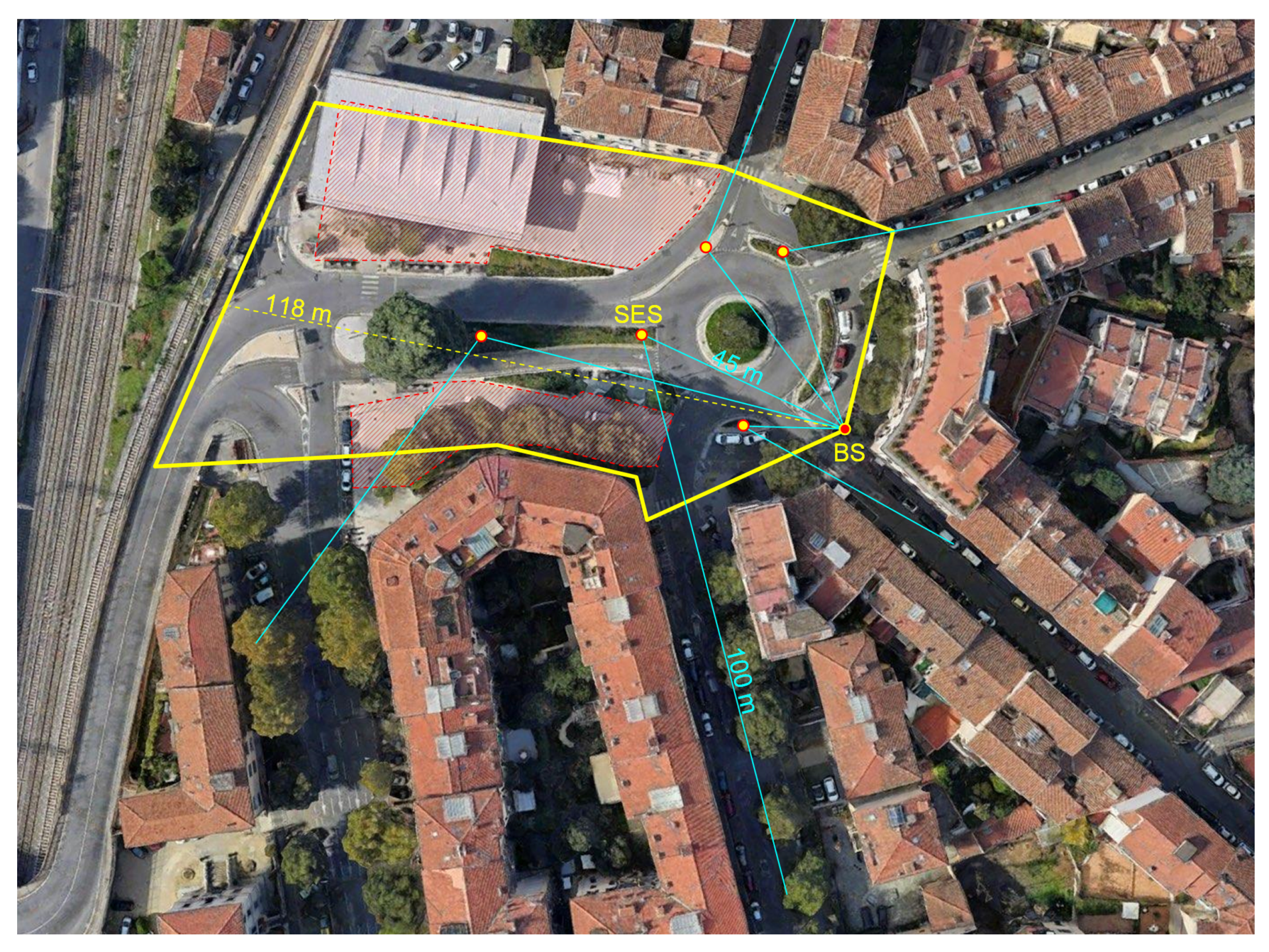
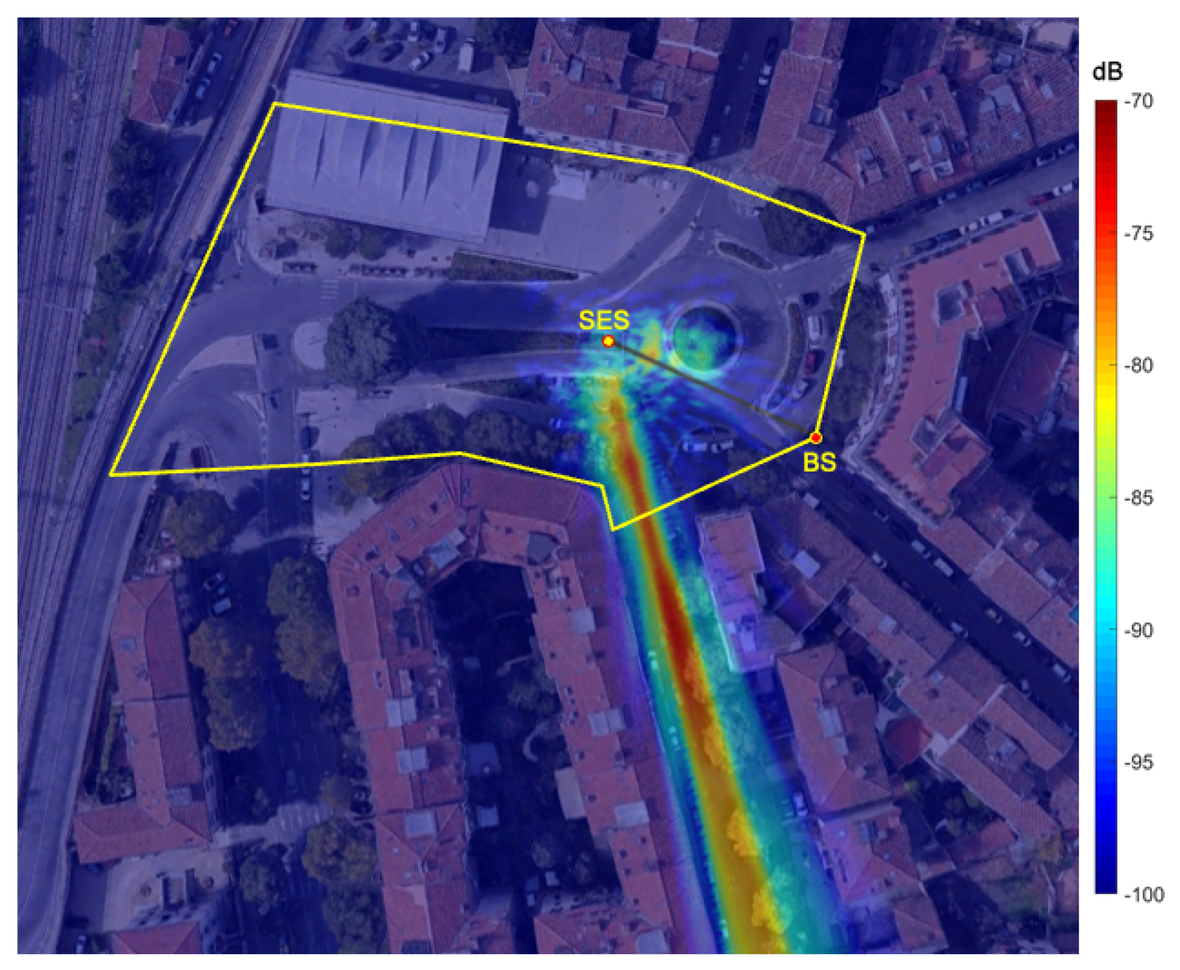
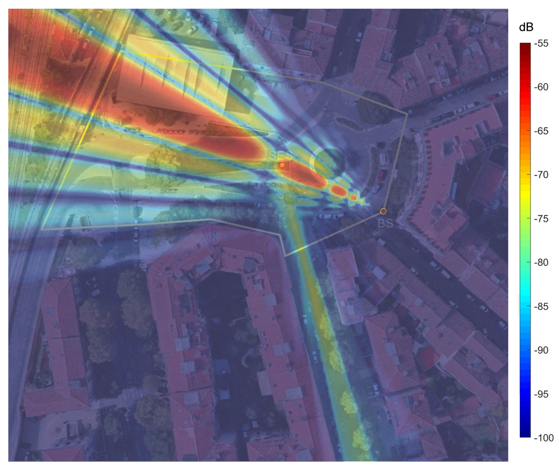
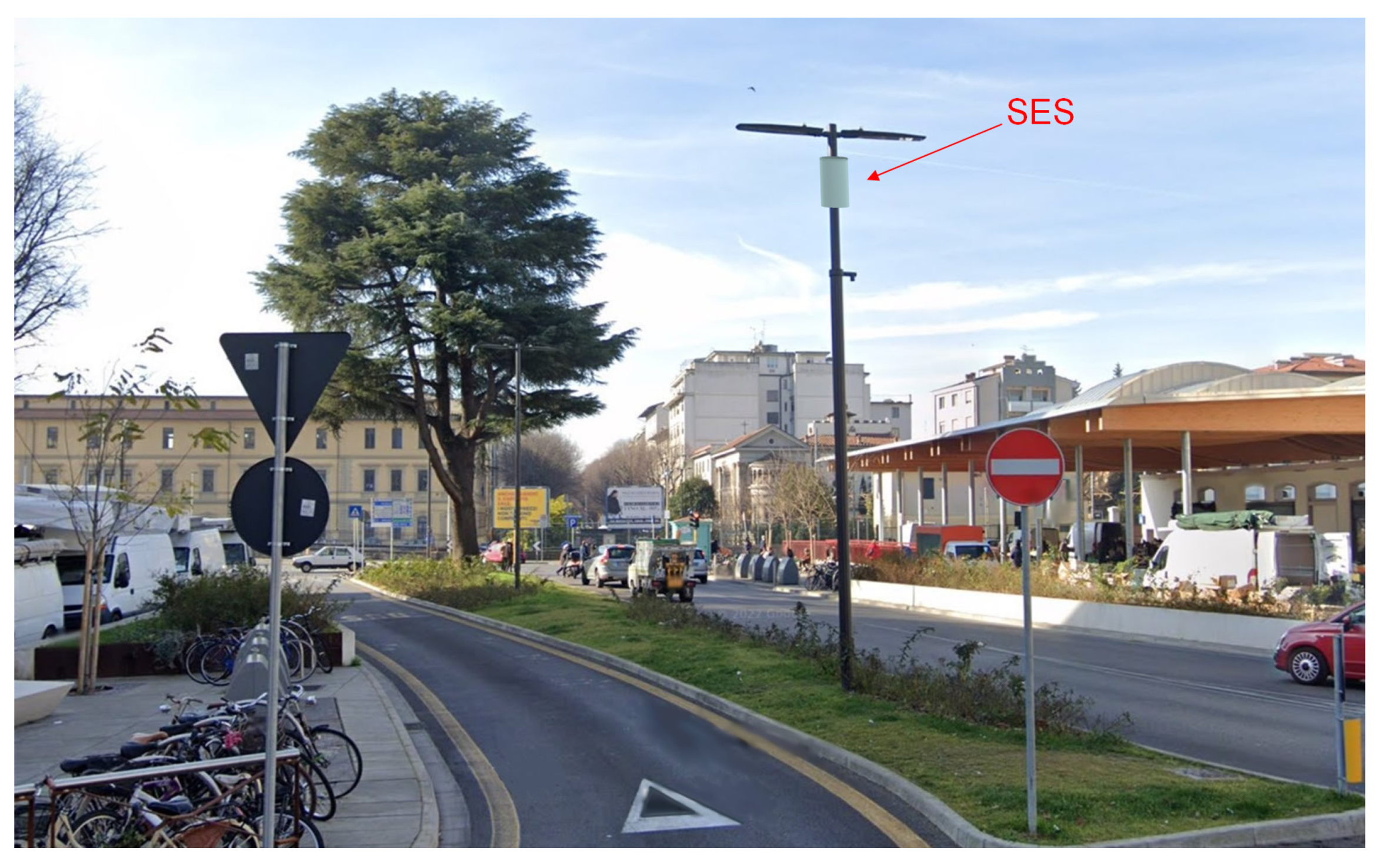
2. Scenario
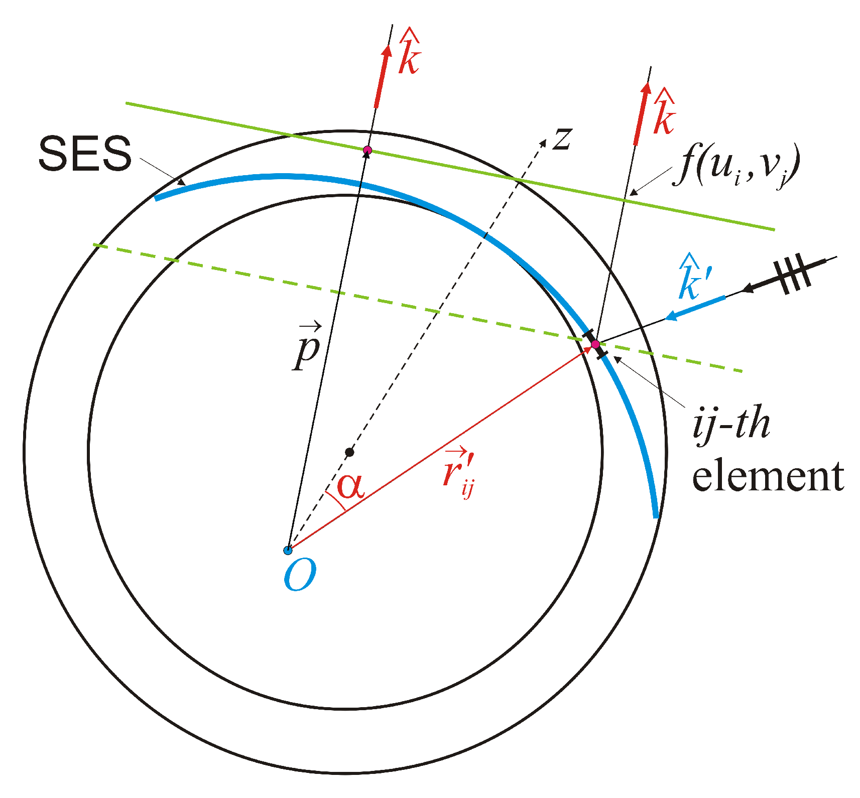
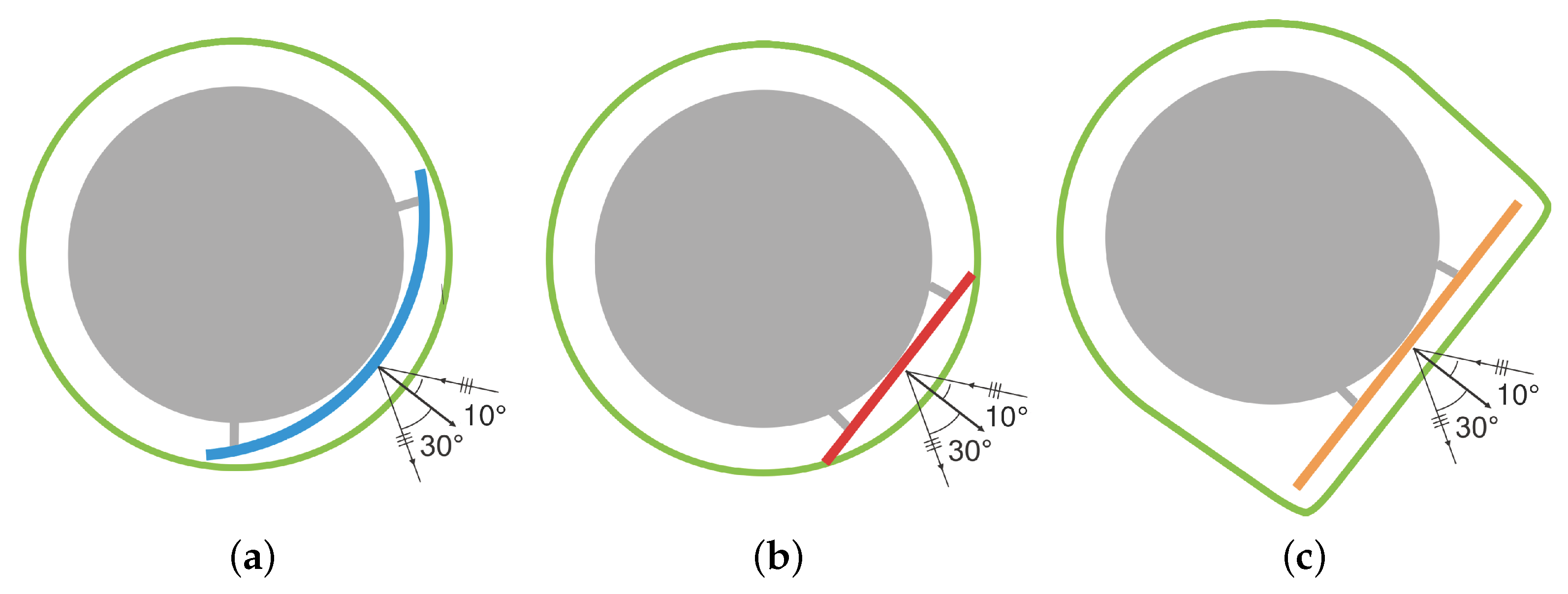
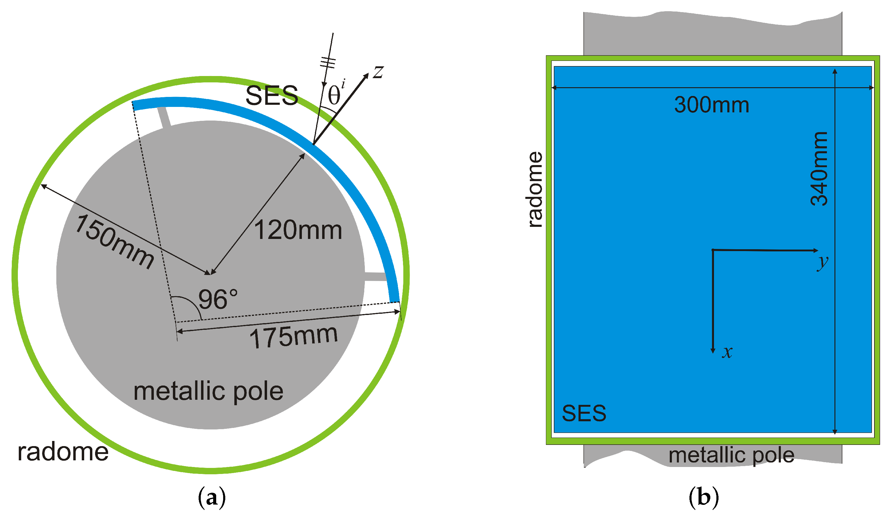
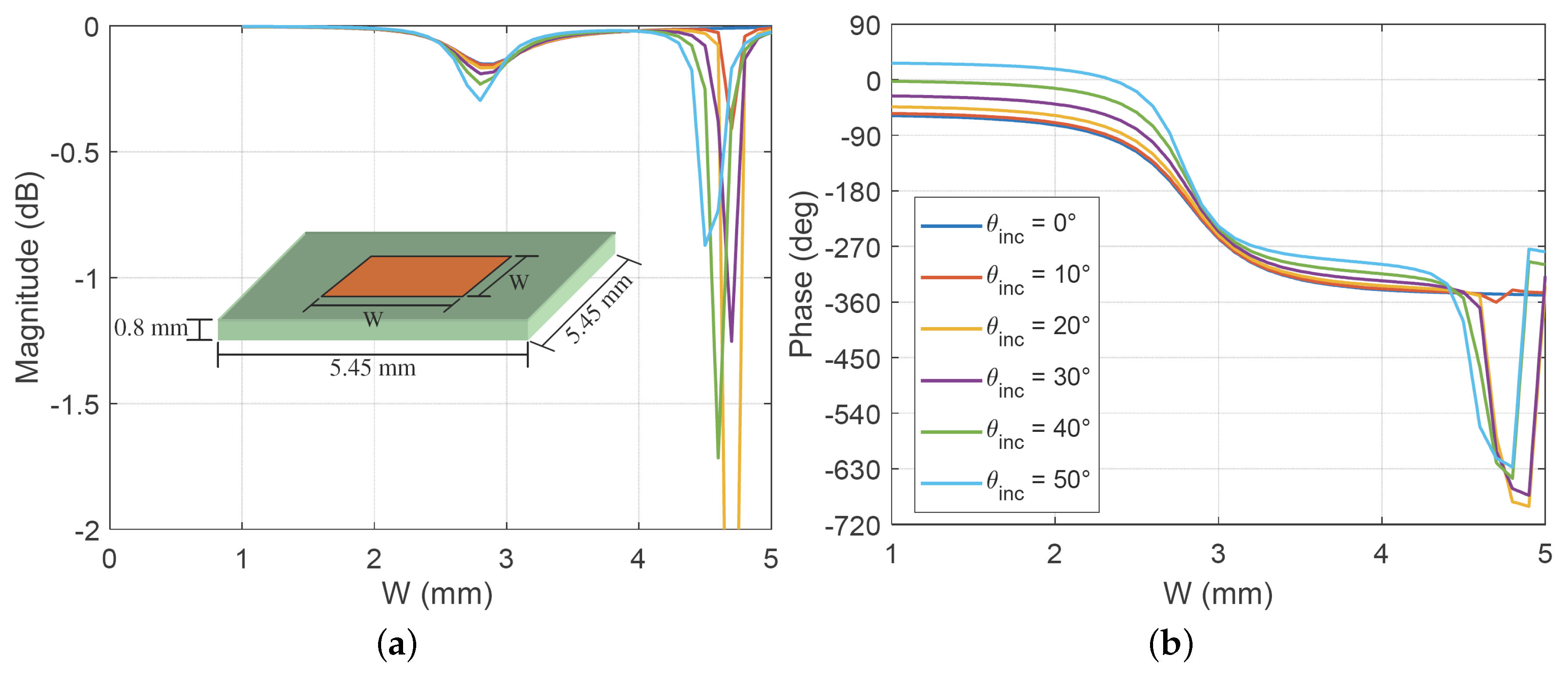
3. Design of a Curved SES
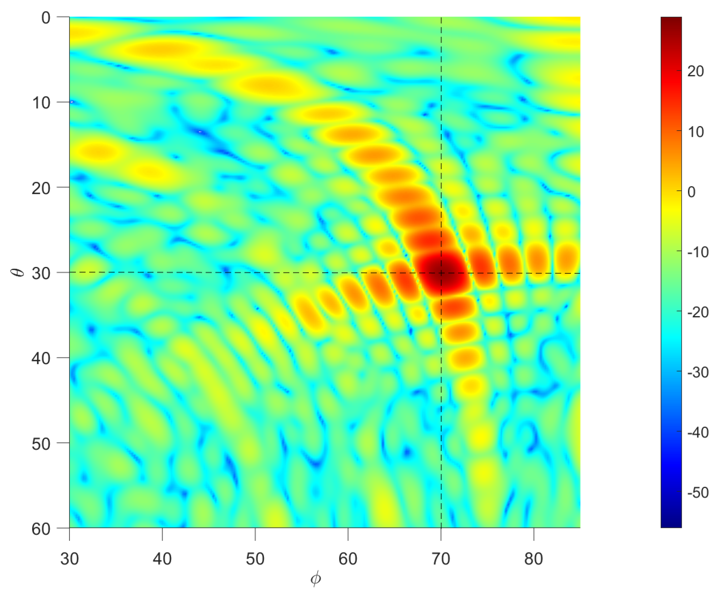
4. Results
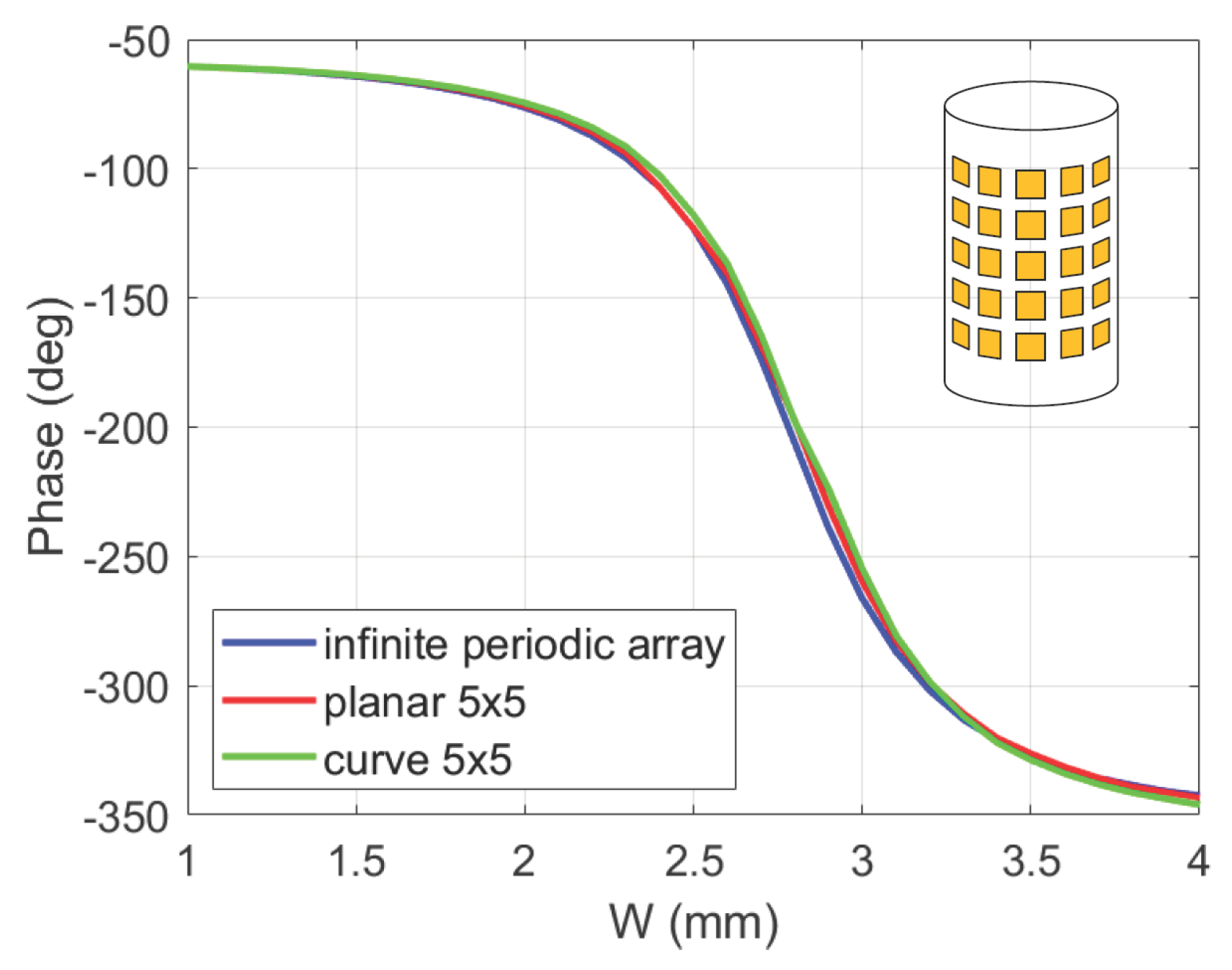
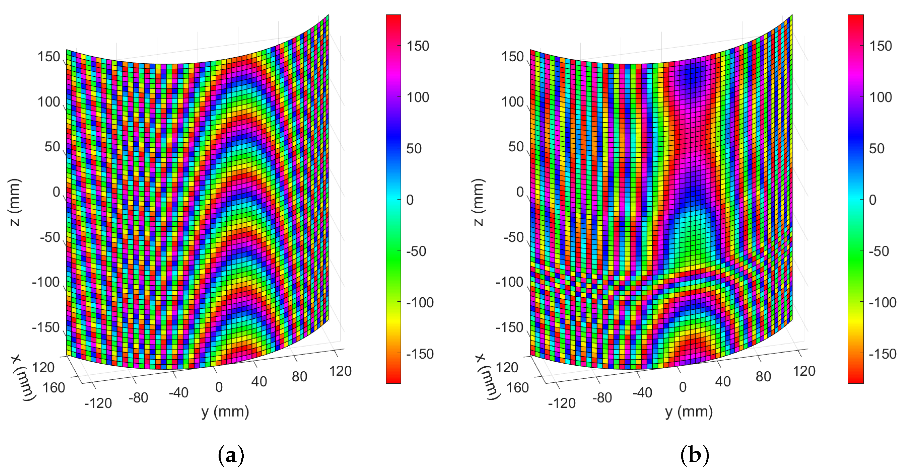
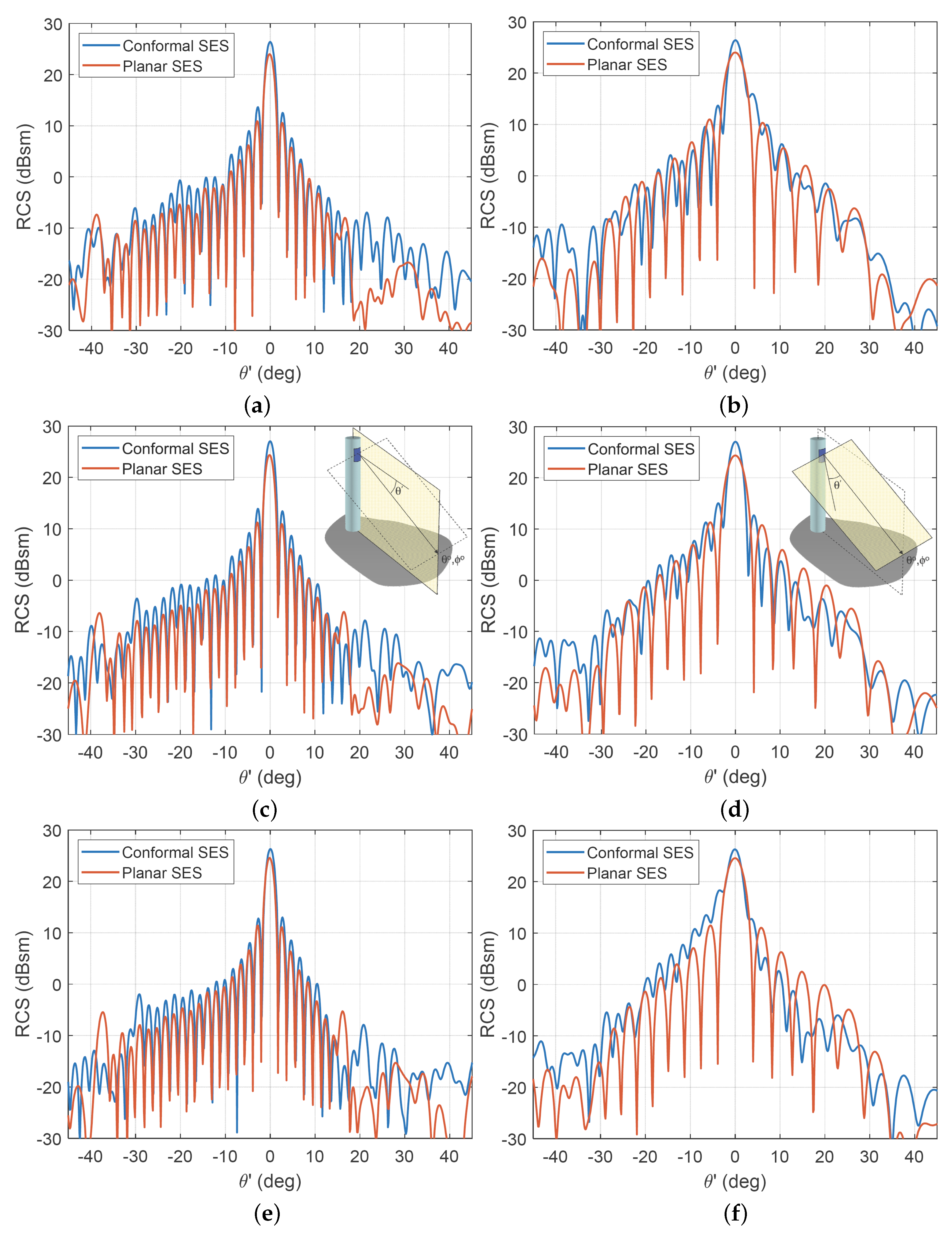
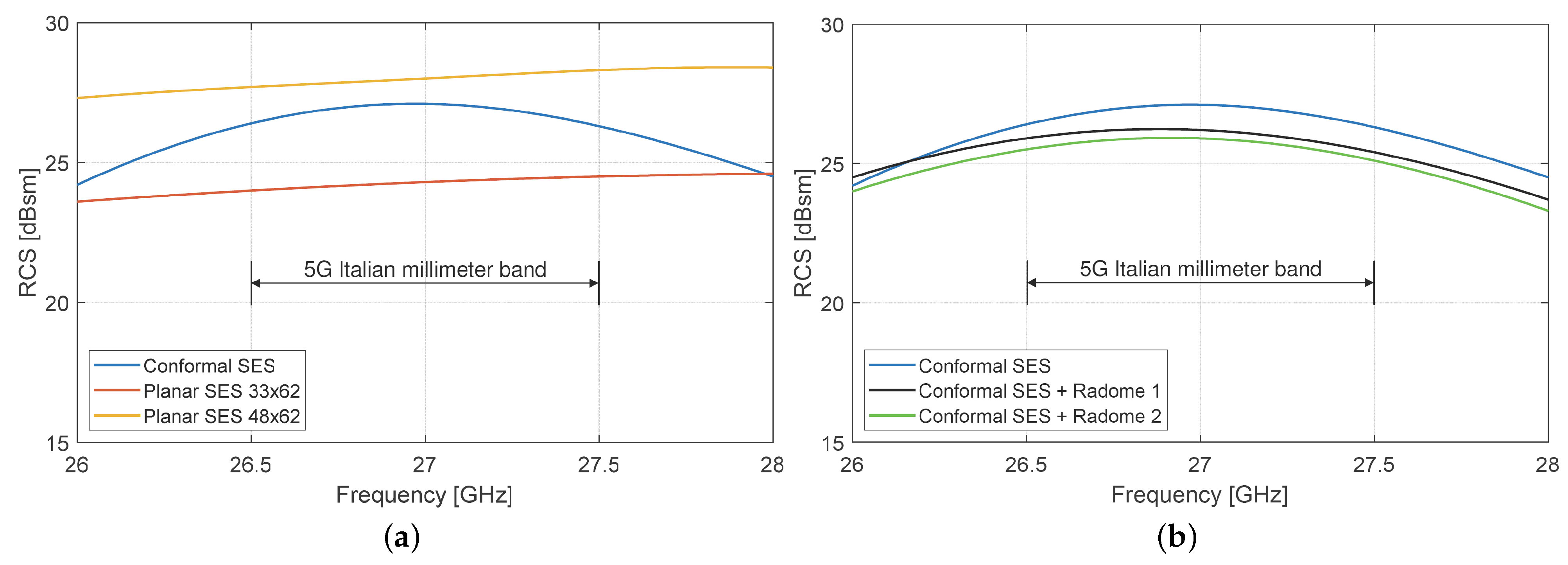
4.1. Comparison between Planar and Curved SES
4.2. Radome Influence
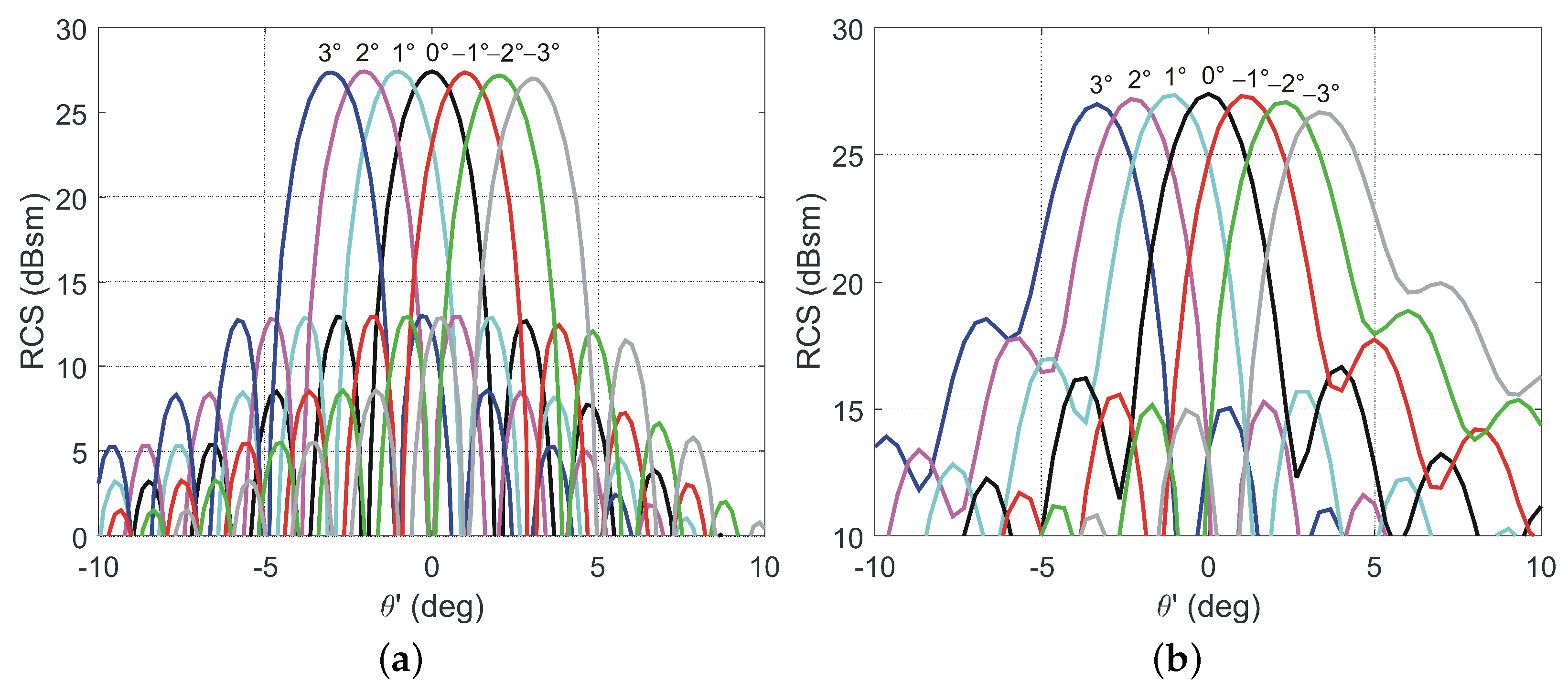
4.3. Incidence Sensitivity
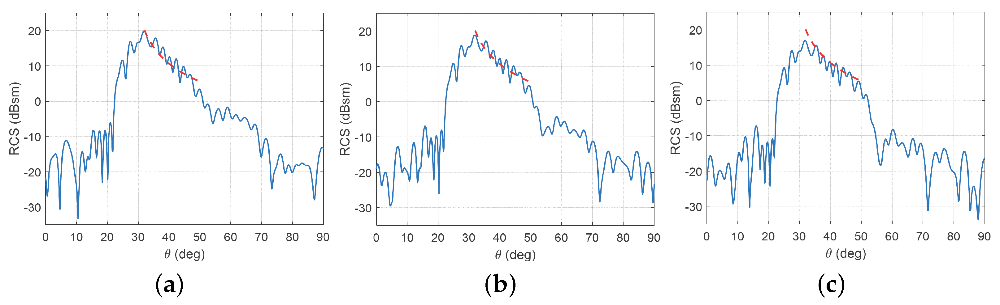
4.4. Example of Real Application
5. Conclusions
Author Contributions
Funding
Conflicts of Interest
Abbreviations
| SES | Smart Electromagnetic Skins |
| BS | Base Station |
| LOS | Line of Sight |
| RCS | Radar Cross Section |
References
- Tataria, H.; Shafi, M.; Molisch, A.F.; Dohler, M.; Sjöland, H.; Tufvesson, F. 6G Wireless Systems: Vision, Requirements, Challenges, Insights, and Opportunities. Proc. IEEE 2021, 109, 1166–1199. [Google Scholar] [CrossRef]
- Chowdhury, M.Z.; Shahjalal, M.; Ahmed, S.; Jang, Y.M. 6G Wireless Communication Systems: Applications, Requirements, Technologies, Challenges, and Research Directions. IEEE Open J. Commun. Soc. 2020, 1, 957–975. [Google Scholar] [CrossRef]
- Matthaiou, M.; Yurduseven, O.; Ngo, H.Q.; Morales-Jimenez, D.; Cotton, S.L.; Fusco, V.F. The Road to 6G: Ten Physical Layer Challenges for Communications Engineers. IEEE Commun. Mag. 2020, 59, 64–69. [Google Scholar] [CrossRef]
- Erricolo, D.; Rozhkova, A.; Stutts, A.C. Towards Smart Electromagnetic Environments. In Proceedings of the 2021 Computing, Communications, and IoT Applications (ComComAp), Shenzhen, China, 26–28 November 2021. [Google Scholar]
- Flamini, R.; De Donno, D.; Gambini, J.; Giuppi, F.; Mazzucco, C.; Milani, A.; Resteghini, L. Towards a Heterogeneous Smart Electromagnetic Environment for Millimeter-Wave Communications: An Industrial Viewpoint. IEEE Trans. Antennas Propag. 2022, 70, 8898–8910. [Google Scholar] [CrossRef]
- Liaskos, C.; Tsioliaridou, A.; Pitsillides, A.; Ioannidis, S.; Akyildiz, I. Using any surface to realize a new paradigm for wireless communications. Commun. ACM 2018, 61, 30–33. [Google Scholar] [CrossRef]
- Kamaruddin, N.A.; Mahmud, A.; Alias, M.Y.B.; Aziz, A.A.; Yaakob, S. Performance Evaluation of Reconfigurable Intelligent Surface against Distributed Antenna System at the Cell Edge. Electronics 2022, 11, 2376. [Google Scholar] [CrossRef]
- Massa, A.; Benoni, A.; Da Rù, P.; Goudos, S.K.; Li, B.; Oliveri, G.; Polo, A.; Rocca, P.; Salucci, M. Designing Smart Electromagnetic Environments for Next-Generation Wireless Communications. Telecom 2021, 2, 213–221. [Google Scholar] [CrossRef]
- Oliveri, G.; Zardi, F.; Rocca, P.; Salucci, M.; Massa, A. Building a Smart EM Environment-AI-Enhanced Aperiodic Micro-Scale Design of Passive EM Skins. IEEE Trans. Antennas Propag. 2022, 70, 8757–8770. [Google Scholar] [CrossRef]
- Oliveri, G.; Rocca, P.; Salucci, M.; Massa, A. Holographic Smart EM Skins for Advanced Beam Power Shaping in Next Generation Wireless Environments. IEEE J. Multiscale Multiph. Comp. Tech. 2021, 6, 171–182. [Google Scholar] [CrossRef]
- Rocca, P.; Da Rù, P.; Anselmi, N.; Salucci, M.; Oliveri, G.; Erricolo, D.; Massa, A. On the Design of Modular Reflecting EM Skins for Enhanced Urban Wireless Coverage. IEEE Trans. Antennas Propag. 2022, 70, 8771–8784. [Google Scholar] [CrossRef]
- Oliveri, G.; Zardi, F.; Rocca, P.; Salucci, M.; Massa, A. Constrained Design of Passive Static EM Skins. IEEE Trans. Antennas Propag. 2023, 71, 1528–1538. [Google Scholar] [CrossRef]
- Martinez-de-Rioja, E.; Vaquero, Á.F.; Arrebola, M.; Carrasco, E.; Encinar, J.A.; Achour, M. Passive intelligent reflecting surfaces based on reflectarray panels to enhance 5G millimeter-wave coverage. Int. J. Microw. Wirel. Tech. 2022, 15, 1–12. [Google Scholar] [CrossRef]
- Oliveri, G.; Salucci, M.; Massa, A. Generalized Analysis and Unified Design of EM Skins. IEEE Trans. Antennas Propag. 2023, 71, 6579–6592. [Google Scholar] [CrossRef]
- Oliveri, G.; Salucci, M.; Massa, A. Features and Potentialities of Static Passive EM Skins for NLOS Specular Wireless Links. IEEE Trans. Antennas Propag. 2023, 71, 8048–8060. [Google Scholar] [CrossRef]
- Benoni, A.; Capra, F.; Salucci, M.; Massa, A. Towards Real-World Indoor Smart Electromagnetic Environments—A Large-Scale Experimental Demonstration. IEEE Trans. Antennas Propag. 2023. early access. [Google Scholar] [CrossRef]
- Basar, E.; Renzo, M.D.; Rosny, J.D.; Debbah, M.; Alouini, M.-S.; Zhang, R. Wireless Communications Through Reconfigurable Intelligent Surfaces. IEEE Access 2019, 7, 116753–116773. [Google Scholar] [CrossRef]
- Di Renzo, M.; Zappone, A.; Debbah, M.; Alouini, M.S.; Yuen, C.; De Rosny, J.; Tretyakov, S. Smart Radio Environments Empowered by Reconfigurable Intelligent Surfaces: How It Works, State of Research, and the Road Ahead. IEEE J. Sel. Areas Comm. 2020, 38, 2450–2525. [Google Scholar] [CrossRef]
- Wu, Q.; Zhang, S.; Zheng, B.; You, C.; Zhang, R. Intelligent Reflecting Surface-Aided Wireless Communications: A Tutorial. IEEE Trans. Commun. 2021, 69, 3313–3351. [Google Scholar] [CrossRef]
- Zhao, J. A Survey of Intelligent Reflecting Surfaces (IRSs): Towards 6G Wireless Communication Networks. arXiv 2019, arXiv:1907.04789. [Google Scholar]
- Yurduseven, O.; Assimonis, S.D.; Matthaiou, M. Intelligent Reflecting Surfaces with Spatial Modulation: An Electromagnetic Perspective. IEEE Open J. Comm. Soc. 2020, 1, 1256–1266. [Google Scholar] [CrossRef]
- Pitilakis, A.; Tsilipakos, O.; Liu, F.; Kossifos, K.M.; Tasolamprou, A.C.; Kwon, D.H.; Mirmoosa, M.S.; Manessis, D.; Kantartzis, N.V.; Liaskos, C.; et al. A Multi-Functional Reconfigurable Metasurface: Electromagnetic Design Accounting for Fabrication Aspects. IEEE Trans. Antennas Propag. 2021, 69, 1440–1454. [Google Scholar] [CrossRef]
- Pérez-Adán, D.; Fresnedo, Ó.; González-Coma, J.P.; Castedo, L. Intelligent Reflective Surfaces for Wireless Networks: An Overview of Applications, Approached Issues, and Open Problems. Electronics 2021, 10, 2345. [Google Scholar] [CrossRef]
- Liu, Y.; Liu, X.; Mu, X.; Hou, T.; Xu, J.; Di Renzo, M.; Al-Dhahir, N. Reconfigurable Intelligent Surfaces: Principles and Opportunities. IEEE Comm. Surv. Tutorials 2021, 23, 1546–1577. [Google Scholar] [CrossRef]
- Mei, P.; Cai, Y.; Zhao, K.; Ying, Z.; Pedersen, G.F.; Lin, X.Q.; Zhang, S. On the Study of Reconfigurable Intelligent Surfaces in the Near-Field Region. IEEE Trans. Antennas Propag. 2022, 70, 8718–8728. [Google Scholar] [CrossRef]
- Dash, S.; Psomas, C.; Krikidis, I.; Akyildiz, I.F.; Pitsillides, A. Active Control of THz Waves in Wireless Environments using Graphene-based RIS. IEEE Trans. Antennas Propag. 2022, 70, 8785–8797. [Google Scholar] [CrossRef]
- Degli-Esposti, V.; Vitucci, E.M.; Renzo, M.D.; Tretyakov, S. Reradiation and Scattering from a Reconfigurable Intelligent Surface: A General Macroscopic Model. IEEE Trans. Antennas Propag. 2022, 70, 8691–8706. [Google Scholar] [CrossRef]
- Sharma, T.; Chehri, A.; Fortier, P. Reconfigurable Intelligent Surfaces for 5G and beyond Wireless Communications: A Comprehensive Survey. Energies 2021, 14, 8219. [Google Scholar] [CrossRef]
- Demmer, D.; Foglia Manzillo, F.; Gharbieh, S.; Śmierzchalski, M.; D’Errico, R.; Doré, J.B.; Clemente, A. Hybrid Precoding Applied to Multi-Beam Transmitting Reconfigurable Intelligent Surfaces (T-RIS). Electronics 2023, 13, 1162. [Google Scholar] [CrossRef]
- Liu, Y.; Dou, J.; Cui, Y.; Chen, Y.; Yang, J.; Qin, F.; Wang, Y. Reconfigurable Intelligent Surface Physical Model in Channel Modeling. Electronics 2022, 11, 2798. [Google Scholar] [CrossRef]
- Vitucci, E.M.; Fabiani, M.; Degli-Esposti, V. Use of a Realistic Ray-Based Model for the Evaluation of Indoor RF Coverage Solutions Using Reconfigurable Intelligent Surfaces. Electronics 2023, 12, 1173. [Google Scholar] [CrossRef]
- Dai, L.; Wang, B.; Wang, M.; Yang, X.; Tan, J.; Bi, S.; Xu, S.; Yang, F.; Chen, Z.; Di Renzo, M.; et al. Reconfigurable intelligent surface-based wireless communications: Antenna design, prototyping, and experimental results. IEEE Access 2020, 8, 45913–45923. [Google Scholar] [CrossRef]
- Oliveri, G.; Rocca, P.; Salucci, M.; Erricolo, D.; Massa, A. Multi-Scale Single-Bit RP-EMS Synthesis for Advanced Propagation Manipulation Through System-by-Design. IEEE Trans. Antennas Propag. 2022, 10, 8809–8824. [Google Scholar] [CrossRef]
- Vaquero, A.F.; Martinez-de-Rioja, E.; Arrebola, M.; Encinar, J.A. Study on the Effect of the Wall in the Performance of an Intelligent Reflective Surface for Providing Coverage in mm-Wave Frequencies. In Proceedings of the European Conference on Antennas and Propag. (EuCAP), Florence, Italy, 26–31 March 2023. [Google Scholar]
- Future Access 28 Ghz Phased Array Antenna Module (PAAM). 2023. Available online: https://mmwavetech.fujikura.jp/5g/ (accessed on 31 October 2023).
- CST Microwave Studio. 2023. Available online: http://www.cst.com/ (accessed on 31 October 2023).
- Balanis, C.A. Antenna Theory Analysis and Design, 3rd ed.; Equation (2-120a); Wiley-Interscience a John Wiley & Sons, Inc.: Hoboken, NJ, USA, 2005. [Google Scholar]
- Buckley, M.J. Synthesis of Shaped Beam Antenna Pattern Using Implicit Constrained Current Elements. IEEE Trans. Antennas Propag. 1996, 44, 192–197. [Google Scholar] [CrossRef]


Disclaimer/Publisher’s Note: The statements, opinions and data contained in all publications are solely those of the individual author(s) and contributor(s) and not of MDPI and/or the editor(s). MDPI and/or the editor(s) disclaim responsibility for any injury to people or property resulting from any ideas, methods, instructions or products referred to in the content. |
© 2023 by the authors. Licensee MDPI, Basel, Switzerland. This article is an open access article distributed under the terms and conditions of the Creative Commons Attribution (CC BY) license (https://creativecommons.org/licenses/by/4.0/).
Share and Cite
Freni, A.; Beccaria, M.; Mazzinghi, A.; Massaccesi, A.; Pirinoli, P. Low-Profile and Low-Visual Impact Smart Electromagnetic Curved Passive Skins for Enhancing Connectivity in Urban Scenarios. Electronics 2023, 12, 4491. https://doi.org/10.3390/electronics12214491
Freni A, Beccaria M, Mazzinghi A, Massaccesi A, Pirinoli P. Low-Profile and Low-Visual Impact Smart Electromagnetic Curved Passive Skins for Enhancing Connectivity in Urban Scenarios. Electronics. 2023; 12(21):4491. https://doi.org/10.3390/electronics12214491
Chicago/Turabian StyleFreni, Angelo, Michele Beccaria, Agnese Mazzinghi, Andrea Massaccesi, and Paola Pirinoli. 2023. "Low-Profile and Low-Visual Impact Smart Electromagnetic Curved Passive Skins for Enhancing Connectivity in Urban Scenarios" Electronics 12, no. 21: 4491. https://doi.org/10.3390/electronics12214491
APA StyleFreni, A., Beccaria, M., Mazzinghi, A., Massaccesi, A., & Pirinoli, P. (2023). Low-Profile and Low-Visual Impact Smart Electromagnetic Curved Passive Skins for Enhancing Connectivity in Urban Scenarios. Electronics, 12(21), 4491. https://doi.org/10.3390/electronics12214491