Review

A Survey of Ultra-Low-Power Amplifiers for Internet of Things Nodes

Department of Electrical, Electronic and Computer Engineering, University of Catania, Viale A. Doria 6, 95125 Catania, Italy
*
Authors to whom correspondence should be addressed.
Electronics 2023, 12(20), 4361; https://doi.org/10.3390/electronics12204361
Submission received: 7 September 2023 / Revised: 12 October 2023 / Accepted: 18 October 2023 / Published: 20 October 2023
(This article belongs to the Special Issue Feature Papers in Circuit and Signal Processing)

Abstract

:
This paper investigates CMOS operational transconductance amplifier (OTA) design methodologies suitable for Internet of Things nodes. The use of MOS transistors in the subthreshold of the body terminal for signal input or bias, as well as newer inverter- and digital-based techniques, is considered. Solutions from the authors’ work are utilized as main case examples. State-of-the-art ultra-low-power OTAs are then thoroughly compared using a data-driven approach. According to the findings, digital- and inverter-based solutions have the lowest area occupation and superior small-signal performance but are inherently susceptible to process, supply, and temperature (PVT) variations. The only “analog” approach suitable for a sub-0.6 V supply is body driving in conjunction with subthreshold bias. It offers competitive large-signal performance and, more importantly, is less sensitive to PVT variations at the expense of silicon area.

1. Introduction

The Internet of Things (IoT) has wide-ranging potential applications with expected significant impacts across various industries, including agriculture, healthcare, automotive, and industrial manufacturing. A conservative projection estimates that the number of interconnected IoT devices will reach approximately 29 billion by 2030 from 9.7 billion in 2020, indicating a substantial growth in the use of this technology in the coming years [1].
Among the most important characteristics of IoT nodes are computing, wireless communication, and sensor capabilities [2]. Indeed, IoT node implementation requires circuits that connect the digital processing domain with physical signals received from the analog world via sensors such as temperature, CO2, light, humidity, displacement, pressure, and acceleration. As a result, analog interfaces are critical elements in the IoT paradigm [3] because IoT nodes are commonly wireless and energy-autonomous and hence have a very limited power budget that often relies on small primary batteries or area-constrained energy harvesters, with the optional support of secondary batteries. As a result, there is an urgent need to heavily reduce the power consumption of digital cores and analog frontends, and, for this purpose, efficient IoT nodes must exploit ultra-low-voltage design techniques with an operating voltage of 1 V or less. Furthermore, the utilization of sub-100 nm CMOS technologies is required to improve the power-delay product of digital circuits, which constitute the bulk of an IoT device [2]. However, the scaling of CMOS technology, the low supply voltage available, and the limited allowed power consumption lead to deleterious effects in the analog domain, such as a drop in output resistance, dynamic range, and signal-to-noise ratio. Consequently, designing the analog front end becomes a challenging task that can seriously impact the overall IoT node performance [4].
In this framework, the operational transconductance amplifier (OTA) is one of the fundamental building blocks of the analog front end. Various design techniques are today available to enable efficient OTA performance at low power, including weak inversion (or subthreshold) operation [5,6,7,8,9,10,11], bulk-driving (or body-driving) [12,13,14,15,16,17,18,19,20,21,22,23,24,25,26,27,28,29,30], body-biasing [31,32,33], inverter-based [34,35,36,37,38,39,40,41,42,43], and fully digital approaches [44,45,46,47,48,49,50,51]. Floating-gate and quasi-floating-gate techniques can also be mentioned [52,53]. However, the latter ones employ custom transistors that are not included in commercial design kits. In addition, the temperature dependence of the pseudo-resistor adopted (not adequately modeled in CAD tools) limits the use of this approach. Furthermore, a relevant limitation is leakage currents, which can make this technique unfeasible in sub-100 nm CMOS processes. As a result, we will not investigate floating-gate and quasi-floating-gate transistor solutions by limiting our analysis to techniques appropriate for conventional CMOS technologies and acceptable by the industry standards.
The aim of this paper is hence to review the main design techniques suitable for ultra-low-power, ultra-low-voltage OTAs, highlighting their advantages and trade-offs. In this field, the authors have decades of expertise and have devised several solutions, some of which will be discussed in the next sections and will be chosen as design examples. A data-driven analysis of the state of the art is also performed to offer the designer some guidance for selecting the best OTA solution based on the specified design parameters and system needs.
The paper is organized as follows. Section 2, Section 3, Section 4, Section 5 and Section 6 provide a succinct examination of the working principles of the CMOS subthreshold, body-driving, body-biasing, inverter-based, and digital techniques, as well as selected example designs. Section 7 compares the key solutions acquired from the state of the art and that exploit the preceding methodologies. A quantitative, data-driven comparison is performed by considering the primary performance parameters and evaluating specific figures of merit often used in the literature. Section 8 summarizes the authors’ conclusions.

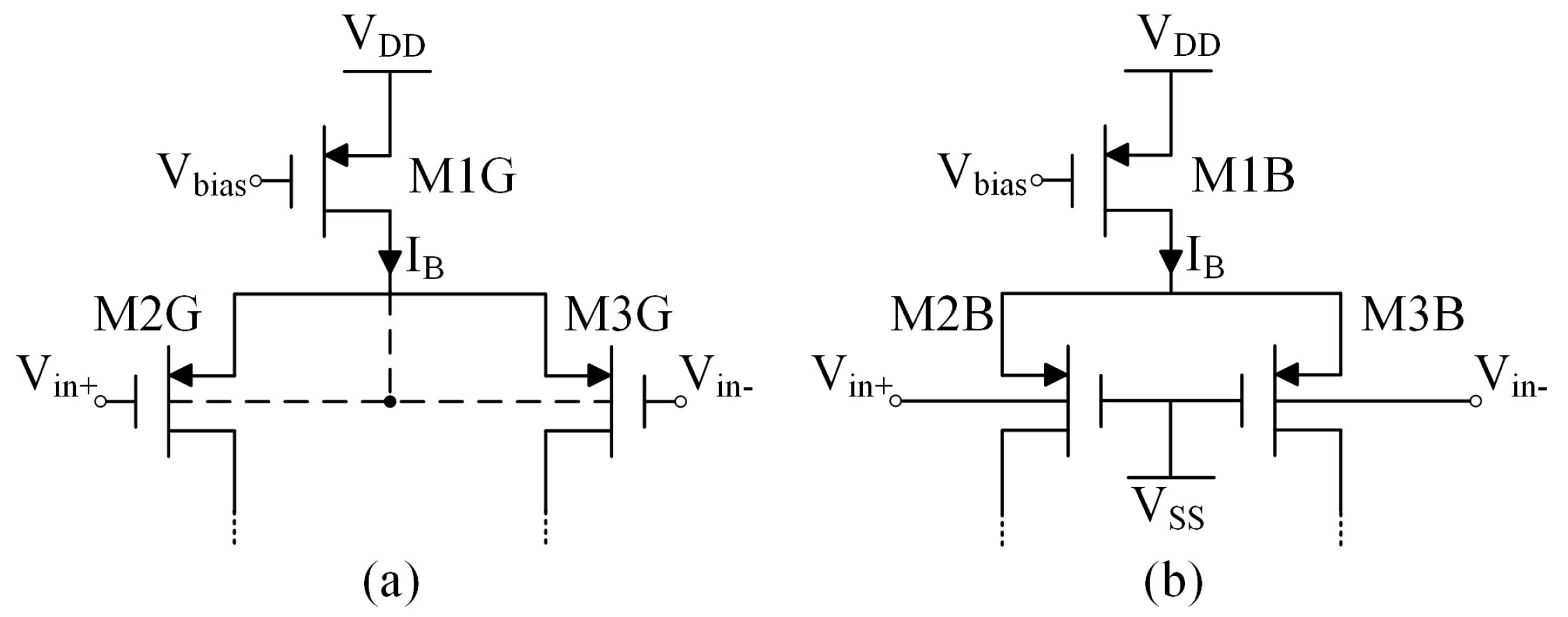
2. Subthreshold Approach

Operating transistors in the weak inversion (or subthreshold, SUB) region has been the primary technique for low-voltage and low-power analog design in MOS technology since the 1970s [5].
It is worth noting that in the subthreshold, the saturation condition is reached when V D S 4   V T , where VT is the thermal voltage. In this region, an exponential behavior between the drain current and the gate-source voltage is found. The second column of Table 1 shows the small-signal parameters of a gate-driven n-MOS transistor operating in the subthreshold region and in saturation. A bipolar-like behavior is apparent from the linear dependence of the transconductance gm on the drain current ID (1a). Subthreshold devices also show the highest transconductance efficiency (gm/ID) [4], while the intrinsic voltage gain, Av, = gm/gds, is equal to the reciprocal of nλVT (which is strictly related to the channel length), resulting in a minimization of distortion [6].
The main drawback of the approach is a larger drain current error between two otherwise ideally matched transistors, which, in the implementation of an OTA, tends to increase the offset and noise and to reduce the common-mode rejection ratio, CMRR.
Overcoming this issue may result in a complex design [54]. Moreover, since subthreshold operation implies very low standby currents, the reduced transconductance leads to limited bandwidth (4a), which is only partially compensated by the lower MOS parasitic capacitances provided by the scaled technologies. However, this is not a main issue because most of the sensor node applications, such as monitoring pressure, temperature, humidity, acceleration, or bio-signals, usually involve frequencies around the kilohertz [3]. For these reasons, the subthreshold region is popular in the implementation of analog building blocks, including OTAs supplied from 1 V under very limited current budgets [7,8,9,10,11,15].
As an example, a solution operating at 1 V and proposed in [11] is shown in Figure 1. The OTA clearly illustrates that conventional circuit configurations are employed. In this case, we have a folded-cascode differential stage M1–M8, followed by a common-source stage M9–M10, and as a final non-inverting stage, a common-source M11 transistor with a current mirror-load M12–M13. The subthreshold biasing point of the transistors here is the key aspect, and, in addition, the use of three gain stages is to compensate for the diminished intrinsic stage gain. Nested Miller frequency compensation capacitors C1 and C2 provide closed-loop stability.
The DC gain and the gain–bandwidth product (GBW) are
A = g m 1 , 2 g m 9 g m 11 r o 1 r o 2 r o 3
G B W = g m 1 , 2 C 1
where roi is the equivalent small-signal resistance at the output of the i-th stage (ro1rd8, ro2 = rd9//rd10, and ro3 = rd13//rd14). The DC gain is found to be greater than 120 dB, and the GBW is 20 kHz. The solution allows the driving of high capacitive loads up to 200 pF, with only 170 nA of standby current.

3. Body-Driven Approach

Traditional gate-driven approaches, either above or below the threshold, control the conductivity of the channel and, consequently, the drain current, ID, via the gate-source voltage. In contrast, in the bulk- or body-driven (BD) approach, ID is controlled by the bulk-source voltage, VBS. Figure 2a,b shows two different ways to implement a p-channel differential pair, one through the usual gate-driven approach and the other through the alternative bulk-driven approach. In the latter case, the differential input signal is applied to the bulk terminals of the transistors couple M2B–M3B, while the gate terminals are kept to a reference voltage (VSS in this case) [17].
Removing the limitation given by the threshold voltage associated with the gate terminal, the input common-mode range of the BD pair is maximized, since the input voltages can span from VSS to VDD. The main advantage of this approach is, indeed, the ability to achieve rail-to-rail input operation under supply voltages comparable to or even less than the threshold voltage. It is, of course, mandatory that the bulk-source junction is not turned on. Otherwise, the bulk source junction starts to draw a non-negligible current. For rail-to-rail operation, the approach is hence particularly profitable for supplies (VDD–VSS) below 0.5 V, just below the junction threshold.
Returning to Figure 2b, we observe that the gates of M2B–M3B, connected to VSS, can be instead used to set the standby current of M2B–M3B through a conventional current mirror and by eliminating the tail current generator M1B. In this manner supply demand is further reduced at the cost of a lower power supply rejection ratio, PSRR [55]. It is also noteworthy that the BD approach requires the use of a triple-well technology if the body terminal of both p- and n-channel MOS devices must be exploited. As a drawback, this results in greater area occupation.
The third column of Table 1 shows the small-signal parameters of a body-driven transistor operating in saturation above the threshold region. Since the bulk transconductance gmb is only about 10% to 20% of gm, as highlighted by (2b), bulk-driven configurations are characterized by reduced values of the intrinsic gain Av and transition frequency fT.
Several bulk-driven OTAs have been proposed in literature [12,14,15,16,17,18,19,20,21,22,23,24,25,26,27,28,29,30]. Most of these solutions also operate transistors in the subthreshold to minimize the supply voltage requirements. Moreover, multistage architectures are often utilized to overcome the lower value of the DC gain. Positive feedback is also exploited to increase both the input transconductance and the gain–bandwidth product. To give an example, the schematic of the OTA proposed in [29] is shown in Figure 3. The resulting differential gain and gain–bandwidth product can be expressed as follows:
A = β 1 α g m b 1 , 2 r o
G B W = β 1 α g m b 1 , 2 C L
where the effect of the positive feedback is displayed by factor (1 − a) at the denominator. Of course, parameter a must be close but lower than 1 to preserve stability. With a = 0.83, and b= 15, we obtain a DC gain slightly lower than 40 dB and a GBW equal to 5 kHz, with a power consumption of around 32 nW. It is noteworthy that because of the absence of the tail current generator, M1–M2 is a pseudo-differential pair, but thanks to the action of M7 and M8, the whole OTA provides a quasi-differential behavior, as shown in [29].
For the same purpose of increasing input transconductance, the combination of the body-driven and AC-coupled gate-driven approaches has also been proposed in [56]. As it was already stated, this solution is not considered in this discussion due to the QFG technique limitation in the CMOS process.

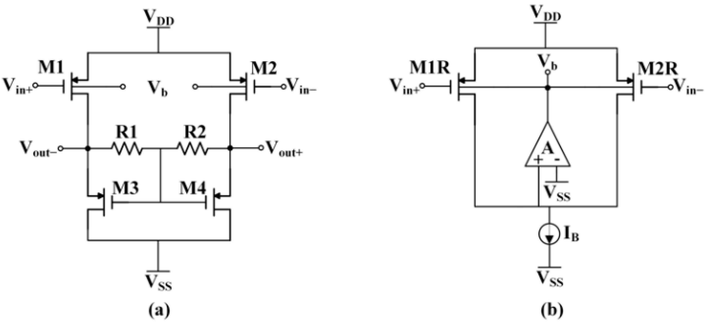
4. Body-Biased Approach

The body-biased (BB) approach is aimed at overcoming the limitations of the CMOS technology and/or of the conventional OTA topologies through threshold lowering [8,14], level shifting [16], body-driven gain boosting [19], and non-tailed differential pairs [33,55]. These techniques can also be combined together.
The body-biased approach followed in [31] exploits a gate-driven differential pair, thus providing a high gate transconductance, but (1) the tail current source is eliminated, leaving extra room for the input swing; additionally, (2) the body terminals of the pair are used both to control the common-mode (and hence also the DC) current and to reduce the threshold voltage through the body effect. Figure 4a,b, shows, respectively, the minimum-supply gate-driven differential pair and the simplified schematic of the common-mode control circuit. The common-mode control voltage Vb is generated in the circuit of Figure 4b, forcing IB/2 to flow in M1R (M2R) when Vin+ = Vin− = Vicm. Then, Vb is applied to the main circuit of Figure 4a. It is apparent that the quiescent (and common-mode) current in M1–M2 is mirrored from that of M1R–M2R, and hence, M1–M2 acts as a differential pair but without the tail current source. Moreover, under suitable values of W/L)1R2R and IB, the voltage Vb is less than VDD, and the threshold voltage of M1R–M2R is diminished.
The gain of the circuit in Figure 4a can be expressed as
A g m 1 , 2 2 R 1 , 2
where the output resistance of transistors is neglected.
Based on this approach, an optimized solution that provides relatively low noise around 65 nV/ H z and a total current consumption of 27 µA with a good trade-off between DC gain (65 dB) and gain–bandwidth product (1 MHz) has been experimentally validated in [33].

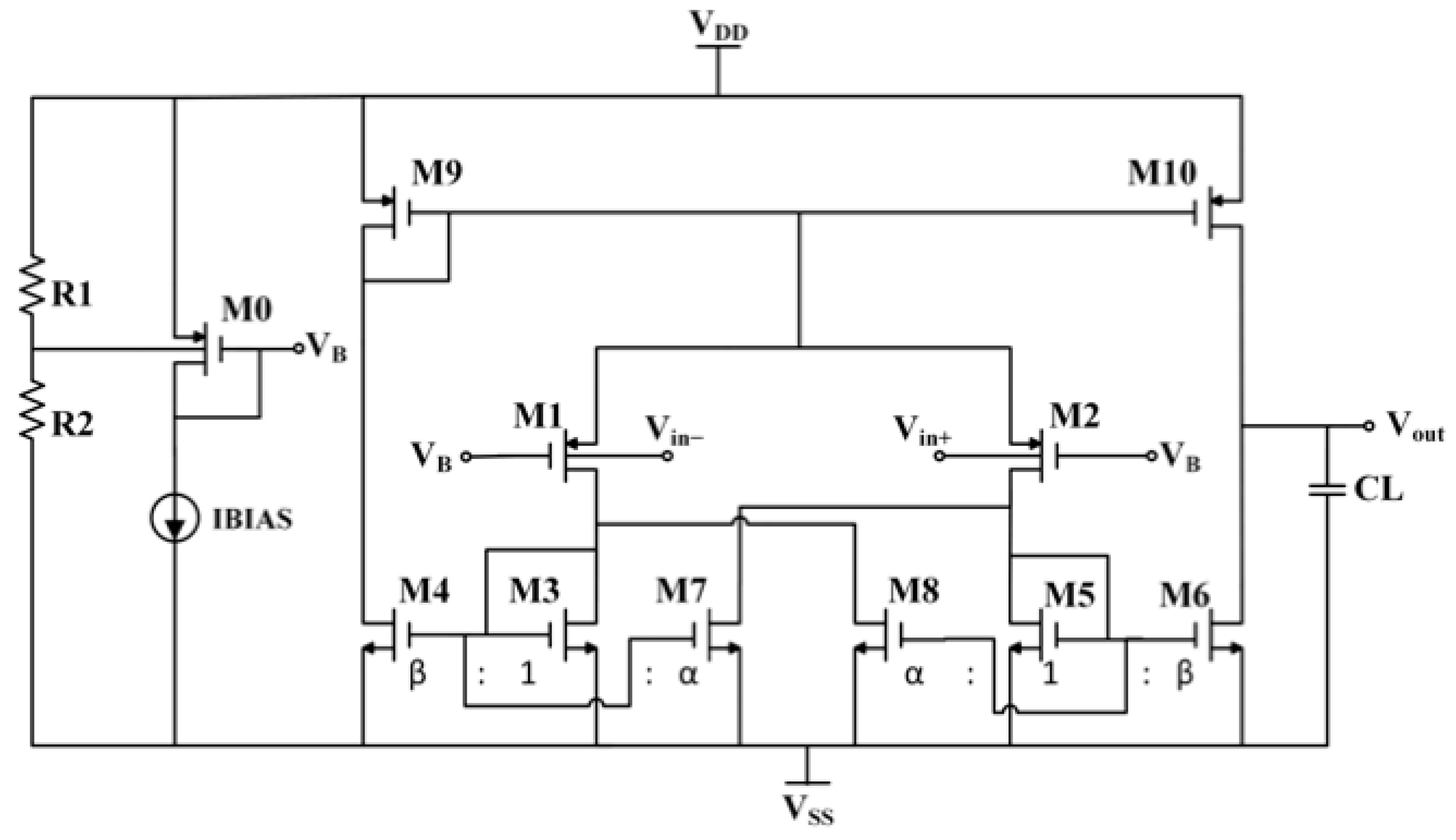
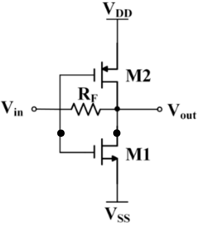
5. Inverter-Based Approach
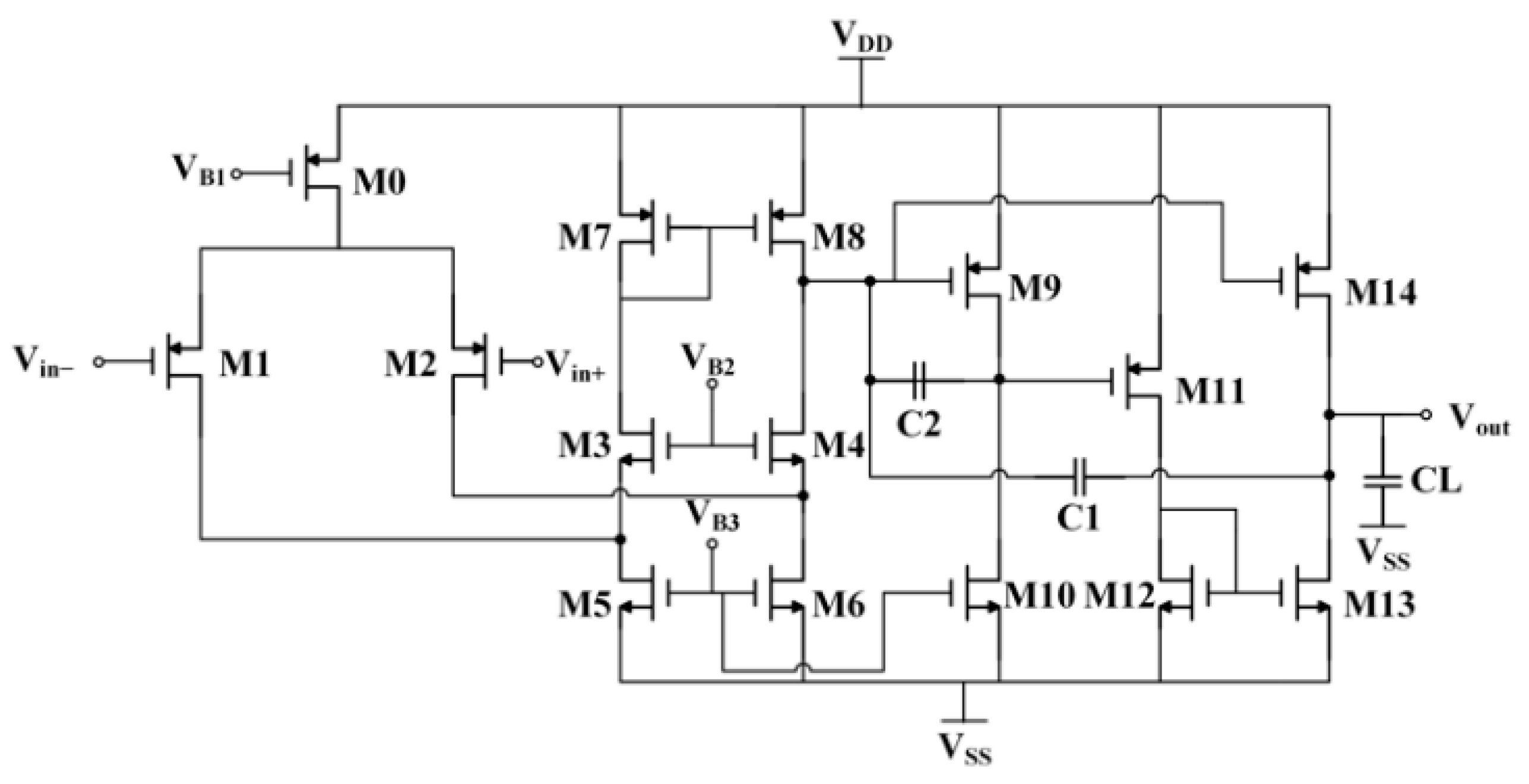
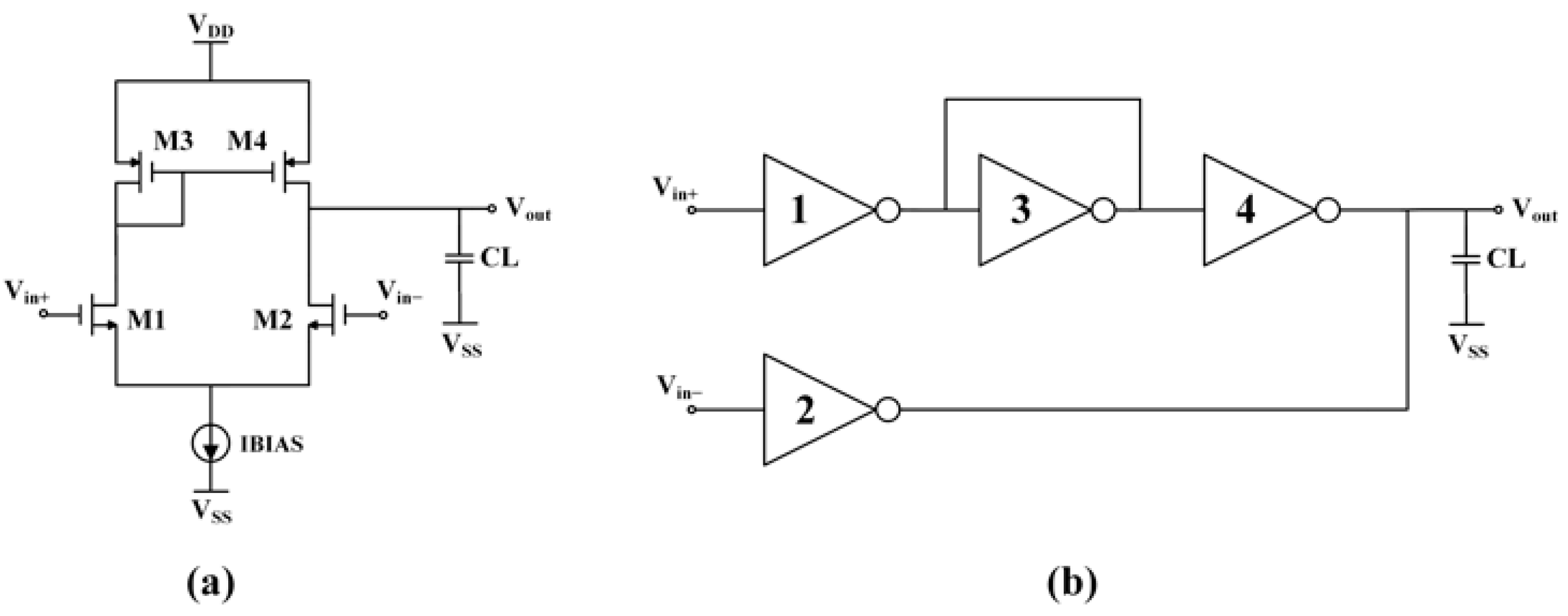
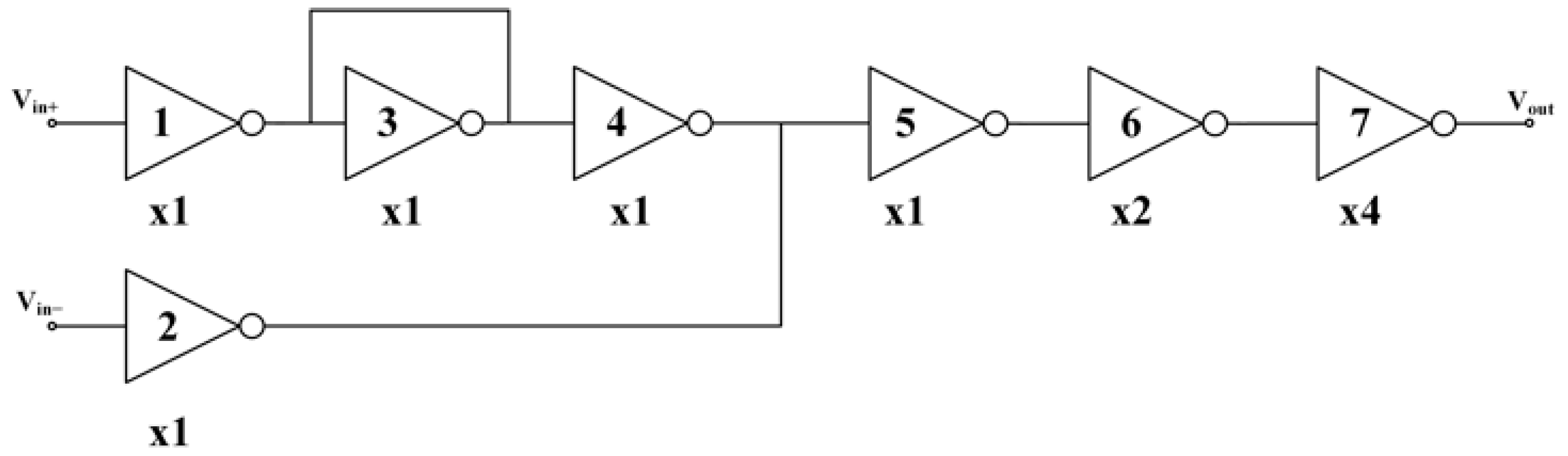
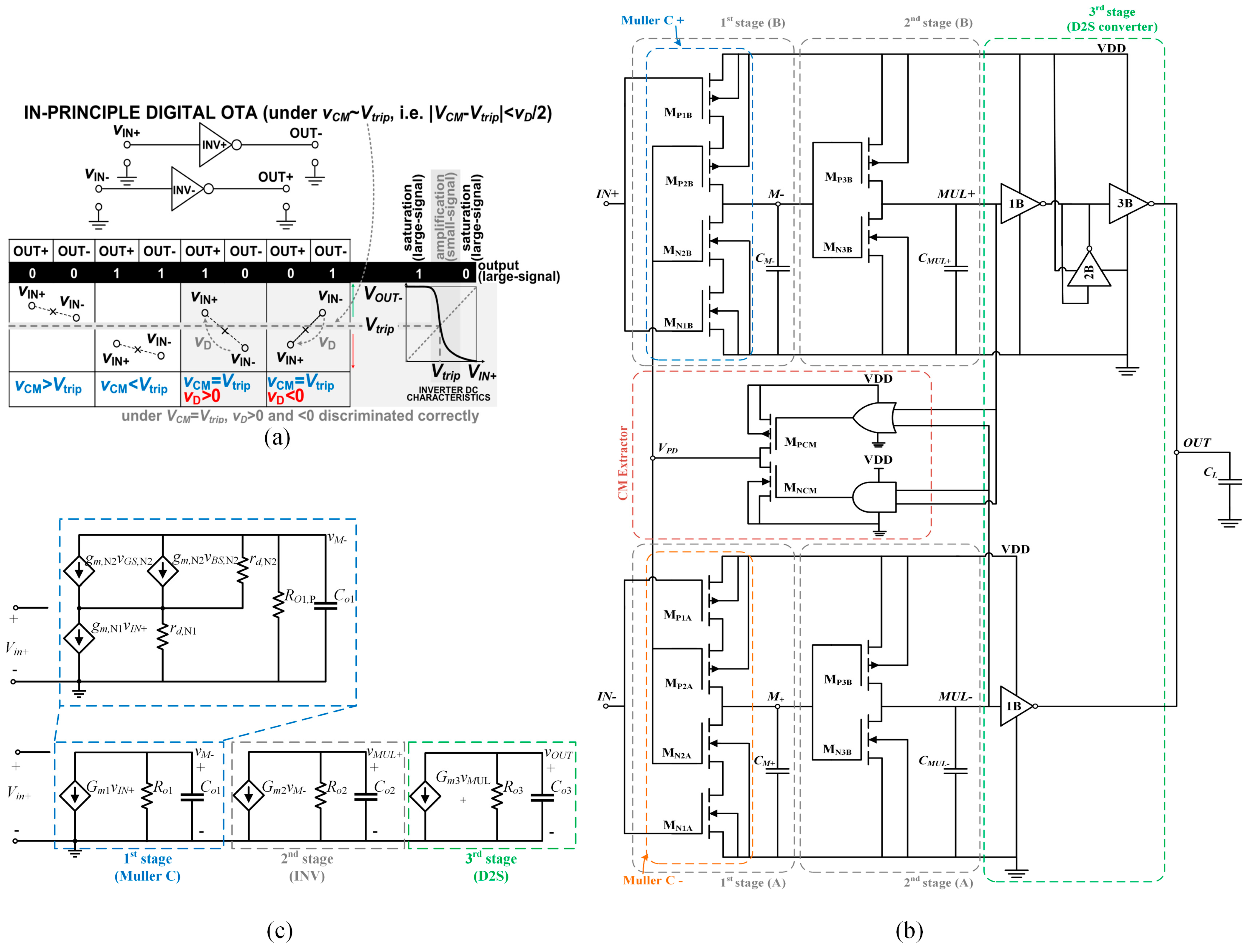
All the previous OTAs require manual design flow from the schematic level to the layout and routing. Moreover, the BD and BB approaches especially result in considerable area occupation because separate wells must be used. In other words, unlike digital designs, the previous OTAs do not take advantage of design automation and technology scaling.
The inverter-based (INV) approach exploits CMOS inverters as transconductance stage elements, as said, in an attempt to extend the digital design flow to the analog domain, keep low the design effort, and provide portability across technologies. An early implementation of this approach is the so-called Nauta transconductor and further derivations [34,35,36,37,38,39,40,41,42].
As an introduction, consider the inverter M1–M2 in Figure 5 and neglect, for the moment, resistor RF. It can be seen that the inverter works as an amplifier, provided that it is biased in its switching threshold so that both transistors are in saturation. Under this biasing condition, the small-signal transconductance of the inverter is equal to the sum of the transconductances of both the nMOS and pMOS transistors, i.e., gm = gm1 + gm2.
The bias point can be obtained through self-biasing using the resistive feedback provided by RF, as shown in Figure 5, or with more complex, higher-efficiency topologies [40], even exploiting the body terminal [37]. In conclusion, the circuit in Figure 5 can be used as a transimpedance amplifier because it has a relatively low input resistance.
To obtain a transconductance amplifier, we can return to a conventional single-stage OTA, as exemplified in Figure 6a. The key concept here is to replace each transistor in the signal path (M1–M4) with an inverter. The gate and the drain of the original transistors correspond to the input and output of the associated inverter, respectively. The source terminal is not important, as it is kept at a fixed potential. This is true for active load transistors M3 and M4 but also for the pair M1 and M2, since, as is well known, the common source is at the virtual ground, provided that the input signal is purely differential. As a result, the circuit in Figure 6b is derived, which represents the basic inverter-based single-stage OTA. Indicating with Gmi and Roi the transconductance and output resistance of the i-th inverter, the output voltage is given by Vout = (Gm1Gm4/Gm3 Vin+Gm2 Vin)Ro4. If Gm1 = Gm2 = Gm1,2, and Gm3 = Gm4, then the gain can be expressed as
A = G m 1 , 2 R o 4
The expression of GBW is as in (6) by replacing gm1,2 with Gm1,2 and C1 with CL. (In this case, dominant pole compensation is adopted.)
While this circuit can be designed using standard cells and automated place and route, it has several drawbacks, such as low DC gain and CMRR (due to the unavoidable mismatches between Gm1 and Gm2 and between Gm3 and Gm4), it implements only a pseudo-differential OTA, and it does not offer DC current control [42]. The latter limitation is fundamental for applications with a limited power budget. Moreover, it makes the solution very sensitive to process, supply, and temperature (PVT) variations.
A four-stage inverter-based OTA that uses the bulk terminals of both the p-channel and n-channel MOS transistors of the standard-cell inverter as current and voltage control inputs was proposed in [43]. The body-control approach is similar to that used in digital applications to handle process variations. All the standard-cell inverters used for analog functions are connected to an analog building block generator, which provides the bulk voltages and which, in turn, enables each cell’s static output voltage to be adjusted to half the supply voltage and the quiescent current to be set to a multiple of a reference current. The simplified schematic of the OTA proposed in [43] is shown in Figure 7, where inverters 1–5 are simple inverters (×1), inverter 6 is made up of two parallel inverters (×2), and inverter 7 is made up of four parallel inverters (×4). The body-control section is not shown for simplicity, but the interested reader can refer to [43] for further details.
In summary, this solution operates at a 0.5 V supply and provides a DC gain of around 70 dB, a gain–bandwidth product around of 7 MHz, and a slew rate of 1.51 V/µs, with a power consumption of only 0.88 µW.

6. Digital Approach

Analog processing requires a well-defined biasing point for the active devices, which, in turn, require a well-defined quiescent current, setting the lower limit for the DC power consumption. With the digital-based approach, it is possible to eliminate any quiescent bias current and to ensure low power consumption, low area occupation, and low complexity at the cost of weak control over current consumption and hence performance across PVT variations.
Several fully digital OTAs (DIGOTA) with a sub-1 V supply and nanowatt power consumption have been presented in literature [43,44,45,46,47,48,49,50,51]. These solutions do not require a DC current, as they are essentially digital standard cell-based OTAs and share with the inverter-based approach the advantages of both simple design and portability over technologies.
In this context, a passive-less fully-digital operational transconductance amplifier (DIGOTA) that employs time-domain processing, zero bias current, and passive-less self-oscillation common-mode compensation was proposed in [45,46] and finally improved in [51].
The principle of operation of the DIGOTA is the same as the NOT approach and relies on the observation that a simple pair of digital inverters, as shown in Figure 8a, under an input differential signal (VIN+VIN) > 0 ((VIN+VIN) < 0) generates a high (low) output differential voltage, provided that the input common-mode voltage, VCM, is close to the inverter trip point, Vtrip. If VCM is away from Vtrip, the digital outputs of the inverters are equal and cannot discriminate whether (VIN+VIN) > 0, or (VIN+VIN) < 0. However, the information related to the signal VCM < Vtrip or VCM > Vtrip still provides useful information that can be exploited to correct the common-mode input signal and enforce the desired condition, VCM = Vtrip, through a negative feedback loop.
The schematic of the DIGOTA recently introduced in [51] is shown in Figure 8b. The compensation of the common-mode voltage is implemented by adopting an input stage based on the Muller C-element driven by the two input voltages, VIN+ and VIN, and by the signal VPD. The differential-to-single-ended (D2S) output stage is implemented in this work by inverters 1B and 2B (constituting an inverting voltage buffer), with inverters 1A and 3B acting as transconductance amplifiers. As a result, the DIGOTA is made up of three gain stages, namely the Muller C-element, the inverter, and the output stage. Remarkably, it has been demonstrated in [51] that the equivalent small-signal model can be reduced to that of a conventional three-stage OTA, as shown in Figure 8c. Assuming that VPD is almost constant, the small-signal parameters in Figure 8c can be expressed as (Note that a more accurate evaluation of gm,N1 and gm,P1 includes the body transconductance of the transistors MN2 and MP2, as detailed in [51]):
G m 1 = g m , N 1 + g m , P 1
G m 2 = g m , N 3 + g m , P 3
G m 3 = 2 g m N , 1 A + g m P , 3 B
C O 1 = C p a r 1 + C M
C O 2 = C p a r 2 + C M U L
C O 3 = C p a r 3 + C L
R O 1 = R O 1 , N R O 1 , P
R O 2 = r d , N 3 r d , P 3
R O 3 = r d , N 3 r d , P 3
with Cpari being the parasitic capacitance at the output of the i-th stage. RO1,N and RO1,P are the resistances of the cascode gain stage. The voltage gain and the GBW are, therefore, equal to
A = G m 1 G m 2 G m 3 R O 1 R O 2 R O 3
G B W = G m 1 G m 2 G m 3 R O 1 R O 2 C L
Under a 0.3 V supply and a load of 250 pF (and at 27 °C), the power consumption of the OTA is 44.2 nW, while the occupied area is 625 μm2. DC gain is 66 dB, and GBW is 12.3 kHz. Power dissipation ad GBW increases to 198.6nW and 59 kHz at 70 °C, just to give and idea of the sensitivity of temperature.

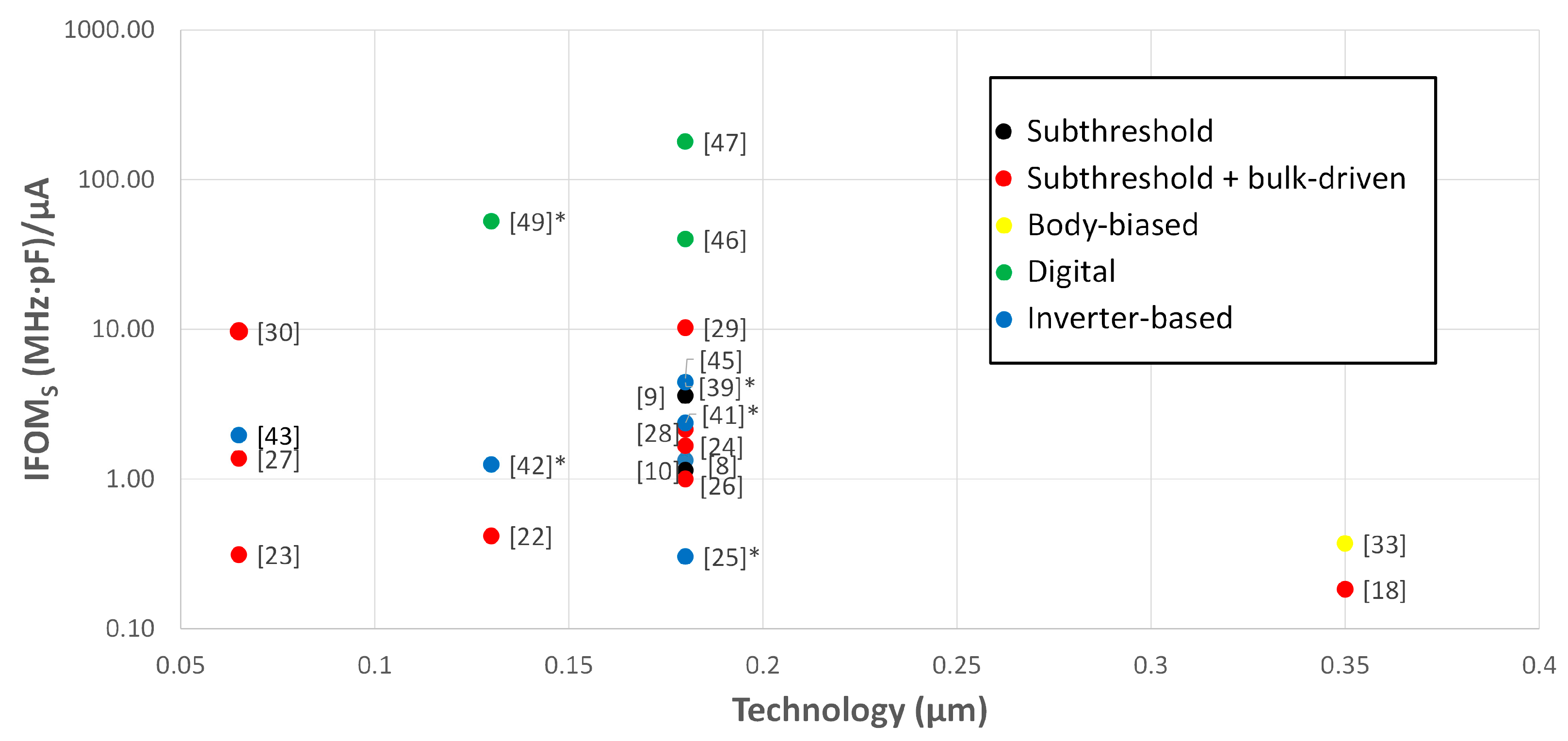
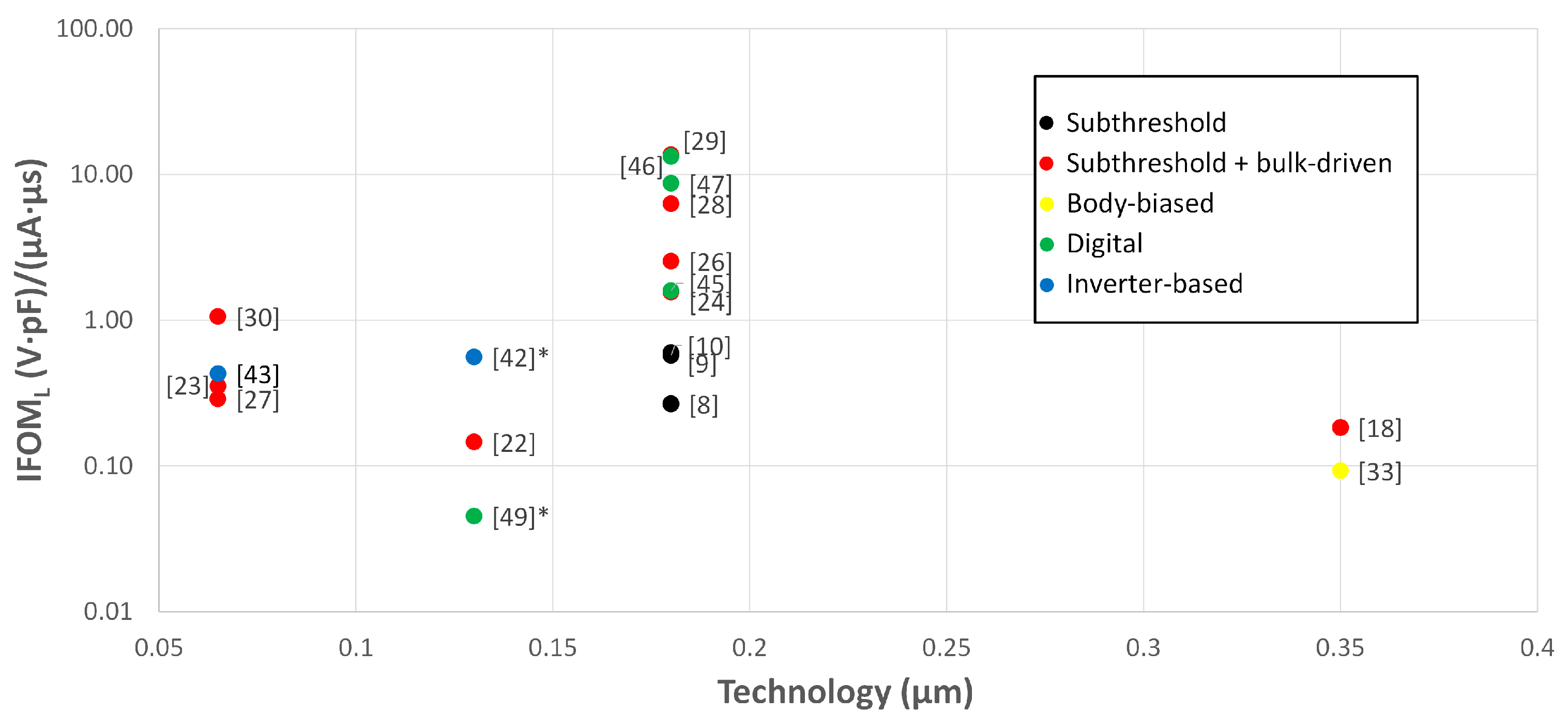
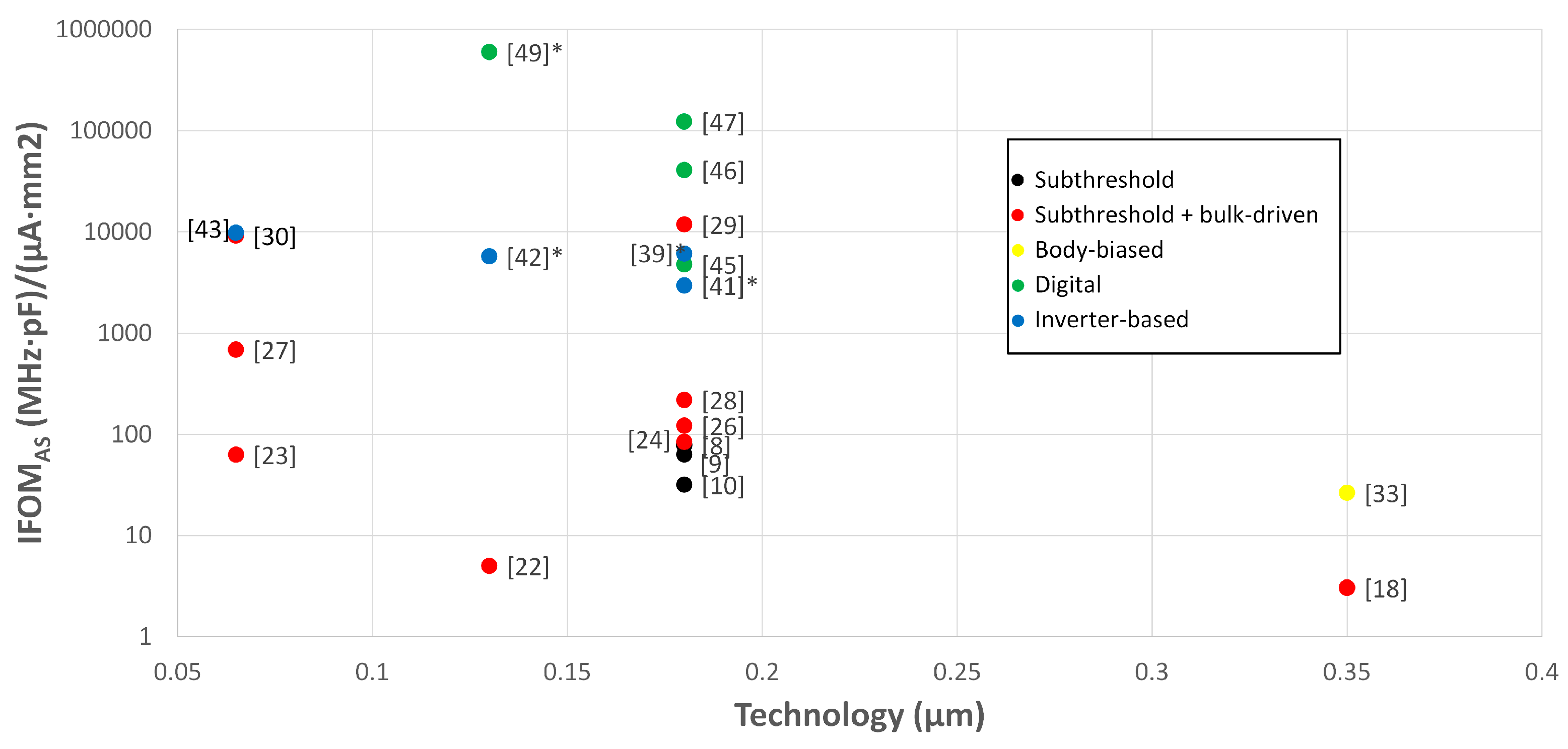
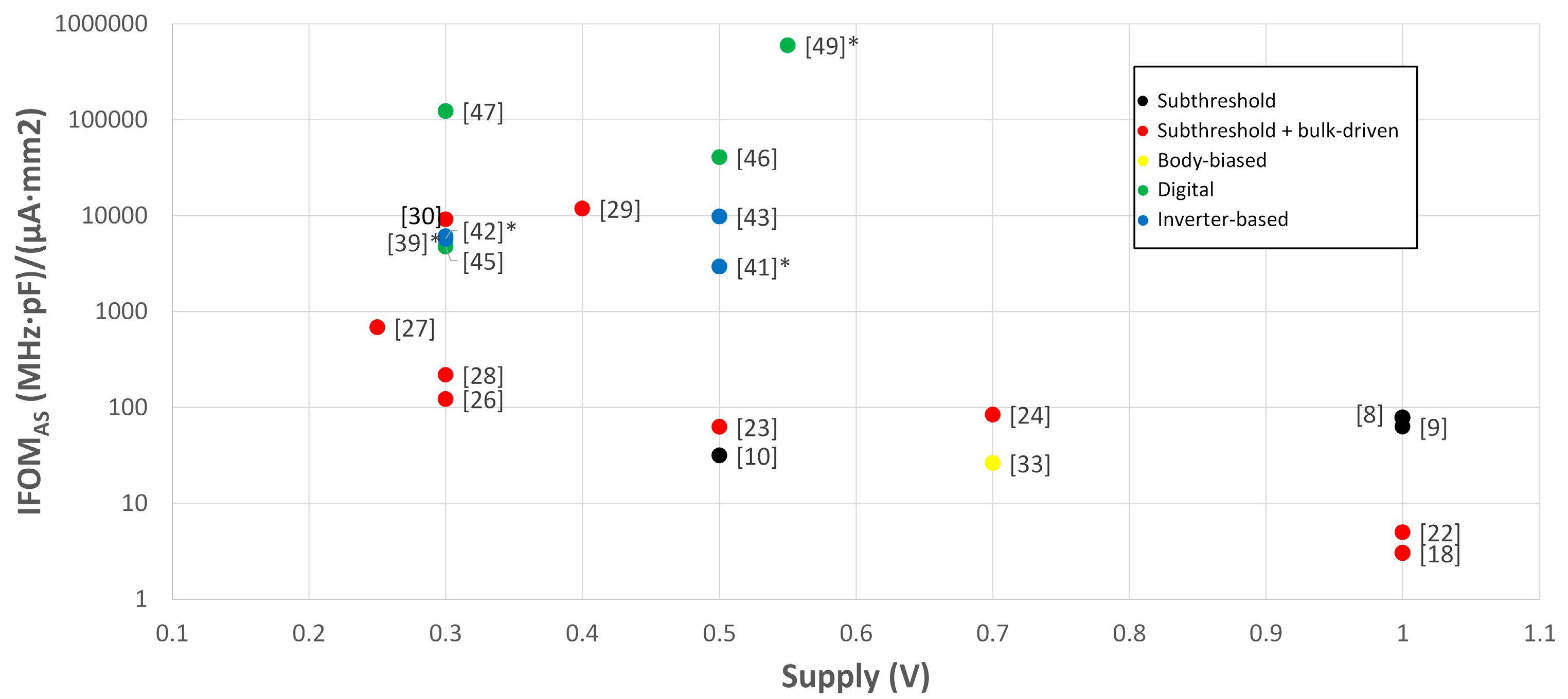
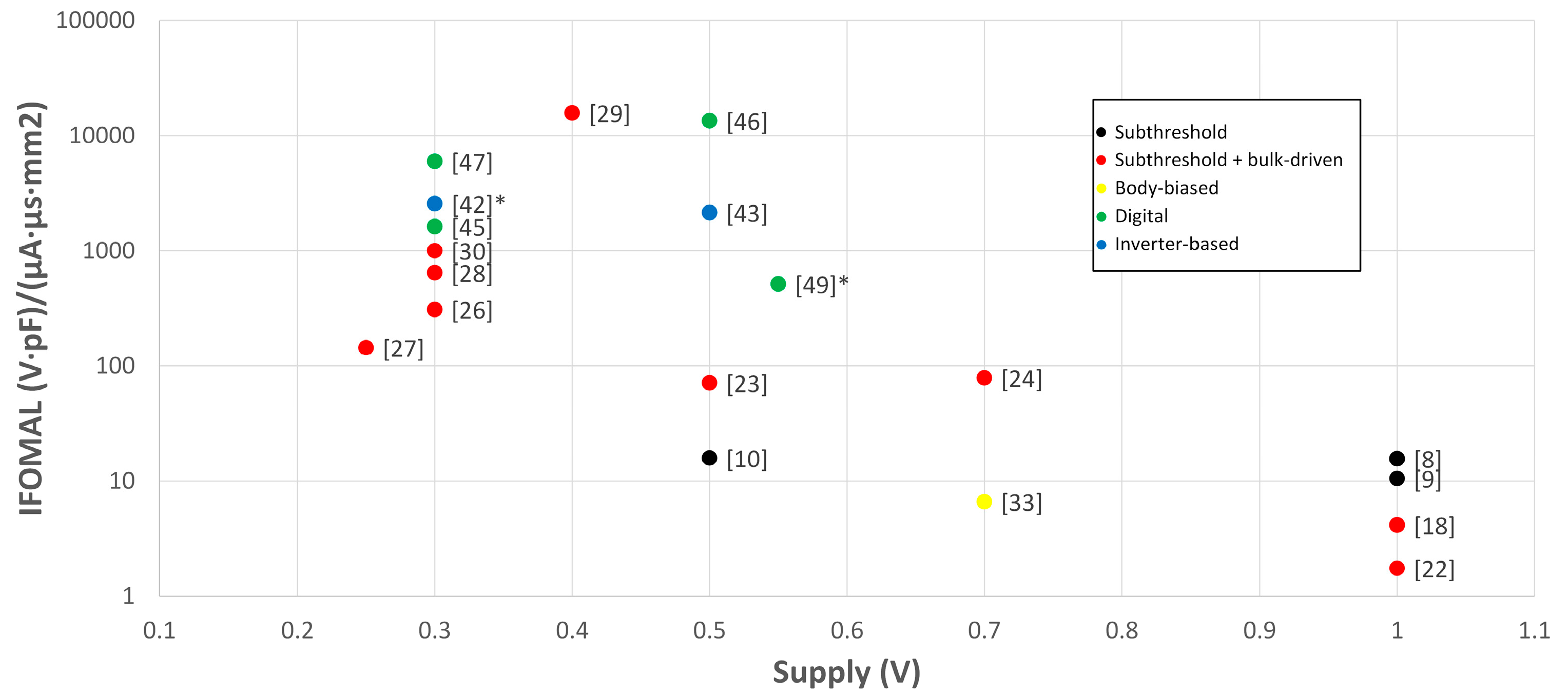
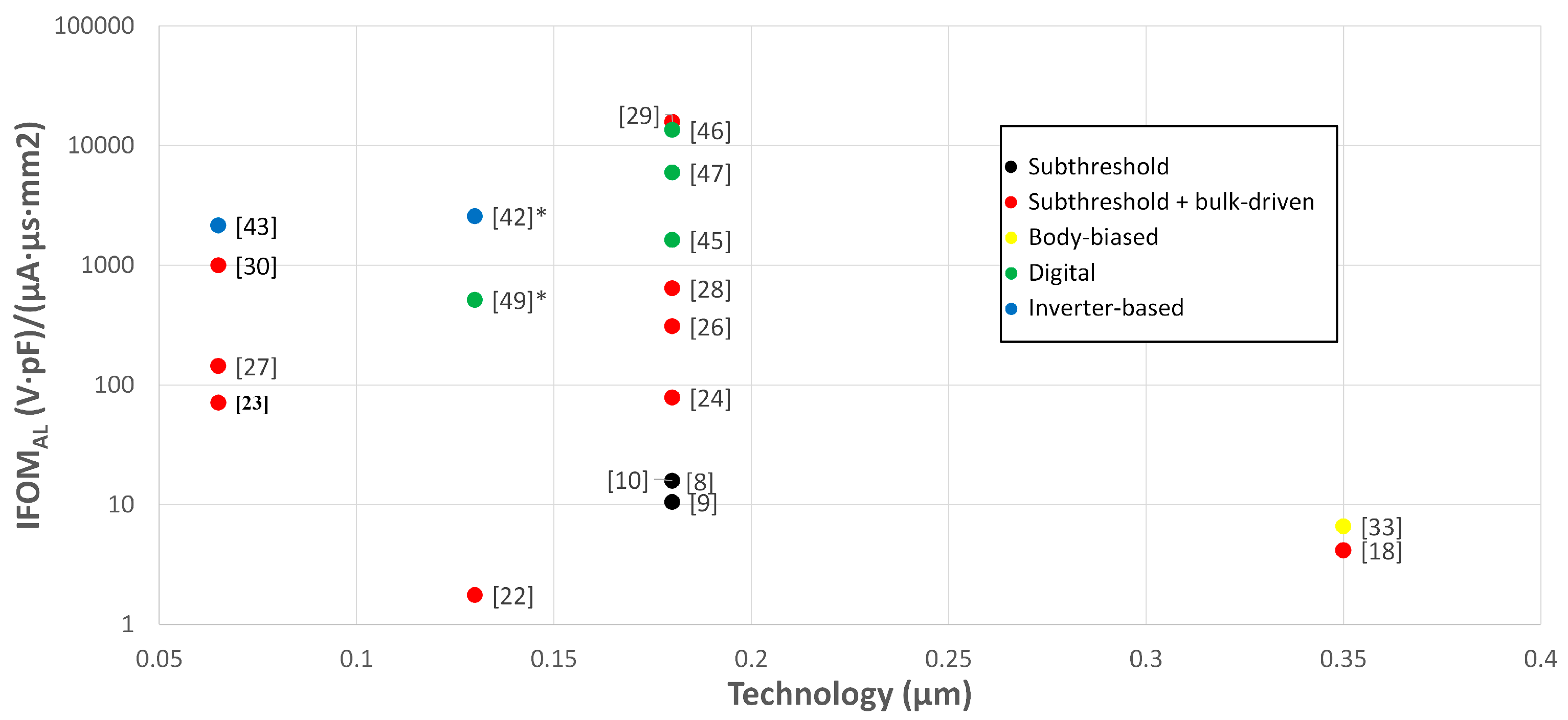
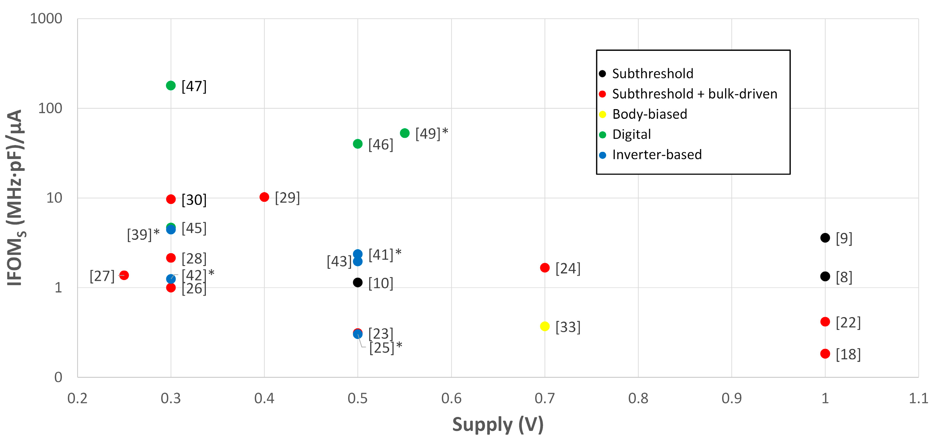
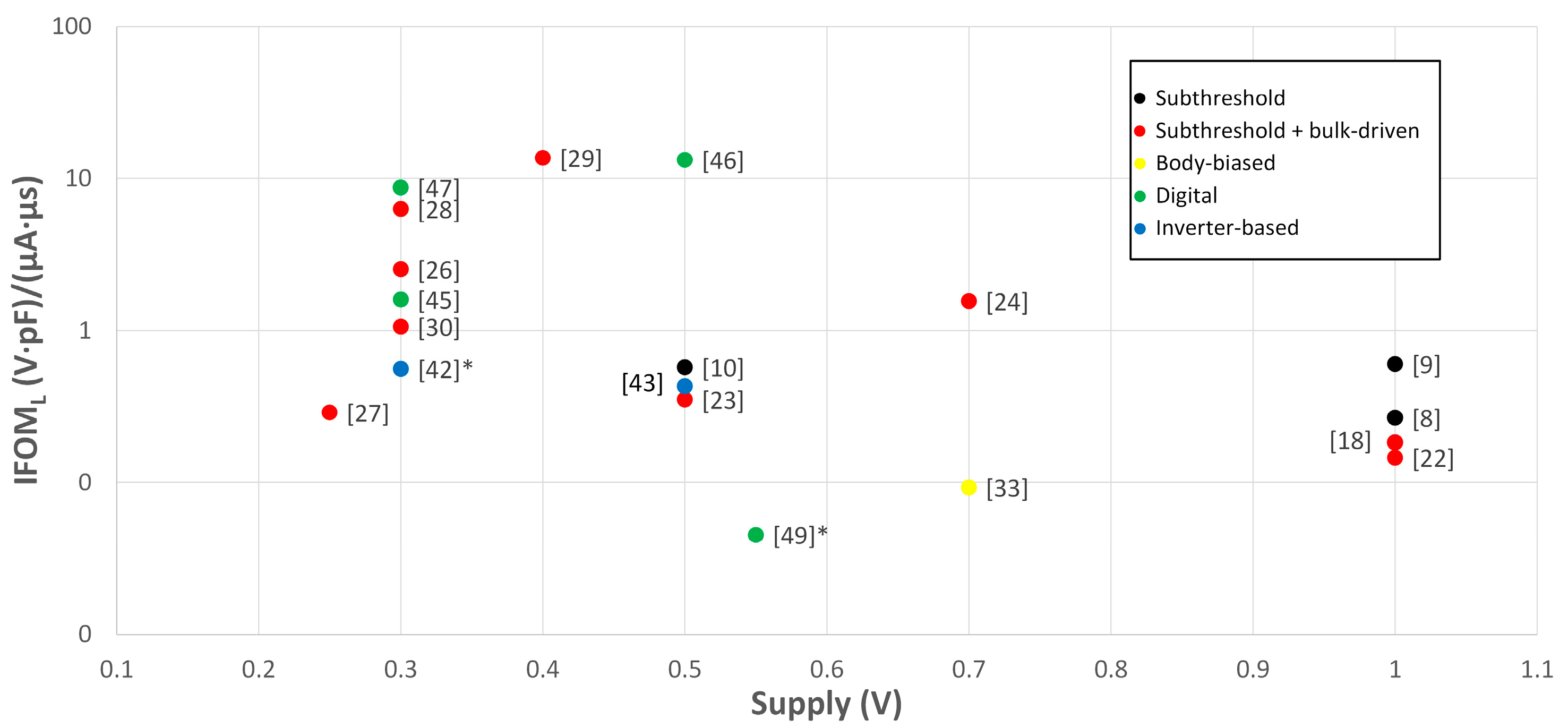
7. Comparison and Discussion

With a view of making a more detailed comparison among the examined approaches, we will consider only the ultra-low power OTAs with a supply equal to or less than 0.7 V, which are summarized in Table 2. Note that simulated INV solutions have also been considered, due to the lack of fabricated examples. The main OTA parameters such as DC gain, gain–bandwidth product (GBW), phase margin (PM), slew rate (SR), noise, common-mode rejection ratio (CMRR), and power supply rejection ratio (PSRR), together with the well-known figures of merit, FOMS, FOML, IFOMS, and IFOML [10,11,21,22,23,26,27,51], defined in (18) and (19), are evaluated.
F O M S = G B W P o w e r C L
F O M L = S R P o w e r C L
I F O M S = G B W I T C L
I F O M L = S R I T C L
where IT is the total bias current.
For a specified capacitance load, (22)–(25) show a trade-off between small-signal and large-signal parameters and total power/bias current consumption.
If we also consider the area occupation, we can define the following two additional figures of merit (IFOMAS and IFOMAL) in (24) and (25) [30,46,51]
I F O M A S = G B W A r e a · I T C L
I F O M A L = S R A r e a · I T C L
From the inspection of Table 2, the lowest value of power consumption, which was around 1 nW, was achieved by [39,47], which used a DIG and an INV approach, respectively. The highest value of the DC gain was 98 dB and was achieved by [28], which combined the BD and the SUB approach, while the highest GBW was achieved by [23] (with minimum CL of 3pF), which exploited an INV approach.
The highest IFOMS was achieved by the INV OTA proposed in [47], while the highest IFOML was achieved by the BD + SUB OTA proposed in [29]. It is also apparent that the DIG and INV approach resulted in the lowest area occupation.
Figure 9 and Figure 10 show the plots of IFOMS and IFOML (on a semilogarithmic scale) for the different OTAs as functions of the technology node. Additionally, IFOMS and IFOML reached the maximum in the 0.18 mm technology node, and the best small-signal performance was achieved by the DIG approach, whereas DIG and SUB + BD shared the best large-signal performance. Interestingly, SUB + BD was still the best in the minimum technology node implementations (i.e., 65-nm), though no DIG implementations here are available for comparison.
Figure 11 and Figure 12 also show IFOMAS and IFOMAL as functions of the technology node. In general, the highest values of IFOMAS were achieved by the DIG and INV approaches, thanks to their inherent reduced area occupation. SUB + BD was competitive for the large-signal performance.
Another comparison was carried out considering the effect of the supply voltage reduction, as illustrated in Figure 13 and Figure 14, showing the IFOMS and IFOML as functions of VDD, respectively. Below 0.6 V, DIG approaches provided the best IFOMS, which were greater up to one order of magnitude with respect to INV and SUB-BD counterparts. IFOML were dominated by SUB-BD and DIG approaches, which provided similar values.
Considering also the area occupation, Figure 15 and Figure 16 show the IFOMAS and IFOMAL achieved by the OTAs as functions of the supply voltage. Similar considerations for Figure 13 and Figure 14 can be derived.

8. Conclusions

This paper describes OTA solutions amenable for IoT applications that require low-voltage and low-current capabilities together with reduced area occupation. After providing a succinct examination of the working principles of the CMOS subthreshold, body-driving, body-biasing, inverter-based, and digital techniques by the utilization of exemplifying solutions proposed by the authors, a comparison of cutting-edge CMOS OTA designs suitable for IoT applications was performed. The comparison was carried out by taking into account small-signal and large-signal performances, as well as area occupation and robustness against PVT variations. According to the findings, only the SUB + BD, DIG, and INV approaches are suitable for supply voltages less than 0.6 V. Furthermore, DIG and INV require the least amount of silicon area, provide design portability across multiple technologies, and support automated design. SUB + BD, on the other hand, which is an ‘analog’ approach, necessitates a custom design and a larger area but maintains performance across technology scaling, providing competitive large-signal performance. It was noted that the SUB + BD approach continues to provide the best results in the smallest technology node implementations available, namely 65 nm (although this may be due to a lack of DIG implementations in this technology). More importantly, with a well-defined bias point, it allows for better control over power dissipation (and thus small- and large-signal performances) in the face of PVT variations.
In summary, applications requiring reliable current control must prefer SUB + BD or at the very least, INV, with current control solutions if silicon area is a major concern. DIG solutions, while promising, will require further study and development.

Author Contributions

Conceptualization: A.D.G. and S.P.; data curation: C.V.; original draft preparation: A.D.G. and S.P.; writing—review and editing: all authors; formal analysis: all authors; supervision: A.D.G. and S.P. All authors have read and agreed to the published version of the manuscript.

Funding

This work was funded by the European Union (NextGeneration EU) through the MUR PNRR project SAMOTHRACE (ECS00000022).

Conflicts of Interest

The authors declare no conflict of interest.

Abbreviations

BBBulk-Biased
BDBulk-Driven
CADComputer-Aided Design
CMOSComplementary Metal–Oxide–Semiconductor
CMRRCommon-Mode Rejection Ratio
DIGOTADigital OTA
GBWGain–Bandwidth product
IoTInternet of Things
MOSMetal–Oxide–Semiconductor
OTAOperational Transconductance Amplifier
PMPhase Margin
PSRRPower Supply Rejection Ratio
PVTProcess, Supply, and Temperature
SRSlew Rate

References

  1. Number of Internet of Things (IoT) Connected Devices Worldwide from 2019 to 2021, with Forecasts from 2022 to 2030. Available online: https://www.statista.com/statistics/1183457/iot-connected-devices-worldwide/ (accessed on 6 September 2023).
  2. Alioto, M. (Ed.) Enabling the Internet of Things: From Integrated Circuits to Integrated Systems; Springer International Publishing: Berlin/Heidelberg, Germany, 2017; ISBN 978-3-319-51480-2. [Google Scholar]
  3. Jang, T.; Kim, G.; Kempke, B.; Henry, M.B.; Chiotellis, N.; Pfeiffer, C.; Kim, D.; Kim, Y.; Foo, Z.; Kim, H.; et al. Circuit and System Designs of Ultra-Low Power Sensor Nodes with Illustration in a Miniaturized GNSS Logger for Position Tracking: Part I—Analog Circuit Techniques. IEEE Trans. Circuits Syst. Regul. Pap. 2017, 64, 2237–2249. [Google Scholar] [CrossRef]
  4. Sansen, W. 1.3 Analog CMOS from 5 Micrometer to 5 Nanometer. In Proceedings of the 2015 IEEE International Solid-State Circuits Conference—(ISSCC) Digest of Technical Papers, San Francisco, CA, USA, 22–26 February 2015; pp. 1–6. [Google Scholar]
  5. Vittoz, E.; Fellrath, J. CMOS Analog Integrated Circuits Based on Weak Inversion Operations. IEEE J. Solid-State Circuits 1977, 12, 224–231. [Google Scholar] [CrossRef]
  6. Hollis, T.M.; Comer, D.J.; Comer, D.T. Optimization of MOS Amplifier Performance through Channel Length and Inversion Level Selection. IEEE Trans. Circuits Syst. II Express Briefs 2005, 52, 545–549. [Google Scholar] [CrossRef]
  7. Valero Bernal, M.R.; Celma, S.; Medrano, N.; Calvo, B. An Ultralow-Power Low-Voltage Class-AB Fully Differential OpAmp for Long-Life Autonomous Portable Equipment. IEEE Trans. Circuits Syst. II Express Briefs 2012, 59, 643–647. [Google Scholar] [CrossRef]
  8. Chatterjee, S.; Tsividis, Y.; Kinget, P. 0.5-V Analog Circuit Techniques and Their Application in OTA and Filter Design. IEEE J. Solid-State Circuits 2005, 40, 2373–2387. [Google Scholar] [CrossRef]
  9. Magnelli, L.; Amoroso, F.A.; Crupi, F.; Cappuccino, G.; Iannaccone, G. Design of a 75-nW, 0.5-V Subthreshold Complementary Metal–Oxide–Semiconductor Operational Amplifier. Int. J. Circuit Theory Appl. 2014, 42, 967–977. [Google Scholar] [CrossRef]
  10. Qin, Z.; Tanaka, A.; Takaya, N.; Yoshizawa, H. 0.5-V 70-nW Rail-to-Rail Operational Amplifier Using a Cross-Coupled Output Stage. IEEE Trans. Circuits Syst. II Express Briefs 2016, 63, 1009–1013. [Google Scholar] [CrossRef]
  11. Grasso, A.D.; Marano, D.; Palumbo, G.; Pennisi, S. Design Methodology of Subthreshold Three-Stage CMOS OTAs Suitable for Ultra-Low-Power Low-Area and High Driving Capability. IEEE Trans. Circuits Syst. Regul. Pap. 2015, 62, 1453–1462. [Google Scholar] [CrossRef]
  12. Blalock, B.J.; Allen, P.E.; Rincon-Mora, G. Designing 1-V Op Amps Using Standard Digital CMOS Technology. IEEE Trans. Circuits Syst. II Analog Digit. Signal Process. 1998, 45, 769–780. [Google Scholar] [CrossRef]
  13. Bialko, M.; Guzinski, A.; Allen, P.E.; Blalock, B.J.; Rincon-Mora, G. Comments on “Designing 1-V Op-Amps Using Standard Digital CMOS Technology” [and Reply]. IEEE Trans. Circuits Syst. II Analog Digit. Signal Process. 1999, 46, 1448. [Google Scholar] [CrossRef]
  14. Lehmann, T.; Cassia, M. 1-V Power Supply CMOS Cascode Amplifier. IEEE J. Solid-State Circuits 2001, 36, 1082–1086. [Google Scholar] [CrossRef]
  15. Stockstad, T.; Yoshizawa, H. A 0.9-V 0.5-Um Rail-to-Rail CMOS Operational Amplifier. IEEE J. Solid-State Circuits 2002, 37, 286–292. [Google Scholar] [CrossRef]
  16. Carrillo, J.M.; Duque-Carrillo, J.F.; Torelli, G.; Ausin, J.L. Constant-g/Sub m/Constant-Slew-Rate High-Bandwidth Low-Voltage Rail-to-Rail CMOS Input Stage for VLSI Cell Libraries. IEEE J. Solid-State Circuits 2003, 38, 1364–1372. [Google Scholar] [CrossRef]
  17. Carrillo, J.M.; Torelli, G.; Perez-Aloe Valverde, R.; Duque-Carrillo, J.F. 1-V Rail-to-Rail CMOS OpAmp With Improved Bulk-Driven Input Stage. IEEE J. Solid-State Circuits 2007, 42, 508–517. [Google Scholar] [CrossRef]
  18. Ferreira, L.H.C.; Pimenta, T.C.; Moreno, R.L. An Ultra-Low-Voltage Ultra-Low-Power CMOS Miller OTA with Rail-to-Rail Input/Output Swing. IEEE Trans. Circuits Syst. II Express Briefs 2007, 54, 843–847. [Google Scholar] [CrossRef]
  19. Monsurrò, P.; Pennisi, S.; Scotti, G.; Trifiletti, A. 0.9-V CMOS Cascode Amplifier with Body-Driven Gain Boosting. Int. J. Circuit Theory Appl. 2009, 37, 193–202. [Google Scholar] [CrossRef]
  20. Raikos, G.; Vlassis, S. Low-Voltage Bulk-Driven Input Stage with Improved Transconductance. Int. J. Circuit Theory Appl. 2011, 39, 327–339. [Google Scholar] [CrossRef]
  21. Zuo, L.; Islam, S.K. Low-Voltage Bulk-Driven Operational Amplifier with Improved Transconductance. IEEE Trans. Circuits Syst. Regul. Pap. 2013, 60, 2084–2091. [Google Scholar] [CrossRef]
  22. Ferreira, L.H.C.; Sonkusale, S.R. A 60-dB Gain OTA Operating at 0.25-V Power Supply in 130-Nm Digital CMOS Process. IEEE Trans. Circuits Syst. Regul. Pap. 2014, 61, 1609–1617. [Google Scholar] [CrossRef]
  23. Abdelfattah, O.; Roberts, G.W.; Shih, I.; Shih, Y.C. An Ultra-Low-Voltage CMOS Process-Insensitive Self-Biased OTA With Rail-to-Rail Input Range. IEEE Trans. Circuits Syst. Regul. Pap. 2015, 62, 2380–2390. [Google Scholar] [CrossRef]
  24. Cabrera-Bernal, E.; Pennisi, S.; Grasso, A.D.; Torralba, A.; Carvajal, R.G. 0.7-V Three-Stage Class-AB CMOS Operational Transconductance Amplifier. IEEE Trans. Circuits Syst. Regul. Pap. 2016, 63, 1807–1815. [Google Scholar] [CrossRef]
  25. Vlassis, S.; Kulej, T.; Khateb, F.; Souliotis, G. 0.5 V Bulk-Driven Ring Amplifier Based on Master–Slave Technique. Analog Integr. Circuits Signal Process. 2017, 90, 189–197. [Google Scholar] [CrossRef]
  26. Kulej, T.; Khateb, F. Design and Implementation of Sub 0.5-V OTAs in 0.18-Μm CMOS. Int. J. Circuit Theory Appl. 2018, 46, 1129–1143. [Google Scholar] [CrossRef]
  27. Woo, K.-C.; Yang, B.-D. A 0.25-V Rail-to-Rail Three-Stage OTA With an Enhanced DC Gain. IEEE Trans. Circuits Syst. II Express Briefs 2020, 67, 1179–1183. [Google Scholar] [CrossRef]
  28. Kulej, T.; Khateb, F. A 0.3-V 98-dB Rail-to-Rail OTA in 0.18 μm CMOS. IEEE Access 2020, 8, 27459–27467. [Google Scholar] [CrossRef]
  29. Ballo, A.; Grasso, A.D.; Pennisi, S. 0.4-V, 81.3-nA Bulk-Driven Single-Stage CMOS OTA with Enhanced Transconductance. Electronics 2022, 11, 2704. [Google Scholar] [CrossRef]
  30. Ballo, A.; Grasso, A.D.; Pennisi, S.; Susinni, G. A 0.3-V 8.5-μ A Bulk-Driven OTA. IEEE Trans. Very Large Scale Integr. VLSI Syst. 2023, 31, 1444–1448. [Google Scholar] [CrossRef]
  31. Grasso, A.D.; Monsurrò, P.; Pennisi, S.; Scotti, G.; Trifiletti, A. Analysis and Implementation of a Minimum-Supply Body-Biased CMOS Differential Amplifier Cell. IEEE Trans. Very Large Scale Integr. VLSI Syst. 2009, 17, 172–180. [Google Scholar] [CrossRef]
  32. Centurelli, F.; Monsurro, P.; Pennisi, S.; Scotti, G.; Trifiletti, A. Design Solutions for Sample-and-Hold Circuits in CMOS Nanometer Technologies. IEEE Trans. Circuits Syst. II Express Briefs 2009, 56, 459–463. [Google Scholar] [CrossRef]
  33. Grasso, A.D.; Pennisi, S.; Scotti, G.; Trifiletti, A. 0.9-V Class-AB Miller OTA in 0.35-μm CMOS With Threshold-Lowered Non-Tailed Differential Pair. IEEE Trans. Circuits Syst. Regul. Pap. 2017, 64, 1740–1747. [Google Scholar] [CrossRef]
  34. Nauta, B. A CMOS Transconductance-C Filter Technique for Very High Frequencies. IEEE J. Solid-State Circuits 1992, 27, 142–153. [Google Scholar] [CrossRef]
  35. Andreani, P.; Mattisson, S. On the Use of Nauta’s Transconductor in Low-Frequency CMOS g/Sub m/-C Bandpass Filters. IEEE J. Solid-State Circuits 2002, 37, 114–124. [Google Scholar] [CrossRef]
  36. Figueiredo, M.; Santos-Tavares, R.; Santin, E.; Ferreira, J.; Evans, G.; Goes, J. A Two-Stage Fully Differential Inverter-Based Self-Biased CMOS Amplifier with High Efficiency. IEEE Trans. Circuits Syst. Regul. Pap. 2011, 58, 1591–1603. [Google Scholar] [CrossRef]
  37. Shrimali, H.; Chatterjee, S. 11 GHz UGBW Op-Amp with Feed-Forward Compensation Technique. In Proceedings of the 2011 IEEE International Symposium of Circuits and Systems (ISCAS), Rio de Janeiro, Brazil, 15–18 May 2011; pp. 17–20. [Google Scholar]
  38. Kaliyath, Y.; Laxminidhi, T. A 1.8 V 11.02 μW Single-Ended Inverter-Based OTA with 113.62 dB Gain. In Proceedings of the 2016 IEEE Distributed Computing, VLSI, Electrical Circuits and Robotics (DISCOVER), Mangalore, India, 13–14 August 2016; pp. 237–241. [Google Scholar]
  39. Rodovalho, L.H.; Aiello, O.; Rodrigues, C.R. Ultra-Low-Voltage Inverter-Based Operational Transconductance Amplifiers with Voltage Gain Enhancement by Improved Composite Transistors. Electronics 2020, 9, 1410. [Google Scholar] [CrossRef]
  40. Bae, W. CMOS Inverter as Analog Circuit: An Overview. J. Low Power Electron. Appl. 2019, 9, 26. [Google Scholar] [CrossRef]
  41. Manfredini, G.; Catania, A.; Benvenuti, L.; Cicalini, M.; Piotto, M.; Bruschi, P. Ultra-Low-Voltage Inverter-Based Amplifier with Novel Common-Mode Stabilization Loop. Electronics 2020, 9, 1019. [Google Scholar] [CrossRef]
  42. Sala, R.D.; Centurelli, F.; Scotti, G. A Novel Differential to Single-Ended Converter for Ultra-Low-Voltage Inverter-Based OTAs. IEEE Access 2022, 10, 98179–98190. [Google Scholar] [CrossRef]
  43. Centurelli, F.; Giustolisi, G.; Pennisi, S.; Scotti, G. A Biasing Approach to Design Ultra-Low-Power Standard-Cell-Based Analog Building Blocks for Nanometer SoCs. IEEE Access 2022, 10, 25892–25900. [Google Scholar] [CrossRef]
  44. Crovetti, P.S. A Digital-Based Analog Differential Circuit. IEEE Trans. Circuits Syst. Regul. Pap. 2013, 60, 3107–3116. [Google Scholar] [CrossRef]
  45. Toledo, P.; Crovetti, P.; Aiello, O.; Alioto, M. Fully Digital Rail-to-Rail OTA With Sub-1000-Μm2 Area, 250-mV Minimum Supply, and nW Power at 150-pF Load in 180 Nm. IEEE Solid-State Circuits Lett. 2020, 3, 474–477. [Google Scholar] [CrossRef]
  46. Toledo, P.; Crovetti, P.; Aiello, O.; Alioto, M. Design of Digital OTAs With Operation Down to 0.3 V and nW Power for Direct Harvesting. IEEE Trans. Circuits Syst. Regul. Pap. 2021, 68, 3693–3706. [Google Scholar] [CrossRef]
  47. Toledo, P.; Crovetti, P.; Klimach, H.; Bampi, S.; Aiello, O.; Alioto, M. A 300mV-Supply, Sub-nW-Power Digital-Based Operational Transconductance Amplifier. IEEE Trans. Circuits Syst. II Express Briefs 2021, 68, 3073–3077. [Google Scholar] [CrossRef]
  48. Toledo, P.; Rubino, R.; Musolino, F.; Crovetti, P. Re-Thinking Analog Integrated Circuits in Digital Terms: A New Design Concept for the IoT Era. IEEE Trans. Circuits Syst. II Express Briefs 2021, 68, 816–822. [Google Scholar] [CrossRef]
  49. Palumbo, G.; Scotti, G. A Novel Standard-Cell-Based Implementation of the Digital OTA Suitable for Automatic Place and Route. J. Low Power Electron. Appl. 2021, 11, 42. [Google Scholar] [CrossRef]
  50. Toledo, P.; Crovetti, P.S.; Klimach, H.D.; Musolino, F.; Bampi, S. Low-Voltage, Low-Area, nW-Power CMOS Digital-Based Biosignal Amplifier. IEEE Access 2022, 10, 44106–44115. [Google Scholar] [CrossRef]
  51. Privitera, M.; Crovetti, P.S.; Grasso, A.D. A Novel Digital OTA Topology with 66-dB DC Gain and 12.3-kHz Bandwidth. IEEE Trans. Circuits Syst. II Express Briefs 2023. early access. [Google Scholar] [CrossRef]
  52. Ramirez-Angulo, J.; Carvajal, R.G.; Tombs, J.; Torralba, A. Low-Voltage CMOS Op-Amp with Rail-to-Rail Input and Output Signal Swing for Continuous-Time Signal Processing Using Multiple-Input Floating-Gate Transistors. IEEE Trans. Circuits Syst. II Analog Digit. Signal Process. 2001, 48, 111–116. [Google Scholar] [CrossRef]
  53. Ramirez-Angulo, J.; Lopez-Martin, A.J.; Carvajal, R.G.; Chavero, F.M. Very Low-Voltage Analog Signal Processing Based on Quasi-Floating Gate Transistors. IEEE J. Solid-State Circuits 2004, 39, 434–442. [Google Scholar] [CrossRef]
  54. Rajput, K.K.; Saini, A.K.; Bose, S.C. DC Offset Modeling and Noise Minimization for Differential Amplifier in Subthreshold Operation. In Proceedings of the 2010 IEEE Computer Society Annual Symposium on VLSI, Lixouri, Greece, 5–7 July 2010; pp. 247–252. [Google Scholar]
  55. Di Cataldo, G.; Grasso, A.D.; Pennisi, S.; Scotti, G.; Trifiletti, A. CMOS Non-Tailed Differential Pair: CMOS Non-Tailed Differential Pair. Int. J. Circuit Theory Appl. 2015, 44, 1468–1477. [Google Scholar] [CrossRef]
  56. Khateb, F. Bulk-Driven Floating-Gate and Bulk-Driven Quasi-Floating-Gate Techniques for Low-Voltage Low-Power Analog Circuits Design. AEU-Int. J. Electron. Commun. 2014, 68, 64–72. [Google Scholar] [CrossRef]
Figure 1. Schematic of the three-stage CMOS OTA operating in the subthreshold region proposed in [11]. © 2015 IEEE. Reprinted, with permission, from Design Methodology of Subthreshold Three-Stage CMOS OTAs Suitable for Ultra-Low-Power Low-Area and High Driving Capability.
Electronics 12 04361 g001
Figure 2. (a) Gate-driven and (b) bulk-driven p-channel differential pairs.
Electronics 12 04361 g002
Figure 3. Schematic of the OTA with positive feedback proposed in [29].
Electronics 12 04361 g003
Figure 4. (a) Minimum-supply differential pair (b) common-mode control circuit proposed in [31].
Electronics 12 04361 g004
Figure 5. The CMOS inverter uses an analog amplifier that is self-biased at the switching threshold.
Electronics 12 04361 g005
Figure 6. Conventional (a) and inverter-based (b) single-stage OTA.
Electronics 12 04361 g006
Figure 7. Schematic of the inverter-based OTA in [43].
Electronics 12 04361 g007
Figure 8. (a) Principle of operation of the DIGOTA introduced in [46]; (b) schematic and (c) small-signal model of the DIGOTA proposed in [51]. © 2023 IEEE. Reprinted, with permission, from A novel Digital OTA topology with 66-dB DC Gain and 12.3-kHz Bandwidth.
Electronics 12 04361 g008
Figure 9. IFOMS vs. technology (* simulated).
Electronics 12 04361 g009
Figure 10. IFOML vs. technology (* simulated).
Electronics 12 04361 g010
Figure 11. IFOMAS vs. technology (* simulated).
Electronics 12 04361 g011
Figure 12. IFOMAL vs. technology (* simulated).
Electronics 12 04361 g012
Figure 13. IFOMS vs. supply voltage (* simulated).
Electronics 12 04361 g013
Figure 14. IFOML vs. supply voltage (* simulated).
Electronics 12 04361 g014
Figure 15. IFOMAS vs. supply voltage (* simulated).
Electronics 12 04361 g015
Figure 16. IFOMAL vs. supply voltage (* simulated).
Electronics 12 04361 g016
Table 1. Small-signal parameters of an N-channel MOS transistor (saturation region).
SubthresholdAbove Threshold
Bulk-Driven
g m = I D V G S I D n V T (1a) 2 K W I D L (1b)
g m b = I D V B S λ B g m (2a) C B C C G C g m (2b)
g d s = I D V D S λ I D (3a) λ I D (3b)
f T g m 2 π C G S + C G D + C G B (4a) g m b 2 π C S B + C D B + C b s u b (4b)
gm: gate-source transconductance, gmb: body-source transconductance, gds: drain-source conductance, fT: transition frequency, ID: drain current; W: transistor channel width, L: transistor channel length, VT: thermal voltage, n: subthreshold slope, μn: electron mobility, COX specific gate capacitance, K = μnCOX: transconductance factor, λB: body effect coefficient, λ: channel-length modulation coefficient, CGS: gate-to-source capacitance; CGD: gate-to-drain capacitance; CGB: gate-to-bulk capacitance; CSB: source-to-bulk capacitance; CDB: drain-to-bulk capacitance; CB-sub: bulk-to-substrate capacitance, CBC: bulk-to-channel capacitance; CGC: gate-to-channel capacitance.
Table 2. Comparison of ultra-low-power OTAs (* simulated).
[8][9][10][18][22][23][24][26][28][27][29][30][33][25] *[41] *[39] *[43][42] *[45][47][46][49]
Year2005201420162007201420152016201820202020202220232017201720202020202220222020202120212021
Tech. [μm]0.180.180.180.350.130.0650.180.180.180.0650.180.0650.350.180.180.180.0650.130.180.180.180.13
Op. modebSUBSUBSUBSUB, BDSUB, BDSUB, BDBDSUB, BDSUB, BDSUB, BDSUB, BDBDBBINVINVINVINVINVDIGDIGDIGDIG
Area [mm2] × 10−21.75.73.668.30.520.810.20.90.111.4-0.080.070.020.020.10.10.10.01
Supply [V]0.50.50.50.60.250.50.70.30.30.250.40.30.70.50.50.30.50.30.30.30.50.55
CL [pF]203040151532020301515050102010100.5215080150250
DC gain [dB]627077696046576398.1703738659125.2516434.9730307387
IT [μA]1500.150.140.90.072366360.0560.0430.1040.0818.527260.5580.0021.7520.30.0080.0020.21514.9
Power [μW]750.0750.070.540.01818325.20.0170.0130.0260.0332.5518.9130.2790.0010.8756.10.0020.0010.1088.2
GBW [kHz]0.0118411238,000300033106165010003941320.74685012,7000.24603150
PM [°]605556655357606154887970.3605987906262-54-65
SR [V/ms)200032150.743,00028007927.9180250---151056800.10.2192.7
Noise [nV/sqrt(Hz)]280310-29033009261001850 *1800 *--2506531.8-809--21,000--175
CMRR (dB)65-5574.5-3519726062.53639.845--37-2741-6546
PSRR [dB]43-52--37526261383044.750122.376.841--30-5039
# stages2222233233132---4-----
FOMS [MHz·pF/μW]2.677.202.290.311.670.622.383.337.155.4825.632.350.530.614.7314.83.914.1615.659880.296.0
FOML [(V/μs)·pF/μW]0.531.201.140.420.580.72.228.45211.1534.13.530.13---0.861.865.3128.9626.50.08
IFOMS
[MHz·pF/μA]
1.333.601.140.180.420.311.6712.151.3710.39.710.370.302.374.441.961.254.6917940.152.8
IFOML
[(V/μs)·pF/μA]
0.270.600.570.250.150.351.562.546.30.2913.641.060.09---0.430.561.598.6913.30.05
IFOMAS
[MHz·pF/μA·mm2]
78.4363.1631.7535638412221968511,838915626.5-29576107978657304773122,62740,852598,189
IFOMAL [[(V/μs)·pF/μA·mm2]15.6910.5315.874.21.871.278.6309.2642.9144.215,7459996.6---215025651623594313,499513
Disclaimer/Publisher’s Note: The statements, opinions and data contained in all publications are solely those of the individual author(s) and contributor(s) and not of MDPI and/or the editor(s). MDPI and/or the editor(s) disclaim responsibility for any injury to people or property resulting from any ideas, methods, instructions or products referred to in the content.

