Article

Refined Analysis of Leakage Current in SiC Power Metal Oxide Semiconductor Field Effect Transistors after Heavy Ion Irradiation

1
Xinjiang Technical Institute of Physics and Chemistry, Chinese Academy of Sciences, Urumqi 830011, China
2
Xinjiang Key Laboratory of Electronic Information Material and Device, Urumqi 830011, China
3
University of Chinese Academy of Sciences, Beijing 100049, China
*
Authors to whom correspondence should be addressed.
Electronics 2023, 12(20), 4349; https://doi.org/10.3390/electronics12204349
Submission received: 24 August 2023 / Revised: 5 October 2023 / Accepted: 17 October 2023 / Published: 20 October 2023
(This article belongs to the Special Issue Radiation Effects of Advanced Electronic Devices and Circuits)

Abstract

:
A leakage current is the most critical parameter to characterize heavy ion radiation damage in SiC MOSFETs. An accurate and refined analysis of the source and generation process of a leakage current is the key to revealing the failure mechanism. Therefore, this article finely tests the online and post-irradiation leakage changes and leakage pathways of SiC MOSFETs caused by heavy ion irradiation, analyzes the damaged location of the device in reverse, and discusses the mechanism of leakage generation. The experimental results further confirm that an increase in the leakage current of a device during heavy ion irradiation is positively correlated with the applied voltage of the drain, but the leakage path is not direct from the drain to the source. The experimental analysis of the source of the leakage current of the device after irradiation indicates that there is also a leakage current path between the device gate and source. The research results suggest that the experimental sample is more prone to a single-event gate rupture effect under this heavy ion radiation condition. The gate breakdown mainly occurs in the gate oxide layer at the neck region. This research can provide a theoretical basis for the radiation resistance reinforcement of SiC power devices.

1. Introduction

With the rapid development of China’s aerospace technology, the demand for high-performance, high-power devices is becoming increasingly urgent [1,2]. SiC MOSFETs have shown broad application prospects in the aerospace field due to their superior performance in high temperature resistance, low loss, fast switching speed, and high blocking voltage [3,4]. However, high-energy particles present in space can cause radiation damage to electronic devices, thereby affecting device performance and reliability [5,6,7]. For SiC power devices, although SiC materials have a comprehensive bandgap structure and strong radiation resistance, they still exhibit significant single-event radiation effects due to the process structure and operating characteristics of the device, leading to severe leakage and even burnout [6,8,9,10], seriously hindering their rapid application in the aerospace field. At present, the damage mechanisms of single-event burnout (SEB) and single-event gate rupture (SEGR) induced by heavy ions in space are difficulties and hot topics in the study of single-event effects in SiC MOSFETs [11,12,13].
A leakage current is the most critical parameter for characterizing heavy ion radiation damage in SiC MOSFETs [14,15,16]. Existing research has shown that before the occurrence of SEB or SEGR in SiC MOSFETs, phenomena such as gate leakage current IG and drain leakage current ID increases occur [15,17,18]. Among them, the mechanism of an SEB effect is the occurrence of an abnormal bulk current, which leads to a sharp increase in the lattice temperature of the device, resulting in a local thermal burnout of the device [19,20,21,22,23]; the mechanism of the SEGR effect is that a transient additional electric field is generated in the gate dielectric layer that exceeds the critical electric field, causing the gate oxide layer to be broken down [14,24,25,26,27]. But, the specific occurrence of SEB or SEGR is closely related to the location of the formation of an internal leakage current in the device. Therefore, in-depth research and refined analysis of the source and location of SiC power MOSFET leakage caused by heavy ion radiation are crucial to revealing the mechanisms of SEB and SEGR effects.
The increase in the leakage current of SiC MOSFETs caused by single-event effects is mainly due to the radiation-induced gate current IG and the drain current ID. IG especially comes from a breakdown current and an ionization current [16,19]; a breakdown current is a leakage current caused by the breakdown of the gate oxide layer caused by the electric field generated by the incident particles between the gate and drain [16,28]; an ionization current is the current generated by the excitation or ionization of atoms or electrons in the gate oxide layer by incident particles. The ID mainly comes from the transport of holes and electrons in the channel and the increase in the drain leakage current caused by ionization and reverse breakdown effects in the drain structure caused by incident particles [28,29,30,31]. Although the values of IG and ID are related to the energy, angle, and position of the incident particles [14,32] and the process and structure of the device, the main influencing factor is the device’s leakage source operating voltage VDS. In general, the larger the VDS, the greater the radiation-induced leakage of the device. Generally, when the VDS is greater than 50% of the rated voltage, it will cause the device to experience SEB or SEGR effects [33].
In summary, although a large number of studies have identified an increase in the device leakage current during heavy ion radiation and even the occurrence of SEB and SEGR effects, these are mainly due to the decrease in gate oxide insulation performance (breakdown) and drain structure damage caused by heavy ion radiation. But, the master–slave or quantitative relationship between these two damage mechanisms and radiation environment, device technology, and structural changes is still unclear, and more experimental verification is needed. In addition, the location of gate oxide breakdown and leakage structure damage varies, and the leakage paths of the device will not be the same. As shown in Figure 1, the leakage paths for gate oxide leakage IG include gate leakage IGD and IGS (Figure 1, ① and ②), while the leakage paths for drain leakage ID include IGD and IDS (Figure 1, ③ and ④), red-dashed ellipses on the schematic diagram show the possible locations of damage. There is also a lack of detailed research and analysis of these leakage paths. The analysis of these leakage pathways and the determination of damage locations are the theoretical basis for strengthening SiC power MOSFETs against single-event radiation damage.
Therefore, this experiment conducted single-event irradiation tests on SiC MOSFETs with different leakage source voltages and monitored the leakage current of the device during irradiation online. The I-V characteristics of the device before and after irradiation were compared, and the leakage current at each electrode of the device was finely tested. The path of a leakage current caused by heavy ions was analyzed and determined to determine the damage location of the device in reverse. The research results further deepen the understanding of the mechanism of a single-event radiation damage effect in SiC MOSFETs, providing a theoretical basis for the radiation hardening of SiC power devices.

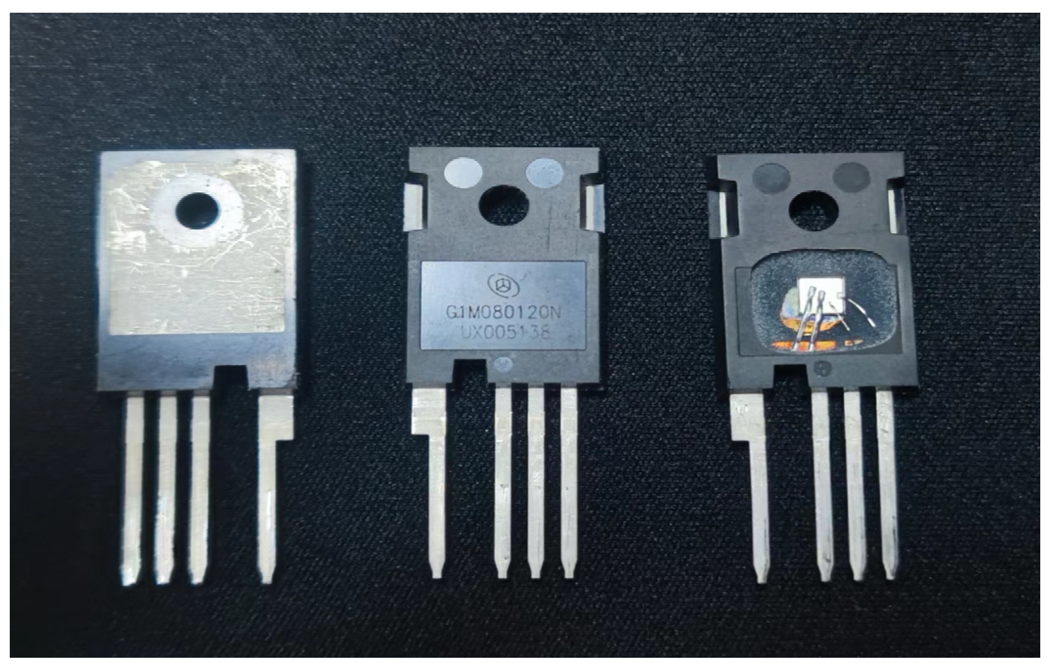
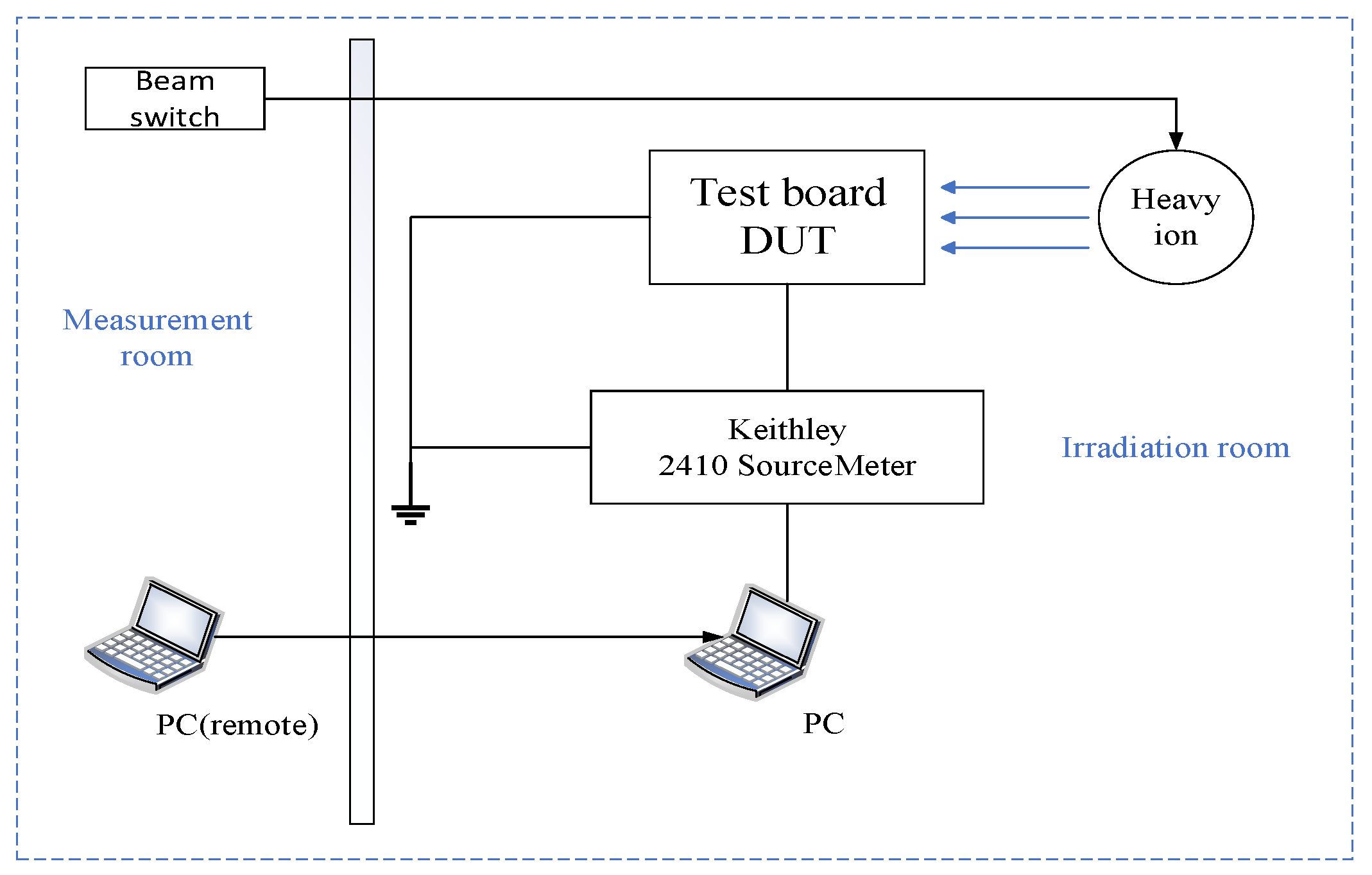
2. Materials and Methods
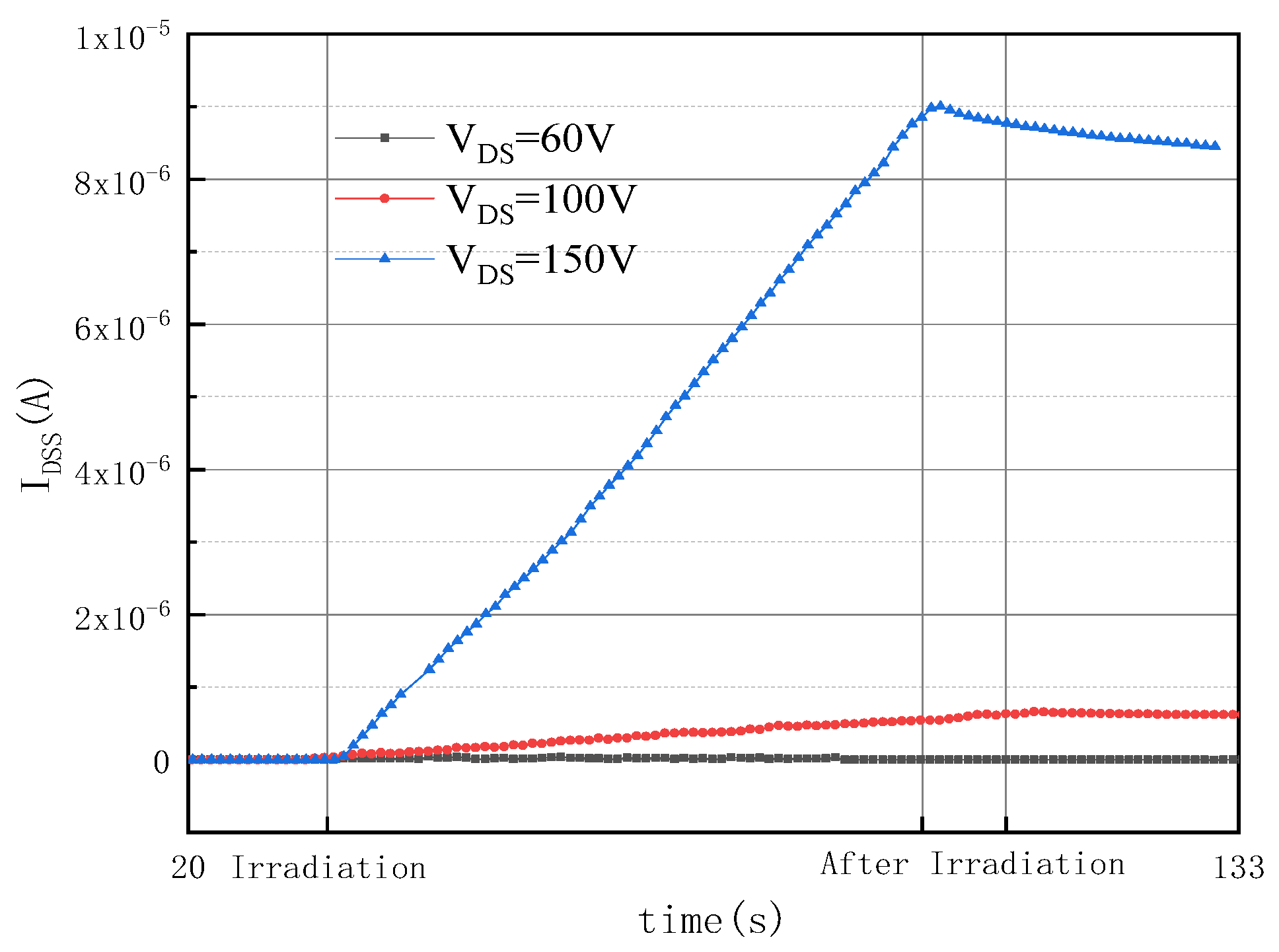
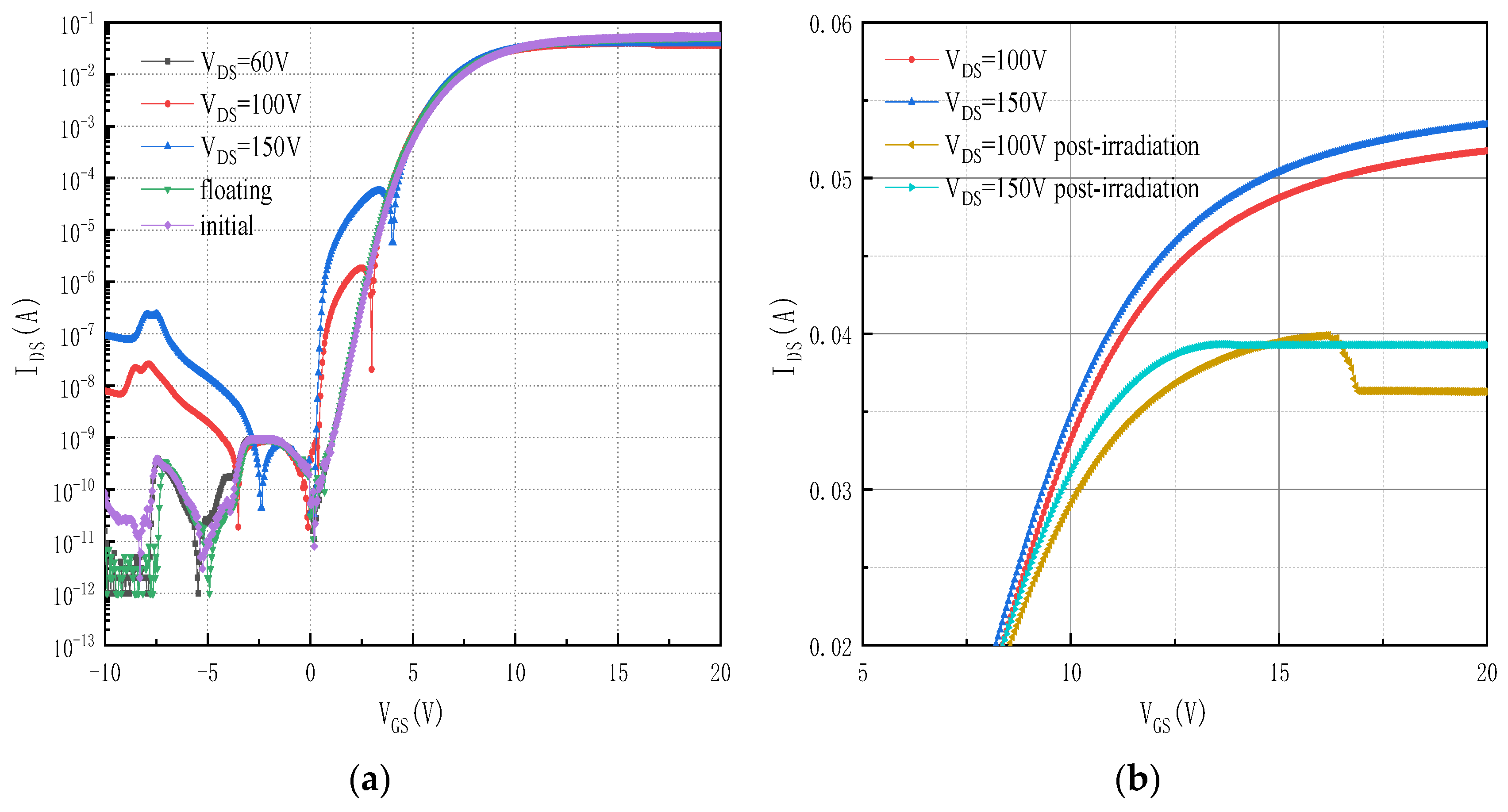
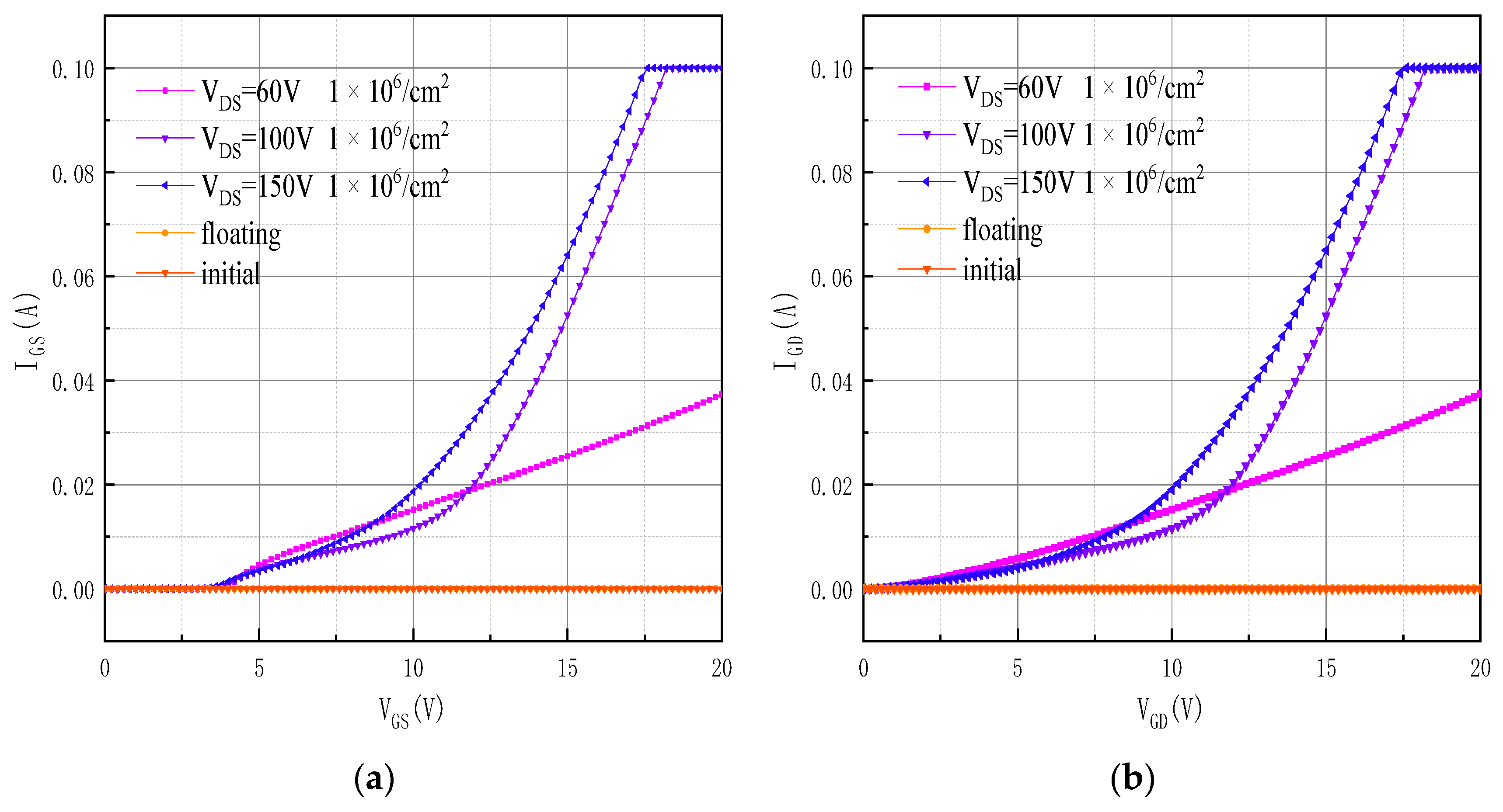
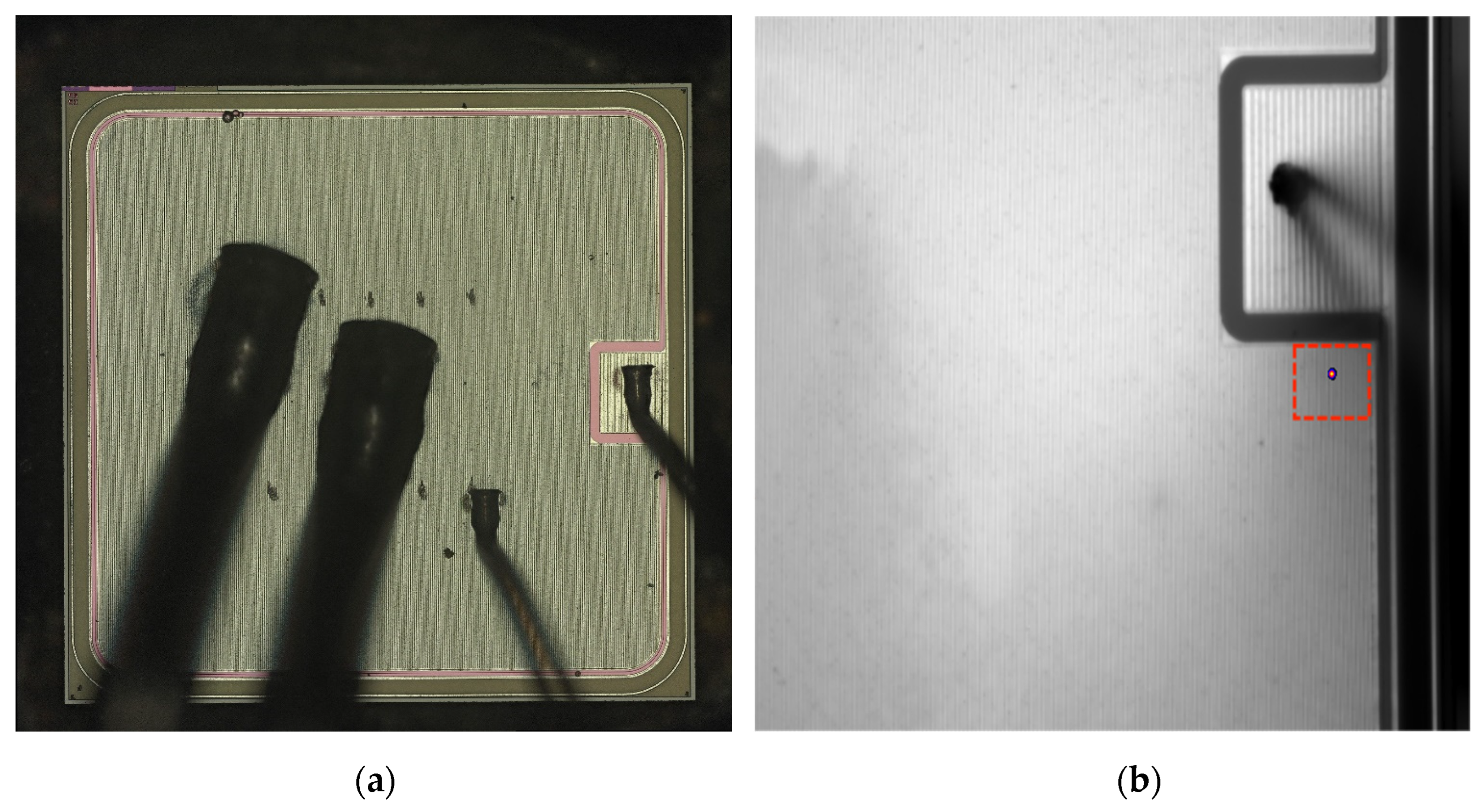
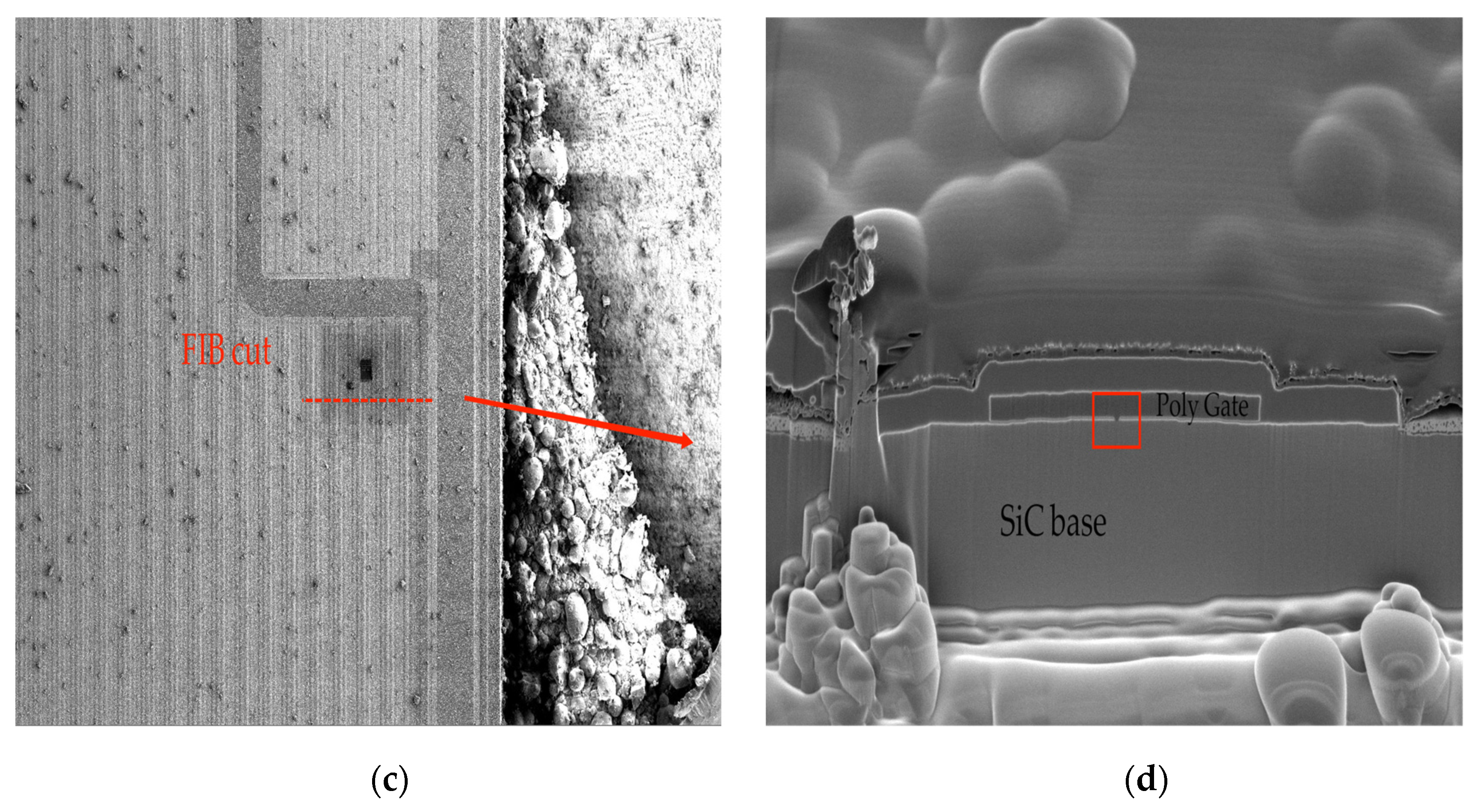
The device used in the irradiation experiment is a typical planar gate structure, N-channel SiC power MOSFET packaged in TO-247L. The device parameters are VDS = 1200 V, ID = 40 A, and RDS(on) = 80 mΩ. A total of 10 test devices were used in the radiation test, including two for each of the three types of drain bias irradiation, floating irradiation and control devices. The device was unpacked before radiation, allowing heavy ions to irradiate the chip surface directly. Device packaging and internal chip morphology of the planar gate SiC MOSFET are shown in Figure 2. Electrical performance tests were conducted on the opened devices, and the results showed that opening did not significantly impact device performance.
The heavy ion test was completed at the Lanzhou Institute of Modern Physics, Chinese Academy of Sciences. The irradiated ion was 181Ta ion, the total energy was 2369.8 MeV, the energy reaching the device surface was 1912.1 MeV, and the range was 111.3 μm. The LET value was 76.3 MeV/(mg/cm2), and the beam spot area irradiated on the device surface in an atmospheric environment was about 4.4 cm2, with the incident direction perpendicular to the device surface. The irradiation fluence rate was approximately 1.6 × 104 cm2 s−1, with a total injection rate of 1 × 10⁶/cm2.
During irradiation, in order to explore the changes in the leakage current of the device caused by heavy ions under different drain voltages, different voltages were applied to the drain electrodes of the device: VDS = 60 V, 100 V, and 150 V, respectively, with zero bias on other electrodes. In addition, floating irradiation conditions, with no voltage applied to all electrodes, were also conducted. Under all irradiation bias conditions, a source meter was introduced between the source and drain of the device to monitor the leakage current IDSS online. The schematic diagram of the SiC MOSFET heavy ion irradiation online testing system is shown in Figure 3.
Before and after irradiation, the device’s operating characteristics were tested using the B1500A semiconductor parameter analysis system, produced by Agilent Technologies, a company headquartered in California, United States. The test conditions were gate voltage VGS = 20 V, source bias, and drain scanning from −10 V to 20 V. Current changes in the device under different operating conditions were observed. Also tested were the drain–source leakage current IDS, gate–source leakage current IGS, and the gate–drain leakage current IGD data of the irradiated device; then, the specific damage location of the single-event effect in the device was analyzed.

3. Results

As shown in Figure 4, the device’s drain–source leakage current IDSS, detected during irradiation under different VDS conditions, varies with irradiation time. The figure shows that when VDS = 60 V, the current curve is almost a straight line, and the drain current jumps within an order of magnitude. When VDS = 100 V and 150 V, the drain current during irradiation shows a linear increase trend with irradiation time, and as the drain bias increases, the slope of the drain current change increases, and the growth trend is significantly faster.
After the irradiation stopped, the IDSS of the device with a VDS of 60 V returned to its initial value. In contrast, the IDSS of the device remained unchanged under bias conditions of 100 V and 150 V, indicating that a single-event effect had occurred. As the drain voltage increased, the generated IDSS also increased, showing a positive correlation. However, when the drain voltage was 150 V, the leakage current of the device did not reach the limit current, indicating that the device did not experience a typical single-event burnout phenomenon. Therefore, it can be considered that the IDSS generated by the device under heavy ion irradiation at this time was caused by accumulated damage at the interface between the drain substrate and the drift region [34]. When Ta ions pass through SiC MOSFETs, they interact with the extranuclear electrons of the target atom and deposit energy. When the energy deposition exceeds a certain threshold, the material around the ion orbit will experience a melting phenomenon because the cooling rate of the material is fast, resulting in the melted material rapidly cooling into amorphous solid structures. These amorphous solids formed along the ion incidence path are localized defect clusters composed of high-concentration composite defects [34,35,36]. The high LET value of Ta ions can induce latent tracks in the active region of SiC MOSFETs [34,36,37]. These leakage channels, composed of defect clusters along the ion path, can cause the leakage current of the online monitoring point of the device to increase during continuous heavy ion radiation. So, it was determined that VDS = 60 V did not cause a single-event effect and is the safe voltage of the device. It is preliminarily speculated that a small-current single-event burnout effect occurred between the drain and source electrodes in devices with biases equal to 100 V and 150 V [36]. Subsequent parameter tests were conducted to determine whether a single-event burnout occurred.
The electrical parameters of the device were tested before and after irradiation, and the transfer characteristics of the device under bias and floating conditions (IDS-VGS) are shown in Figure 5. Figure 5a shows that the device transfer characteristic curves and curves after irradiation under different drain–source bias conditions do not show significant drift. The device characteristic curve with VDS of 60 V during irradiation coincides with the device characteristic curve under floating conditions, and there is no significant difference from the initial value; the transfer characteristics of two devices with VDS of 100 V and 150 V during irradiation showed two significant current increases compared to devices with VDS of 60 V, corresponding to gate voltages of −10 V to −2.5 V and 0 V to 5 V, respectively. IDS increased by two to three orders of magnitude compared to devices with 60 V, and the larger the VDS, the more significant the current increase. Figure 5b compares device transfer characteristic curves under different drain bias voltages in linear coordinates. It can be seen from the figure that the drain current of the device decreased after irradiation. Therefore, it is believed not only that the drain junction was damaged but there should also be current leakage at the gate.
To finely analyze the path of the leakage current generated by heavy ion irradiation on the back of the device, which is the specific damage location, using a semiconductor parameter analysis system to test the electrode currents of each electrode of the device, the testing method is: floating either electrode of the device, applying a scanning voltage between the other two electrodes, and connecting a source meter in series at the tested electrode for current testing. Only one electrode is applied with voltage, and the other two electrodes are connected to ammeters and grounded. The current flowing through this electrode should be the sum of the currents at the other two electrodes. Therefore, it is believed that the existence of current leakage paths between the two electrodes of the device can be judged by the specific current division. Firstly, a scanning voltage was applied on the gate electrode and a test current between the gate–source and the gate–drain. Figure 6 shows the test results of the gate–source current IGS and the gate–drain current IGD of the device obtained using this method. The device irradiation conditions corresponding to each curve in Figure 4 and Figure 5 are (A) VDS = 60 V 1 × 10⁶/cm2, (B) VDS = 100 V 1 × 10⁶/cm2, (C) VDS = 150 V 1 × 10⁶/cm2, (D) device floating 1 × 10⁶/cm2, and (E) device initial value.
The trend of the IGS leakage current at both electrodes of the gate–source in Figure 6a is almost consistent with that of the IGD leakage current at both electrodes of the gate–drain in Figure 6b. After applying a scanning voltage to the gate, all devices with floating electrodes during irradiation did not experience an increase in current, which is consistent with non-irradiated devices; the current of devices with a drain bias voltage applied during irradiation shows an increasing trend. Among them, devices with irradiation biases VDS of 150 V and 100 V reach current limits at a gate voltage of 17 V and 18 V, respectively. Devices with a bias VDS of 60 V neither show any changes like floating devices nor increase the current limit slowly, unlike devices with a high drain bias.
Since the gate oxide layer is an insulating layer, it can be seen from the initial value test of the device before irradiation that the gate current hardly changes with an increase in gate voltage. However, an increased device leakage current after irradiation indicates shallow damage to the gate oxide layer. It is worth noting that the three IGS curves in Figure 6a do not immediately increase after the scanning voltage is applied, indicating that there is no direct current leakage channel between the gate and source electrodes; that is, the damage location is not directly between the gate and source electrodes. All three curves gradually increase after the gate voltage reaches around 2.5 V because as the gate voltage gradually increases, which means VGS is greater than the device threshold voltage; the channel region gradually depletes and approaches strong inversion and extends towards the neck region, forming an n-type layer along the surface coupled to the source electrode. When the gate oxide layer is damaged in the neck area, a leakage channel is formed and reaches the current limit. The IGD curve in Figure 6b immediately increased after voltage was applied, indicating damage between the gate and drain electrodes of the device and a direct leakage channel for the current. Heavy ion irradiation caused damage and destruction of the gate oxide layer, resulting in a single-event gate rupture of the device, with the damage located between the gate and neck regions.
To determine whether a single-event burnout effect occurred between the source and drain of the device, a scanning voltage was applied to the drain electrode, a 0 V bias was applied to both the gate and source electrodes, an ammeter was connected in series on the gate and source electrodes were connected to the ground. The drain current ID, gate current IG, and source current IS were measured. The relationship between them was analyzed, as shown in Figure 7.
Figure 7a shows that the gate current IG and drain leakage current ID of the device, subjected to bias voltage during irradiation, increased directly from 0 V, with almost the same magnitude and in opposite directions. At the same leakage voltage, the current limit is reached, indicating the existence of a current leakage channel between the two electrodes of the gate and drain. The leakage current curve of the floating irradiation device and the non-irradiation device is a straight line, with a value of almost 0. Figure 7b shows that the magnitude of the source current IS is much smaller than that of the drain leakage current ID, fluctuating in the 1 × 10⁻⁹ magnitude. From this, it can be inferred that there is no current leakage channel between the drain and sources. Because there is no damage location between the drain and source electrodes of the device, it can be determined that the test device did not experience single-event burnout.
Based on the above experimental results and analysis, it can be concluded that the leakage current IDSS monitored online in heavy ion irradiation experiments is not caused by the increase in the drain–source current caused by single-event burnout but by the current path caused by a single-event gate rupture, forming a leakage current from the drain electrode to the gate electrode. It should be noted that the leakage current of the device, with an irradiation bias of 60 V, is inconsistent with the online monitoring performance and has reached saturation, which is believed to be caused by the activation of internal defects in the device due to multiple tests and power-ups. Moreover, the voltage at which the devices reach saturation current varies. Devices with an irradiation bias of 60 V first reach limit current, followed by devices with 100 V irradiation, and finally, devices with 150 V. It is believed that VDS = 100 V, and 150 V devices experienced typical radiation-induced hard breakdown (RHB), but the device with VDS = 60 V may have experienced radiation soft breakdown (RSB) [38,39,40,41,42,43]. The defect charges introduced by the heavy ion are closer to the conduction band and are more likely to be activated after multiple power tests [38]. So, the leakage current of the device reaches the limit saturation current first before VDS = 100 V and VDS = 150 V. The specific reason why the performance of powered irradiation devices is not positively correlated with the applied bias requires more experiments and simulations to verify.
In order to verify whether the analysis of the previous experimental data was reasonable and correct, that is, whether the device had experienced single-event gate rupture and whether the damage location was between the gate oxide layer and neck region, a cross-sectional analysis was conducted on the device. Firstly, there were no obvious burn marks on the surface of the chip, as shown in Figure 8a. Then, the specific damage location of the cover opening device was located. The damaged region was located by Optical Beam Induced Resistance Change (OBIRCH) analysis for the SiC MOSFET with single-event gate rupture, which was manifested as a “bright spot”, as shown in Figure 8b. The “hole” was cross-sectioned using a focused ion beam (FIB) along the dotted line. FIB inspection on the gate oxide layer was performed to determine the specific damage location of the device, as shown in Figure 8c. Figure 8d shows the SEM image of the damaged region after striping the surface metal layer. A damaged area is observed at the poly gate. It shows that the gate oxide layer was broken due to the heavy ion irradiation. The damaged region covers one gate strip and connects with the neck region of the device. The conclusion of a damage location obtained through cross-sectional analysis is consistent with the previous data analysis through qualitative analysis of the leakage current, which can prove that the previous data analysis is reasonable; SiC MOSFET suffered single-event gate rupture. The appearance of the device did not show any signs of burning, and SEM did not find any burnt areas; the device did not experience single-event burnout.

4. Discussion

Based on the above experimental results, it can be indicated that this SiC MOSFET underwent a single-event gate rupture effect after being irradiated with 181Ta ions, with the main leakage pathway being the gate oxide layer near the neck. When particles entered the SiC MOSFET device, the incident particles collided and ionized with SiC atoms in the SiC MOSFET device, generating a large number of electron–hole pairs [28,44,45]. Under the application of an electric field, electron–hole pairs drifted, and electrons gathered toward the drain region. Some ionized holes moved toward the source region. In contrast, the other holes mainly gathered at the junction of the gate oxide layer and the drift layer, generating a transient electric field below the gate dielectric layer, as shown in Figure 9 [28,44,45]. The generated transient electric field was superimposed with the original electric field. Once the superimposed electric field exceeded the intrinsic, breakdown electric field strength of the gate dielectric layer, the gate dielectric layer was broken down, causing it to lose its insulation effect and generate a conductive path in the gate dielectric layer [6,24,28,44,45,46]. The gate current rapidly increased, and finally, the gate was broken down, resulting in a single-event gate rupture effect. After multiple tests of the device, there was no recoverability of the damage, as the single-event gate rupture effect is a destructive effect.
However, the reason why the device did not undergo single-event burnout and why the single-event gate rupture occurred is believed to be that when heavy ions irradiated the VDMOS device, the ions first came from the gate, and the induced current leakage path was from the drain to the gate, causing damage to the gate oxide layer of the device. When a higher bias voltage is selected, assuming that a voltage drop sufficient to open the channel partially is generated through the leakage of the gate oxide, the MOSFET is placed in a “partially conductive” condition, allowing a current to flow to the source. The leakage current is distributed between the drain–gate and drain–source, and the main leakage path of the current may change into drain to source, leading to single-event burnout. To verify whether the bias voltage is the main factor causing single-event burnout or single-event gate rupture of devices, a higher bias voltage will be selected for experiments under the same conditions, and some simulations will be performed for verification.

5. Conclusions

The experimental results indicate that the leakage current monitored online positively correlates with the voltage and will not return to its initial value after irradiation. The leakage current detection after irradiation proves that there is a leakage current path among drain–gate and gate–source of all biased devices, and there is a latent track in the 60 V biased device, with the damage location located between the gate and the neck region. No single-event burnout has occurred in this experiment. The subsequent device dissection analysis results also prove that SiC MOSFETs only caused a single-event gate rupture effect under this experimental condition. So, it can be explained that the increase in leakage current IDSS monitored online during the heavy ion irradiation test process was not caused by single-event burnout but rather by a single-event gate rupture, with the leakage path of the current from the drain electrode to the gate electrode.

Author Contributions

Conceptualization, Y.X. and X.Y.; methodology, Y.X. and X.Y.; software, X.L.; validation, Y.X. and X.Y.; formal analysis, Y.X.; investigation, Y.X., D.Z., J.F. and H.F.; data curation, Y.X. and X.L.; writing, original draft preparation, Y.X.; writing, review and editing, Y.X., Y.W. and J.F.; visualization, Y.X.; supervision, X.Y. and Y.W.; project administration, X.Y. and Q.G.; funding acquisition, J.F. and Y.W. All authors have read and agreed to the published version of the manuscript.

Funding

This research was funded by the Young Scholars in Western China of the Chinese Academy of Sciences under grant No. 2021-XBQNXZ-021,the West Light Talent Training Plan of the Chinese Academy of Sciences under grant No. 2022-XBQNXZ-010, the Youth Science and Technology Talents Project of Xinjiang Uygur Autonomous Region No. 2022TSYCCX0094.

Data Availability Statement

Not applicable.

Acknowledgments

This work acknowledges the support of the Institute of modern physics, Chinese Academy of Sciences in the heavy ion experiment.

Conflicts of Interest

The authors declare no conflict of interest.

References

  1. Zeng, Z.; Zhang, X.; Blaabjerg, F.; Miao, L. Impedance-oriented transient instability modeling of SiC MOSFET intruded by measurement probes. IEEE Trans. Power Electron. 2020, 35, 1866–1881. [Google Scholar] [CrossRef]
  2. Sheng, K.; Guo, Q.; Zhang, J.; Qian, Z. Development and prospect of SiC power devices in power grid. Proc. Chin. Soc. Electr. Eng. 2012, 32, 1–7. [Google Scholar]
  3. Hang, B.; Deng, X.; Zhang, Y. Recent Development and Future Perspective of Silicon Carbide Power Devices—Opportunity and Challenge. J. China Acad. Electron. Inf. Technol. 2009, 4, 111–118. [Google Scholar]
  4. Shen, Z.; Xia, Y.; Yang, Y. Protection of Materials and Structures from Space Radiation Environments on Spacecraft. Aerosp. Mater. Technol. 2020, 50, 012089. [Google Scholar]
  5. Zhiqiang, B. Research Progress on Reliability of 4H-SiC Power MOSFET. Electron. Pack. 2022, 22, 5–13. [Google Scholar] [CrossRef]
  6. Liu, C.; Guo, G.; Li, Z. Recent research progress of single particle effect of SiC MOSFET. Nucl. Tech. 2022, 45, 3–16. [Google Scholar]
  7. Tan, Z.; Wei, Z.; Sun, Y.; Wan, X.; Jin, H.; Wan, H.; Wang, J.; Liu, D.; Xu, J. Review of Radiation Effects in Power Semiconductor Devices. Microelectronics 2017, 47, 690–694. [Google Scholar] [CrossRef]
  8. Chen, W.; Yang, H.L.; Guo, X.Q. The research status and challenge of space radiation physics and application. Chin. Sci. Bull. 2017, 62, 978–989. [Google Scholar] [CrossRef]
  9. Ecoffet, R. Overview of in-orbit radiation induced spacecraft anomalies. IEEE Trans. Nucl. Sci. 2013, 60, 1791–1815. [Google Scholar] [CrossRef]
  10. Ferlet-Cavrois, V.; Sturesson, F.; Zadeh, A.; Santin, G.; Truscott, P.; Poivey, C.; Schwank, J.R.; Peyre, D.; Binois, C.; Beutier, T.; et al. Charge collection in power MOSFETs for SEB characterization evidence of energy effects. IEEE Trans. Nucl. Sci. 2010, 57, 3515–3527. [Google Scholar] [CrossRef]
  11. Huang, H.; Wang, N.; Wu, J.; Lu, T. Radiated disturbance characteristics of SiC MOSFET module. J. Power Electron. 2021, 21, 49–504. [Google Scholar] [CrossRef]
  12. Lichtenwalner, D.J.; Akturk, A.; McGarrity, J.; Richmond, J.; Barbieri, T.; Hull, B.; Grider, D.; Allen, S.; Palmour, J.W. Reliability of SiC power devices against cosmic ray neutron single-event burnout. Mater. Sci. Forum 2018, 924, 559–562. [Google Scholar] [CrossRef]
  13. Sato, I.; Tanaka, T.; Hori, M.; Yamada, R.; Toba, A.; Kubota, H. High power density inverter utilizing SiC MOSFET and interstitial via hole PCB for motor drive system. Electr. Eng. Jpn. 2021, 214, e23323. [Google Scholar] [CrossRef]
  14. Ikpe, S.A.; Lauenstein, J.M.; Carr, G.A.; Hunter, D.; Ludwig, L.L.; Wood, W.; Iannello, C.J.; Del Castillo, L.Y.; Fitzpatrick, F.D.; Mojarradi, M.M.; et al. Long-term reliability of a hard-switched boost power processing unit utilizing SiC power MOSFETs. In Proceedings of the 2016 IEEE International Reliability Physics Symposium (IRPS), Pasadena, CA, USA, 17–21 April 2016; pp. ES-1–ES-18. [Google Scholar] [CrossRef]
  15. Lauenstein, J.M. Getting SiC power devices off the ground: Design, testing, and overcoming radiation threats. In Proceedings of the 2018 Microelectronics Reliability and Qualification Workshop, El Segundo, CA, USA, 6–8 February 2018. [Google Scholar]
  16. Martinella, C.; Stark, R.; Ziemann, T.; Alía, R.G.; Kadi, Y.; Grossner, U.; Javanainen, A. Current transport mechanism for heavy-ion degraded SiC MOSFETs. IEEE Trans. Nucl. Sci. 2019, 66, 1702–1709. [Google Scholar] [CrossRef]
  17. Mizuta, E.; Kuboyama, S.; Abe, H.; Iwata, Y.; Tamura, T. Investigation of single-event damages on silicon carbide (SiC) power MOSFETs. IEEE Trans. Nucl. Sci. 2014, 61, 1924–1928. [Google Scholar] [CrossRef]
  18. Martinella, C.; Ziemann, T.; Stark, R.; Tsibizov, A.; Voss, K.O.; Alia, R.G.; Kadi, Y.; Grossner, U.; Javanainen, A. Heavy-ion microbeam studies of single-event leakage current mechanism in SiC VD-MOSFETs. IEEE Trans. Nucl. Sci. 2020, 67, 1381–1389. [Google Scholar] [CrossRef]
  19. Waskiewicz, A.E.; Groninger, J.W.; Strahan, V.H.; Long, D.M. Burnout of Power Mos Transistors with Heavy Ions of Californium-252. IEEE Trans. Nucl. Sci. 1986, 33, 1710–1713. [Google Scholar] [CrossRef]
  20. Hohl, J.H.; Johnnson, G.H. Features of the Triggering Mechanism for Single Event Burnout of Power Mosfets. IEEE Trans. Nucl. Sci. 1989, 36, 2260–2266. [Google Scholar] [CrossRef]
  21. Johnson, G.H.; Hohl, J.H.; Schrimpf, R.D.; Galloway, K.F. Simulating Single-Event Burnout of N-Channel Power MOSFET’S. IEEE Trans. Electron Devices 1993, 40, 1001–1008. [Google Scholar] [CrossRef]
  22. Shoji, T.; Nishida, S.; Hamada, K.; Tadano, H. Analysis of Neutron-Induced Single-Event Burnout in SiC Power Mosfets. Microelectron. Reliab. 2015, 55, 1517–1521. [Google Scholar] [CrossRef]
  23. Witulski, A.F.; Ball, D.R.; Galloway, K.F.; Javanainen, A.; Lauenstein, J.M.; Sternberg, A.L.; Schrimpf, R.D. Single-Event Burnout Mechanisms in Sic Power Mosfets. IEEE Trans. Nucl. Sci. 2018, 65, 1951–1955. [Google Scholar] [CrossRef]
  24. Titus, J.L.; Su, Y.S.; Savage, M.W.; Mickevicius, R.V.; Wheatley, C.F. Simulation Study of Single-Event Gate Rupture Using Radiation-Hardened Stripe Cell Power Mosfet Structures. IEEE Trans. Nucl. Sci. 2003, 50, 2256–2264. [Google Scholar] [CrossRef]
  25. Boruta, N.; Lum, G.; O’Donnell, H.; Robinette, L.; Shaneyfelt, M.; Schwank, J. A new physics-based model for understanding single-event gate rupture in linear devices. IEEE Trans. Nucl. Sci. 2001, 48, 1917–1924. [Google Scholar] [CrossRef]
  26. Titus, J.L. An Updated Perspective of Single Event Gate Rupture and Single Event Burnout in Power MOSFETs. IEEE Trans. Nucl. Sci. 2013, 60, 1912–1928. [Google Scholar] [CrossRef]
  27. Krishnamurthy, S.; Kannan, R.; Hussin, A.; Yahya, E.A. Investigation of Segr Effects on Power Vdmosfet for Various Heavy Ion Radiation. In Proceedings of the International Conference in Electrical, Pahang, Malaysia, 29 July 2019. [Google Scholar]
  28. Fischer, T. Heavy-ion Induced Gate Rupture in Power MOSFETs. IEEE Trans. Nucl. Sci. 1987, 34, 1786–1791. [Google Scholar] [CrossRef]
  29. Selva, L.E.; Swift, G.M.; Taylor, W.A.; Edmonds, L.D. On the role of energy deposition in triggering SEGR in power MOSFETs. IEEE Trans. Nucl. Sci. 1999, 46, 1403–1409. [Google Scholar] [CrossRef]
  30. Wheatley, C.F.; Titus, J.L.; Burton, D.I. Single-Event Gate Rupture in Vertical Power MOSFETs: An Original Emporical Expression. IEEE Trans. Nucl. Sci. 1994, 41, 2152–2159. [Google Scholar] [CrossRef]
  31. Titus, J.L.; Wheatley, C.F.; Burton, D.I.; Mouret, I.; Allenspach, M.; Brews, J.; Schrimpf, R.; Galloway, K.; Pease, R.L. Impact of Oxide Thickness on SEGR Failure in Vertical Power MOSFETs; Development of A Semi-Empirical Expression. IEEE Trans. Nucl. Sci. 1995, 42, 1928–1934. [Google Scholar] [CrossRef]
  32. Titus, J.L.; Wheatley, C.F.; Allenspach, M.; Schrimpf, R.D.; Burton, D.I.; Brews, J.R.; Galloway, K.F.; Pease, R.L. Influence of Ion Beam Energy on SEGR Failure Thresholds of Vertical Power MOSFETs. IEEE Trans. Nucl. Sci. 1996, 43, 2938–2943. [Google Scholar] [CrossRef]
  33. Lauenstein, J.M.; Casey, M.; Topper, A.; Wilcox, E.; Phan, A.; Ikpe, S.; LaBel, K. Silicon carbide power device performance under heavy-ion irradiation. In Proceedings of the 2015 IEEE Nuclear and Space Effects Conference, Boston, MA, USA, 16 July 2015. [Google Scholar]
  34. Lei, Z.F.; Guo, H.X.; Tang, M.H.; Zeng, C.; Zhang, Z.G.; Chen, H.; En, Y.F.; Huang, Y.; Chen, Y.Q.; Peng, C. Degradation mechanisms of AlGaN/GaN HEMTs under 800 MeV Bi ions irradiation. Microelectron. Reliab. 2018, 80, 312–316. [Google Scholar] [CrossRef]
  35. Ziegler, J.F.; Biersack, J.P. The stopping and range of ions in solids vol 1: The stopping and ranges of ions in matter. Ion Implant. Sci. Technol. 1985, 10, 51–108. [Google Scholar]
  36. Ziwen, C. Study on the Irradiation Induced Damage of SiC Power VMOSFETs Devices. Ph.D. Thesis, Xiangtan University, Xiangtan, China, 2021. [Google Scholar] [CrossRef]
  37. Bolotnikov, A.; Losee, P.; Permuy, A.; Dunne, G.; Kennerly, S.; Rowden, B.; Nasadoski, J.; Harfman-Todorovic, M.; Raju, R.; Tao, F.; et al. Overview of 1.2–2.2kV SiC MOSFETs targeted for industrial power conversion applications. In Proceedings of the 2015 IEEE Applied Power Electronics Conference and Exposition (APEC), Charlotte, NC, USA, 15–19 March 2015. [Google Scholar]
  38. Schwank, J.R.; Shaneyfelt, M.R.; Fleetwood, D.M.; Felix, J.A.; Dodd, P.E.; Paillet, P.; Ferlet-Cavrois, V. Radiation Effects in MOS Oxides. IEEE Trans. Nucl. Sci. 2008, 55, 1833–1853. [Google Scholar] [CrossRef]
  39. Sexton, F.W.; Fleetwood, D.M.; Shaneyfelt, M.R.; Dodd, P.E.; Hash, G.L.; Schanwald, L.P.; Loemker, R.A.; Krisch, K.S.; Green, M.L.; Weir, B.E.; et al. Precursor ion damage and angular dependence of single event gate rupture in thin oxides. IEEE Trans. Nucl. Sci. 1998, 45, 2509–2518. [Google Scholar] [CrossRef]
  40. Massengill, L.W.; Choi, B.K.; Fleetwood, D.M.; Schrimpf, R.D.; Galloway, K.F.; Shaneyfelt, M.R.; Meisenheimer, T.L.; Dodd, P.E.; Schwank, J.R.; Lee, Y.M.; et al. Heavy-ion induced breakdown in ultra-thin gate oxides and high-k dielectrics. IEEE Trans. Nucl. Sci. 2001, 48, 1904–1912. [Google Scholar] [CrossRef]
  41. Johnston, A.H.; Swift, G.M.; Miyahira, T.; Edmonds, L.D. Breakdown of gate oxides during irradiation with heavy ions. IEEE Trans. Nucl. Sci. 1998, 45, 2500–2508. [Google Scholar] [CrossRef]
  42. Conley, J.F.; Suehle, J.S.; Johnston, A.H.; Wang, B.; Miyahara, T.; Vogel, E.M.; Bernstein, J.B. Heavy-ion induced soft breakdown of thin gate oxides. IEEE Trans. Nucl. Sci. 2001, 48, 1913–1916. [Google Scholar] [CrossRef]
  43. Ceschia, M.; Paccagnella, A.; Sandrin, S.; Ghidini, G.; Wyss, J.; Lavale, M.; Flament, O. Low field leakage current and soft breakdown in ultra thin gate oxides after heavy ions, electrons, or X-ray irradiation. IEEE Trans. Nucl. Sci. 2000, 47, 566–573. [Google Scholar] [CrossRef]
  44. Nichols, D.K.; Coss, J.R.; McCarty, K.P. Single-event gate rupture in commercial power MOSFET’s. In Proceedings of the RADECS 93: Second European Conference on Radiation and Its Effects on Components and Systems, Saint Malo, France, 13–16 September 1993; p. 462467. [Google Scholar]
  45. Busch, M.C.; Dooryhee, E.; Slaouri, A.; Toulemonde, M.; Mesli, A.; Siffert, P. Heavy ions induced electrical and structural defects in thermal SiO2 films. In Proceedings of the RADECS ’91, First European Conference Radiation and Its Effects on Components and Systems, La Grande-Motte, France, 9–12 September 1991; p. 484488. [Google Scholar]
  46. Titus, J.L.; Wheatley, C.F. Experimental studies of single-event gate rupture and burnout in vertical power MOSFETs. IEEE Trans. Nucl. Sci. 1996, 43, 533–545. [Google Scholar] [CrossRef]
Figure 1. Schematic diagram of gate and drain current for SiC MOSFET.
Electronics 12 04349 g001
Figure 2. Device packaging and internal chip morphology of the planar gate SiC MOSFET.
Electronics 12 04349 g002
Figure 3. Schematic diagram of the online testing system for heavy ion irradiation of SiC MOSFET.
Electronics 12 04349 g003
Figure 4. Time-dependent characteristics of drain leakage current for different VDS.
Electronics 12 04349 g004
Figure 5. Transfer characteristic curve of devices with a flux of 1 × 10⁶/cm2: (a) logarithmic coordinate; (b) linear coordinate.
Electronics 12 04349 g005
Figure 6. (a) Leakage current IGS curve; (b) leakage current IGD curve.
Electronics 12 04349 g006
Figure 7. (a) Drain leakage current ID and gate leakage current IG curve; (b) frain leakage current ID and source leakage current IS curve.
Electronics 12 04349 g007
Figure 8. Failure analysis of the SiC MOSFET with SEGR. (a) Chip visual inspection, (b) OBIRCH analysis of SiC MOSFET. The “bright spot” area represents the damaged region. (c) Focused ion beam (FIB) cut area, (d) SEM diagram of the damaged region after striping metal layer.
Electronics 12 04349 g008aElectronics 12 04349 g008b
Figure 9. Schematic diagram of electron–hole movement after particle incident.
Electronics 12 04349 g009
Disclaimer/Publisher’s Note: The statements, opinions and data contained in all publications are solely those of the individual author(s) and contributor(s) and not of MDPI and/or the editor(s). MDPI and/or the editor(s) disclaim responsibility for any injury to people or property resulting from any ideas, methods, instructions or products referred to in the content.

