Abstract
The growing popularity of edge computing goes hand in hand with the widespread use of systems based on artificial intelligence. There are many different technologies used to accelerate AI algorithms in end devices. One of the more efficient is CMOS technology thanks to the ability to control the physical parameters of the device. This article discusses the complexity of the semiconductor implementation of TinyML edge systems in relation to various criteria. In particular, the influence of the model parameters on the complexity of the system is analyzed. As a use case, a CMOS preprocessor device dedicated to detecting heart rate in wearable devices is used. The authors use the current and weak inversion operating modes, which allow the preprocessor to be powered by cells of the human energy harvesting class. This work analyzes the influence of tuning hyperparameters of the learning process on the performance of the final device. This article analyzes the relationships between the model parameters (accuracy and neural network size), input data parameters (sampling rates) and CMOS circuit parameters (circuit area, operating frequency and power consumption). Comparative analyses are performed using TSMC 65 nm CMOS technology. The results presented in this article may be useful to direct this work with the model in terms of the final implementation as the integrated circuit. The dependencies summarized in this work can also be used to initially estimate the costs of the hardware implementation of the model.
1. Introduction
Modern society produces such large amounts of data that their processing using computing centers is inefficient. Therefore, the processing of data from sensors using artificial intelligence (AI) algorithms is carried out as close as possible to the data source. This method of data processing is referred to as edge computing. From the industry perspective of edge computing, AI accelerators using neural networks are gaining key importance [1]. Hardware processing requires taking into account not only AI model parameters but also the physical limitations of devices, e.g., low power consumption or low-latency communication. The task of data processing is entrusted to devices, such as graphics processing units (GPUs), field-programmable gate arrays (FPGAs), central processing units (CPUs), video processing units (VPUs) and tensor processing units (TPUs), among others. However, a special place among these devices belongs to application-specific integrated circuits (ASICs). There are many examples presenting acceleration with dedicated integrated circuits in relation to convolutional neural networks [2], imaging technologies [3], cryptography in soft processors [4] or biomedical signal processing [5]. In this work, the authors focus mainly on biomedical data processing and medical applications. The main advantages of ASICs are particularly evident in these areas [6]: low cost of fabrication, low power consumption, scalability, high accuracy, high throughput, rapid measurements in biomedical research and disease diagnosis. In the analyses carried out in 2023, the Gartner agency identifies medical diagnostics as one of the main areas of edge computing, which will be supported by artificial intelligence in the near future [7]. In turn, research conducted by the Pew Research Center shows that the greatest social awareness of the use of artificial intelligence mechanisms concerns wearable fitness trackers [8]. Both edge AI application forecasts and social research clearly show that the wearable devices market will be dominated by solutions based on artificial intelligence in the coming years.
It is worth emphasizing, however, that developing models based on artificial intelligence algorithms is a relatively simple task thanks to the numerous frameworks and platforms supporting engineers. Unfortunately, integrating this fairly common knowledge with specialized knowledge related to device architecture, and especially ASIC devices, is a huge challenge. Various computing engines are used for this purpose, e.g., those using charge-trap transistors as multipliers [9]. Another approach is based on the use of individual neurons as building blocks and optimization of objective functions to obtain bias parameters and weights [10]. Many approaches use current-mode computation to improve the power efficiency and very specific circuits to implement the activation function, e.g., a Gaussian kernel circuit [11]. The above examples use models trained in Matlab or TensorFlow. The process of hardware implementation of a neural network model often involves additional synthesis tools and hardware description languages, e.g., VHDL [12], which enable the transition from the model stage to the implementation stage. Electronics design automation (EDA) tools are certainly not as popular as neural network training frameworks. However, AI sector engineers often wonder about the hardware complexity of their models.
Taking into account the above trends, IC benefits and technological limitations, the authors of the current article analyze the results of the migration process of trained neural network models to ASIC circuits implemented in CMOS technology. This process takes place on the border of three types of hyperparameters: model parameters (e.g., accuracy, precision or neural network size), input data parameters (sampling rates or range of changes) and physical parameters of CMOS structure (e.g., area, operating frequency or power consumption). The authors have decided to determine the costs of implementing individual model parameters, i.e., to estimate the linear, polynomial or exponential impact of model parameters on the cost of hardware implementation in CMOS technology. It is assumed that the approach should enable preliminary cost estimation before transistor implementation of the model, which would enable the model training process to be directed toward the appropriate criteria. Optimizing a device’s power consumption enables a further reduction in the cell’s area, expanding the potential applications of the final system. Furthermore, a smaller active area brings the benefit of reduced production costs. Finally, the optimization of the operating frequency may open up new application domains. The presented approach should be as universal as possible, i.e., independent of the technology used. Technology dependence is limited to determining a small number of technological parameters. The example used in the presented analyses is a heart rate detection preprocessor, which refers to wearable devices and healthcare applications. Hardware processing of heart rate signals is one of the flagship examples of wearable devices applications that have been discussed for many years [13]. The literature presents the use of sensor techniques in such applications [14] and methods of preprocessing biometric signals [15]. The preprocessor architecture is based on modules operating in the current mode. The weak inversion power supply mode is also used.
This work is organized as follows. Section 2 describes the preprocessor operating mode, its structure and the physical parameters of the component modules. Section 3 introduces the concept of TinyML as an approach that allows you to train models with highly reduced complexity dedicated to hardware implementations. Section 4 presents the network model used in the analyses and the medical data used in the model training process. Section 5 shows the relationships of the model hyperparameters and the parameters of the generated CMOS structures. This work ends with a short summary and discussion in Section 6.
2. Weak Inversion Mode
Depending on the supply voltage used, there are three basic operating modes of CMOS circuits: weak inversion, moderate inversion and strong inversion [16]. In this work, the weak inversion mode is used, i.e., the most strongly reduced supply voltage [17]. In this mode, the condition mV is met [18], where means the voltage at the gate of the transistor and is the threshold voltage of the transistor. Due to the mentioned voltage condition, the transistor is sometimes said to be in the subthreshold region [19]. Such a strong reduction in the supply voltage limits the maximum operating frequency , but above all, it limits the maximum power consumption [20]. However, the ratio of these two parameters is better than in the strong inversion mode, i.e., with the standard supply voltage in a given technology. The inequality (1) describes the relationship of these two parameters for the three mentioned modes.
where , , are gate voltages for the weak, moderate and strong inversion modes, respectively, and the dependence (2) is satisfied.
The use of the weak inversion mode can reduce the power consumption by up to six orders of magnitude [21], i.e., to the level of a single nW per transistor. Despite this, the processing frequency remains at the level of several hundred to several thousand samples/s. These parameters are sufficient for the analysis of heart rate signals whose frequency is not higher than several hundred Hz. On the other hand, low power consumption allows the use of power typical for human energy harvesting cells. The efficiency of such cells is from several dozen to several hundred μW/cm of the cell surface in the case of obtaining energy from the temperature of the human body [22]. Therefore, with a very strong reduction in power consumption, the size of the cell can be comparable to the surface area of the integrated circuit [23].
The preprocessor used in this work was designed in TSMC Taiwan Semiconductor 65 nm CMOS technology. The standard power supply in this technology is 1.2 V. Due to the weak inversion mode used, it is reduced to a voltage of 0.3 V. The architecture of the preprocessor is based on three modules: a digitally reconfigurable current mirror (RCM) (used to implement connection weights), sigmoidal function-shaping module (SFSM) (used to implement the activation function) and common-mode rejection ratio [24] removal module (CMRR) (used for noise reduction in analog processing). The preprocessor works in the current mode; therefore, the addition operations are carried out in the nodes in accordance with the first Kirchhoff’s law and do not require the use of any additional circuits. The preprocessor additionally uses other modules, e.g., single- and multi-output current mirrors (CMs) [25], the size and number of which depend on the structure of the classifier. The implementation details of the modules and the preprocessor itself are described in paper [5]. The physical parameters of the modules are summarized in Table 1.

Table 1.
Parameters of the preprocessor modules.
Table 1.
Parameters of the preprocessor modules.
| RCM | SFSM | CMRR | |
|---|---|---|---|
| number of transistors | 234 | 16 | 18 |
| active area (μm) | 4500.92 | 362.57 | 12.59 |
| power consumption (nW) | 4.19 | 0.76 | 0.13 |
| maximum frequency (samples/s) | 37,285.61 | 11,728.83 | 16,452.78 |
In this work, we will not describe the individual modules in detail, because this article focuses on the analysis of the relationship between the complexity of the final structure of the CMOS classifier and the learning process itself. Let us only briefly describe the general structure of the preprocessor visible in Figure 1. The figure shows the structure for a network with one hidden layer. Each layer consists of three arrays of the mentioned RCM, SFSM and CMRR blocks. The RCM blocks are reconfigurable using 12-bit digital vectors and implement the weights of the trained model. Due to the current mode, signal routing between layers is carried out using CM modules that reproduce the signals. The structure of a single implemented neuron is marked in Figure 1 in green.
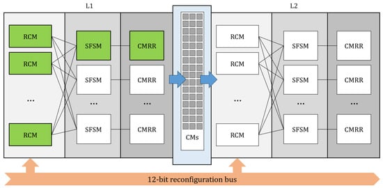
Figure 1.
General structure of the preprocessor. The implementation of a single neuron is marked in green.
We have devised a bespoke TensorFlow model parser for the purpose of transferring pre-trained neural networks into Very Large-Scale Integration (VLSI) circuits, utilizing the SPICE language. We perform model weight extraction and identify the nearest multiplicative factors associated with the RCM component, thereby constructing the preprocessor architecture. The weight values are additionally validated to ensure they are within the preprocessor’s operational range—if their values exceed a given threshold, the corresponding model is discarded and is not further evaluated. In the process of training the classifiers, the parameters from Table 1 are not modified, i.e., the structure of the modules does not change. Only the number of modules and the number of their connections are modified. The next chapter describes the TinyML concept and its use in the learning process. Section 4 presents the analyzed models of the trained networks.
3. TinyML
The evolution of data processing system architectures has resulted in the development of various computing paradigms [26]. The integration of AI technologies with Internet of Things (IoT) technologies [27] has led to the popularization of smart applications, e.g., smart healthcare, smart offices or smart classrooms [28]. Mobile platforms are now not only tools for data processing but also a place for storing data [29]. The convergence of the areas of AI and IoT has led to the creation of new system modeling paradigms: edge intelligence (edge AI) and the artificial intelligence of things (AIoT) [30]. The use of end devices with usually severely limited computing and memory resources requires training models using algorithms that reduce the hardware complexity of specific implementations. The literature presents the test results of the commonly used preprocessing algorithms (e.g., Grubbs Test, Butterworth Filter and DBSCAN) or algorithms for training AI models (e.g., Random Forest and Support Vector Machine) with a manufacturing domain setting [31]. When it comes to neural networks implemented in IoT devices, special attention should be paid to TinyML issues. The author of one of the key review works on TinyML defined this concept as a paradigm that facilitates the launch of machine learning on embedded edge devices [32]. There are many frameworks that support the implementation of TinyML models [32,33]. Most of them are compatible with well-known libraries, such as TensorFlow, ONNX, Caffe, PyTorch, Keras and Scikit-learn. We can identify four main techniques used in the TinyML approach to reduce the complexity of neural networks:
- Quantization—involves reducing the precision of the network parameters;
- Pruning—involves removing unnecessary parameters or entire neurons from the network;
- Fusing—involves reducing the number of parameters by combining them;
- Structure optimization—involves the reduction in the total number of network parameters;
- Hardware acceleration—involves delegating calculations to dedicated hardware modules, e.g., DSP (Digital Signal Processing) blocks.
Applying the above techniques means sacrificing the accuracy and precision of the model. In the IoT, these parameters give way to other important system parameters: power consumption or cost [34]. When it comes to ASICs, tensor processing units (TPUs) are one of the most popular examples of the TinyML paradigm [35]. The approach is also used, for example, in systems for visual processing with a built-in ASIC-based neural co-processor (NCP) [36] or to convert signals acquired from digital Micro-Electro-Mechanical Systems (MEMS) and processed by CMOS circuitry closely coupled with microphones [37].
In the current work, the authors rely mainly on three of the mentioned TinyML methods. The first one, quantization, is imposed by the structure of RCM blocks. Due to the feasibility of the network parameters, their values must have a sufficiently small dispersion. The details of this implementation are described in Section 4. Another technique used is structure optimization to reduce the number of RCM and CM blocks. Additionally, hardware acceleration is used to implement neurons using RCM and SFSM blocks.
4. Neural Network Architecture
The current section presents the implementation details of the trained model. The next subsections describe the dataset used in the training process and the architecture of the neural network in relation to the preprocessor architecture.
The general structure of the edge system for monitoring and processing heart rate signals is shown in Figure 2.
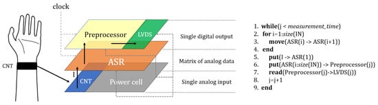
Figure 2.
The concept of a heart rate signal preprocessing system.
One of the most frequently used sensors for heart rate detection is carbon nanotubes (CNTs) integrated with clothes [38]. They provide data in the form of analog currents that can be collected in an analog shift register (ASR). Such registers are based, for example, on second-generation SI memory cells [39]. The algorithm in Figure 2 illustrates the procedure for processing analog data for the subsequent samples collected at time j. The data collection is described in lines 2–5. When the ASR register is full, data in the form of a vector of analog values are fed to the preprocessor (line 6). The size IN of the ASR register is equal to the sampling rate of the heart rate signal. The preprocessor is an analog circuit operating in continuous time. Therefore, the clock signal, which is attached to the preprocessor and to the ASR, only manages the feeding of data. The preprocessor has a differential current output, so it is necessary to convert the output signal into Low-Voltage Differential Signaling (LVDS) (line 7). This conversion is performed using buffer circuits [40]. In this form, the signal can be further analyzed digitally. The power source for all the system modules can be a human energy harvesting cell.
4.1. Dataset
The dataset utilized for training the model is the ECG-ID database, available on PhysioNet [41,42]. The creator of the database is Tatiana Lugovaya [42]. It comprises 310 different electrocardiogram (ECG) recordings collected from 44 male and 46 female participants, totaling 90 individuals aged between 13 and 75 years. Each recording is composed of the following:
- Two ECG signals—one raw and one filtered;
- Ten pairs of annotations, representing R- and T-wave peaks from an automated detector;
- Metadata, such as the basic information about a patient, including the age, gender and recording date.
Furthermore, every recording had a small number of apparent misplacements in the annotations (typically one or two), which were manually rectified. Subsequently, the raw data underwent processing to generate pairs of sampled signal data and binary outcomes. The entire ECG signal was partitioned into windows of a predefined length (window_length), from which a specific number of points (sampling_frequency) were uniformly sampled. A window was labeled as true (indicating the presence of a heartbeat) if it contained a peak. Both the width of the windows and the number of points are hyperparameters that were later optimized. Examples of the ECG signals obtained from three randomly selected patients are shown in Figure 3.
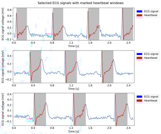
Figure 3.
Sample segments of ECG signals obtained from three randomly selected patients. The red part of the signal and the gray shaded regions represent heartbeat windows.
4.2. Neural Network
While designing the neural network’s structure, we had to consider a trade-off between the performance of the neural network and the physical parameters of the final semiconductor structure. In particular, the parameters of the power consumption, processing speed and surface area of the circuit are important. The latter parameter translates into production costs. A more complex architecture can achieve better accuracy at the cost of an increased number of trainable parameters, resulting in a larger physical device requiring more power. The propagation of signals in a circuit with a larger structure will have a negative impact on its maximum operating frequency. Given the above limitations, the focus was on networks with a single hidden layer. There are many examples in the literature of implementing perceptrons, such as CMOS circuits [10,43,44,45,46].
The standard architecture of the neural networks utilized in this study is as follows:
- Input layer—comprising window_length (8 to 18 inputs);
- Hidden layer with an activation function—comprising 6 to 16 neurons;
- Output layer with an activation function.
The weights of each layer were initialized using the Glorot (Xavier) normal initializer and were subject to regularization by an L2 norm.
The activation function available in the IPcore preprocessor was a slightly modified sigmoidal function. The function implemented in the SFSM module can be approximated by Equation (3).
The activation function returns values in the range of −1 and 1, similar to the hyperbolic tangent; however, the former is substantially steeper. Figure 4 depicts the comparison of a hyperbolic tangent and SFSM activation function.
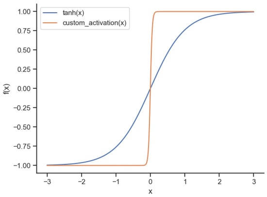
Figure 4.
Comparison of a hyperbolic tangent - and SFSM custom activation function -.
In order to train the neural network, it was imperative to temporarily modify the output of the classifier so that it produced values in the range of 0 and 1. This modification was necessary due to a binary cross-entropy loss function, which assumes its inputs to be within the range of 0 and 1. To achieve this behavior, the transformation according to Equation (4) was applied to the output of the neural network.
Another constraint emerged as a limitation, wherein the RCM module could produce a finite number of multipliers. Each combination of a 12-bit input corresponded to a real value ranging from 0.02 to 1.46 [5]. The training process was carried out with an upper limit of the weight values of 1.5 and no limit on the lower weight values (values below 0.02 were acceptable). Finally, the weights were adjusted to replace each weight with the nearest value producible by the RCM module.
At the end of each epoch, the model was evaluated on a validation test, and the training was stopped if the best validation loss had not improved for the selected number of epochs (usually 10). Following the training phase, the model was evaluated twice on a test set. The first evaluation was performed with unmodified weights, after which the weights were replaced with the closest values producible by the RCM module, and the evaluation was repeated. The next section presents the preprocessor tests for a total of 36 models varying in complexity. The preprocessor was implemented in TSMC 65 nm technology and the results were obtained using the Eldo simulator from Siemens Digital Industries. The simulator uses the SPICE language syntax.
5. Hardware Complexity
The general relationship between the model size and its basic accuracy parameter is illustrated in Figure 5. The smallest models (with the smallest hidden layer) are close to each other regardless of the sampling rate. The spread increases as the complexity of the model increases. The complexity of the model itself does not clearly have a positive effect on accuracy. However, a beneficial effect on accuracy of increasing the sampling rate can be observed.
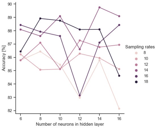
Figure 5.
Accuracy obtained according to combinations of common sampling frequency and hidden layer size.
The analog implementation of the trained model entails a loss of the original accuracy due to parameter scatter. Figure 6 shows this accuracy drop after model implementation. Scores greater than 0 represent configurations for which the preprocessor performed better than the corresponding neural network. The accuracy spread is of the order of ±6%. However, it is noteworthy that the deterioration is only observed for the largest architectures. Paradoxically, for smaller architectures, the analog implementation improves the accuracy slightly. This does not seem to be accidental, as there is a positive inverse correlation between the size of the input layer (IN) and the improvement in the accuracy rate (ACC). According to the data depicted in Figure 7, a notable decrement in the recall score is observed in the context of the 16-neuron implementation. In Figure 8, we plot the relationship between the model size and F1 score of the VLSI implementation. Figure 9 reveals an absence of noticeable trends or statistically significant patterns, indicating a lack of clear associations among the variables under investigation.
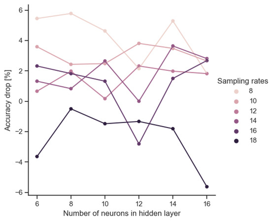
Figure 6.
Decrease in accuracy between the model and the VLSI implementation.
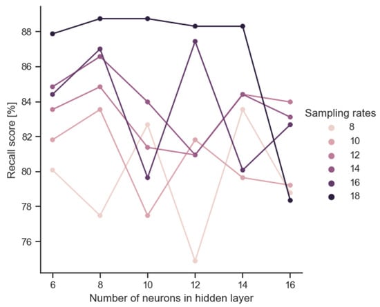
Figure 7.
Evaluating VLSI implementation performance with recall score.
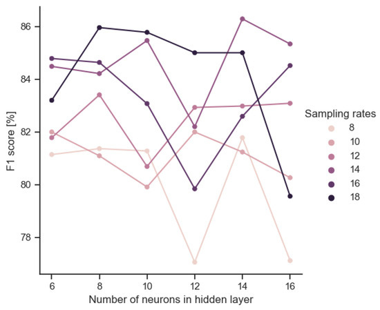
Figure 8.
F1 score of VLSI implementation obtained according to combinations of common sampling frequency and hidden layer size.
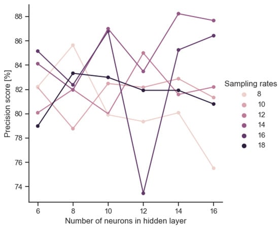
Figure 9.
Evaluating VLSI implementation precision across scenarios.
The results for all the metrics are presented in Table 2. To maintain brevity, only the best architecture for each sampling rate value is featured in the table. The architecture of a sampling rate of 14 and a hidden layer size of 14 turns out to perform best on 3 out of 4 metrics, which we consider to be the best architecture overall.
Further analyses of the parameter relations are based on the comparison of different configurations of the sizes of the input (IN) and hidden (HL) layers or the total number of model parameters (NP). The results of the subsequent tests show the influence of the model complexity on the parameters of the semiconductor structure: active surface (Figure 10), maximum power consumption (Figure 11) and maximum processing speed (Figure 12).
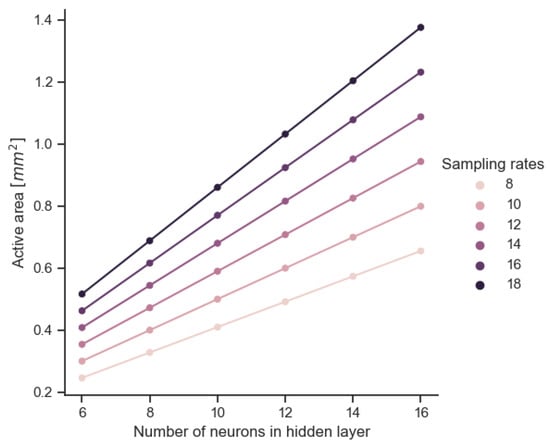
Figure 10.
Active area of VLSI implementation obtained according to combinations of common sampling frequency and hidden layer size.
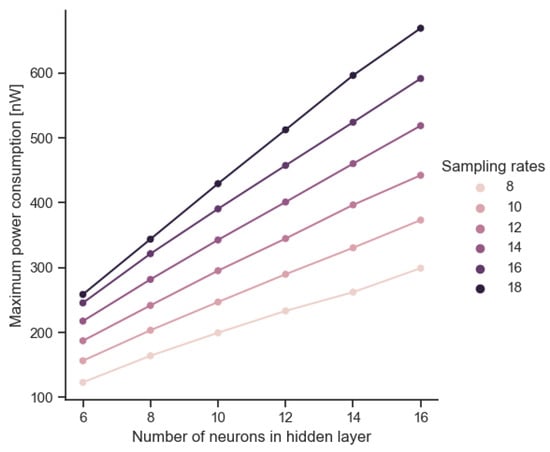
Figure 11.
Maximum power consumption of VLSI implementation obtained according to combinations of common sampling frequency and hidden layer size.
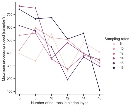
Figure 12.
Maximum processing speed of VLSI implementation obtained according to combinations of common sampling frequency and hidden layer size.
Table 2.
Aggregated results for each sampling rate. Each row corresponds to the best architecture for a given sampling rate value. The highest metric values and the indication of the best model are marked in bold.
Table 2.
Aggregated results for each sampling rate. Each row corresponds to the best architecture for a given sampling rate value. The highest metric values and the indication of the best model are marked in bold.
| Sampling Rate | Hidden Neurons | Accuracy | F1 | Precision | Recall |
|---|---|---|---|---|---|
| 8 | 14 | 0.857 | 0.817 | 0.800 | 0.835 |
| 10 | 12 | 0.862 | 0.819 | 0.821 | 0.818 |
| 12 | 8 | 0.871 | 0.834 | 0.820 | 0.848 |
| 14 | 14 | 0.897 | 0.862 | 0.882 | 0.844 |
| 16 | 6 | 0.884 | 0.847 | 0.851 | 0.844 |
| 18 | 8 | 0.889 | 0.859 | 0.833 | 0.887 |
Based on the analyses performed, estimates of the parameter dependencies are determined and collected in Table 3 (in terms of the area parameter), Table 4 (in terms of the power parameter) and Table 5 (in terms of the frequency parameter). The estimates presented in the tables are approximating functions obtained using the least squares method. The forms of the approximating functions are determined by minimizing the objective function defined by Equation (5), where is the sought approximating function depending on the variable, is the value read from the analyses for the variable and f is the objective function depending on the optimized coefficients .
The variables , are the model parameters (e.g., the size of the input layer (IN), the size of the hidden layer (HL) or the number of all network parameters (NP)). The number of coefficients . depends on the result of the optimization process, although it is worth ensuring that their number is as small as possible so that the form of the approximating function is as simple as possible. For the simplest, i.e., linear approximation function, the objective function may have the form as in Equation (6), where the sum of squares is calculated for all architectures, i.e., according to the sizes of the input layer IN and hidden layer HL.
In some cases, the approximation function may depend on more than one model parameter. This was the case of estimating the maximum operating frequency (visible in Table 5). Then, the additional model parameter is taken as the objective function variable, as in Equation (7).
The optimized coefficients c in the functions are typical for the technology used. All estimating functions accept model parameters as variables and thus allow for the estimation of circuit parameters at the model training stage, i.e., before its transistor implementation.
Table 3.
Approximate relationship between model hyperparameters and circuit area.
Table 3.
Approximate relationship between model hyperparameters and circuit area.
| Area (mm) | |
|---|---|
| sampling rates (IN) | |
| number of parameters (NP) | |
| ACC (%) | |
| F1 (%) | |
| recall (%) | |
| precision (%) | |
| Coefficients for 65 nm CMOS technology: | |
| , , , , , , , | |
| , , , , , , , | |
| , , , , , , | |
Table 3 summarizes the dependence of the CMOS preprocessor area on the parameters of the neural network model. The presented relationships allow for the estimation of the final area of the active region. To estimate the relationship with the sampling rates (identical to the size of the input layer (IN)), implementations with the hidden layer size (HL) giving the highest accuracy value are used. This relationship is linear. In practice, this means that increasing the sampling rates by 1 increases the circuit area by another 8 ÷ 10%. Determining a simple relationship with respect to the total number of neurons is quite difficult, because the size of the circuits affects both the input and hidden layers. It is much easier to identify the dependence on the parameter referred to as the number of channels (NC) [47]. This parameter translates directly into the number of parameters (NP) of the trained model. To a close approximation, it can be assumed that the relationship between the active area of the chip and the NP parameter has a polynomial character. This is due to the current processing mode and the need to use current signal replication CMs circuits shown in Figure 1. The number of these circuits increases as the size of the input layer increases. Additionally, the size of these circuits also increases as the number of neurons in the hidden layer increases. For the TSMC 65 nm technology used, each subsequent parameter covers from a 0.003 mm (for the smallest architectures) to 0.006 mm (for the largest architectures) CMOS structure area. Network architectures ranging in size from 8-6-1 to 18-16-1 are used in the analyses. The relationship with the accuracy, F1, recall and precision scores is the least favorable because of an exponential nature in each of the above cases. In practice, this means, for example, that for every 1% increase in the accuracy of the model, the active area of the circuit increases by another 25 ÷ 45%. At the bottom of Table 3, the coefficients values for the TSMC 65 nm technology used in the analyses are collected.
Table 4.
Approximate relationship between model hyperparameters and circuit maximum power consumption.
Table 4.
Approximate relationship between model hyperparameters and circuit maximum power consumption.
| (nW) | |
|---|---|
| sampling rates (IN) | |
| number of parameters (NP) | |
| ACC (%) | |
| F1 (%) | |
| recall (%) | |
| precision (%) | |
| Coefficients for 65 nm CMOS technology: | |
| , , , , , , , | |
| , , , , , , , | |
| , , , , , , | |
Table 4 shows the dependence of the maximum power consumption of the CMOS preprocessor on the parameters of the neural network model. The coefficients of the estimating functions are summarized at the bottom of the table. The relationships are of a similar nature as in the case of previous analyses regarding area occupancy. The relationship shows that increasing sampling rates by 1 results in an increase in power consumption from 9% (for high current sampling) to 33% (for low current sampling). When it comes to increasing the size of the entire neural network, each subsequent model parameter increases the power consumption by a value from 1.78 nW (for a small 8-6-1 architecture) to 2.55 nW (for a large 18-16-1 architecture). Improving the accuracy, F1, recall or precision scores of the model by 1% results in an exponential increase in power consumption. For example, with an ACC below 87%, the increase in power consumption is less than 10% for every 1% ACC. With an ACC in the range of 87–90%, this increase is several percent. With an ACC above 90%, the increase exceeds 30% for each additional 1% ACC. The remaining parameters, F1, recall and precision, have a similarly exponential influence.
The summary of the above analyses is a comparison of the power consumption for individual preprocessor implementations with the efficiency of human energy harvesting cells. This summary is presented in Figure 13. The figure shows the power consumed by a preprocessor with a given area and the power generated by a cell with the same area. The analysis assumes that the cell efficiency is 60 μW/cm [22]. Based on the comparison, it can be concluded that regardless of the complexity of the model, this value is sufficient for the preprocessor to work without an additional power source and without increasing the surface area of the final device.
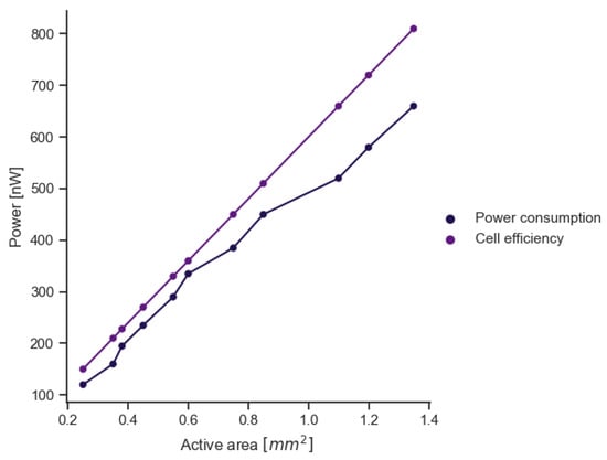
Figure 13.
Comparison of the power consumption of the active area with the efficiency of a human energy harvesting cell.
Table 5 shows the dependence of the processing speed on the IN and NP parameters. These relationships are of a slightly different nature than in previous analyses. Increasing the size of the model mainly results in the widening of the preprocessor layers, but this does not translate into its depth. The relationships of the parameters listed in Table 5 are linear. Sampling rates alone are not sufficient to estimate the maximum processing speed. It is necessary to take into account the HL size of the hidden layer. The relationship shows that increasing the signal sampling by one sample results in a change in the processing speed by approximately −2 ÷ 11% of the current speed depending on the HL width. Deterioration is observed for structures with a wider hidden layer. For small architectures with a narrower hidden layer, this relationship is reversed and may result in an increase in the maximum processing frequency. As for the dependence on NP, each additional model parameter (each weight) means a speed decrease of 1.05 samples/s.
Table 5.
Approximate relationship between model hyperparameters and circuit maximum processing frequency.
Table 5.
Approximate relationship between model hyperparameters and circuit maximum processing frequency.
| (Samples/s) | |
|---|---|
| sampling rates (IN) | |
| number of parameters (NP) | |
| ACC, F1, recall, precision (%) | - |
| Coefficients for 65 nm CMOS technology: | |
| , , , , | |
Unfortunately, there is no visible dependence of the processing speed on the training parameters (ACC, F1, recall and precision). This is confirmed by Figure 14 which illustrates the distribution of the area, power and speed parameters, which shows greater independence of the processing speed from the ACC. The distribution of the points in this analysis is more horizontal than in relation to the area occupied or the power consumed. The distribution for the remaining training parameters (F1, recall and precision) is of a similar nature.
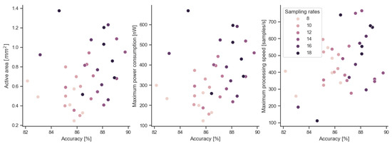
Figure 14.
Dependence of CMOS preprocessor parameters on model accuracy.
The linear, polynomial or exponential dependencies presented in Table 3, Table 4 and Table 5 are characteristic of CMOS circuits operating in the current mode and were also observed by the authors during their previous research based on 180 nm and 350 nm technologies [12,48]. Only the , and parameters are specific to a specific technology. In this work, the authors present analyses based on TSMC 65 nm CMOS technology and the values of the mentioned coefficients refer only to this specific technology. Similarly, Table 6 summarizes the cost estimates for the semiconductor implementation of model parameters and these values are valid only for previously mentioned technology and when using current and weak inversion modes. The table presents the increase in, e.g., the maximum power consumption derived from the preprocessor, with respect to, e.g., a 1% improvement in accuracy. The parameters are divided according to two stages of model training: fast training (initial training with lower ACC, F1, recall and precision values) and precise training (training the model with optimization of higher values of these parameters). Comparing the costs of the model’s various parameters leads to a conclusion that the cost of improving the overall model’s performance is greater for precise training. For example, the accuracy gain of 1% in relation to the area of the preprocessor for fast training is roughly 10 times lower than for precise training. As shown in Table 3, the relationship between the accuracy and area is exponential, which makes it considerably more expensive to improve the accuracy score for an already optimized, well-performing model. The costs given in the table are a certain simplification of complex relationships and can be used only as a preliminary estimate of the final results of implementing a computing CMOS device.
Table 6.
Costs of implementing model parameters using TSMC 65 nm CMOS technology.
Table 6.
Costs of implementing model parameters using TSMC 65 nm CMOS technology.
| CMOS Structure Parameters | Fast Training | Precise Training |
|---|---|---|
| Area | 0.1 mm/1 sampling rate | 0.1 mm/1 sampling rate |
| 0.003 ÷ 0.006 mm/1 weight | 0.003 ÷ 0.006 mm/1 weight | |
| 0.022 mm/1% ACC | 0.2 mm/1% ACC | |
| 0.021 mm/1% F1 | 0.14 mm/1% F1 | |
| 0.01 mm/1% recall | 0.13 mm/1% recall | |
| 0.004 mm/1% precision | 0.15 mm/1% precision | |
| 50 nW/1 sampling rate | 50 nW/1 sampling rate | |
| 1.78 ÷ 2.55 nW/1 weight | 1.78 ÷ 2.55 nW/1 weight | |
| 4.3 ÷ 10.3 nW/1% ACC | 25.7 ÷ 105 nW/1% ACC | |
| 6.5 ÷ 11.2 nW/1% F1 | 44.2 ÷ 112 nW/1% F1 | |
| 0.8 ÷ 3.1 nW/1% recall | 16.8 ÷ 42.7 nW/1% recall | |
| 0.9 ÷ 3.5 nW/1% precision | 47.1 ÷ 118 nW/1% precision | |
| −37 samples/s/1 sampling rate | −37 samples/s/1 sampling rate | |
| 1.05 samples/s/1 weight | 1.05 samples/s/1 weight |
Finally, let us briefly analyze the limitations of the presented approach to estimating implementation costs. The forms of the presented approximation functions are independent of the technology, but the values of the c coefficients are typical only for a specific technology. This necessitates their designation when technology changes. This work is also limited to circuits operating in the current mode and weak inversion mode. These are indeed some of the most frequently used operating modes in medical applications of nanometer CMOS technology. However, the presented dependencies will not be met for other operating and power supply modes.
6. Conclusions
This work addresses the problem of combining the field of artificial intelligence with the technology of producing edge devices using semiconductors. Based on the reconfigurable architectures operating in the current mode, several dozen sample preprocessors implementing neural networks of various complexity were implemented. Based on the analyses, correlations between the parameters of the trained models and the physical parameters of semiconductor structures were determined. First of all, the complexity of the hardware implementation was determined, which is linear in relation to the size of the analyzed data (sampling rates), polynomial in relation to the size of the neural network and exponential in relation to the hyperparameters of the learning process. Next, analytical methods in the form of simple approximating functions for estimating the costs of implementing specific model parameters in the CMOS structure were proposed. The forms of the approximating functions are independent of technology and allow for a preliminary estimate of the result of the future synthesis of the model as an integrated circuit. This work determines the function coefficients for the selected technology and compares the costs of improving model parameters for two network training scenarios: fast and precise. The use of the presented methods for subsequent process nodes requires only the determination of coefficients characteristic of a given technology. We hope that these approaches along with cost estimation will prove useful when training TinyML class models and will allow you to direct the implementation process according to the right criteria.
Author Contributions
Conceptualization, S.S. (Szymon Szczęsny); methodology, S.S. (Sebastian Szczepaniak); software, P.B., N.M., S.S. (Sebastian Szczepaniak) and K.P.; validation, P.B. and S.S. (Sebastian Szczepaniak); formal analysis, S.S. (Szymon Szczęsny); investigation, P.B. and S.S. (Sebastian Szczepaniak); resources, N.M. and K.P.; data curation, P.B. and S.S. (Sebastian Szczepaniak); writing—original draft preparation, P.B. and S.S. (Szymon Szczęsny); writing—review and editing, P.B. and S.S. (Sebastian Szczepaniak); visualization, P.B.; supervision, S.S. (Szymon Szczęsny); project administration, S.S. (Szymon Szczęsny); funding acquisition, S.S. (Szymon Szczęsny). All authors have read and agreed to the published version of the manuscript.
Funding
This research was supported by the Statutory Activity No. 0311/SBAD/0726 of the Faculty of Computing and Telecommunications at the Poznan University of Technology in Poland.
Institutional Review Board Statement
Not applicable.
Informed Consent Statement
Not applicable.
Data Availability Statement
No new data were created or analyzed in this study. Data sharing is not applicable to this article.
Conflicts of Interest
The authors declare no conflict of interest.
Abbreviations
The following abbreviations are used in this manuscript:
| ACC | Accuracy |
| AIoT | Artificial Intelligence of Things |
| ASIC | Application-Specific Integrated Circuit |
| CM | Current Mirror |
| CMRR | Common Mode Rejection Ratio |
| FPGA | Field-Programmable Gate Arrays |
| HL | Size of the Hidden Layer |
| IN | Size of the Input Layer |
| MEMS | Micro-Electro-Mechanical Systems |
| NC | Number of Channels |
| NCP | Neural Co-Processor |
| RCM | Reconfigurable Current Mirror |
| SFSM | Sigmoidal Function Shaping Module |
| NP | Number of Parameters |
| TPU | Tensor Processing Unit |
| VPU | Video Processing Units |
References
- Raha, A.; Kim, S.K.; Mathaikutty, D.A.; Venkataramanan, G.; Mohapatra, D.; Sung, R.; Chinya, G.N. Design Considerations for Edge Neural Network Accelerators: An Industry Perspective. In Proceedings of the 2021 34th International Conference on VLSI Design and 2021 20th International Conference on Embedded Systems (VLSID), Guwahati, India, 20–24 February 2021; pp. 328–333. [Google Scholar] [CrossRef]
- Lu, Y.C.; Chen, C.W.; Pu, C.C.; Lin, Y.T.; Jhan, J.K.; Liang, S.P.; Chiueh, H. An 176.3 GOPs Object Detection CNN Accelerator Emulated in a 28nm CMOS Technology. In Proceedings of the 2021 IEEE 3rd International Conference on Artificial Intelligence Circuits and Systems (AICAS), Washington, DC, USA, 6–9 June 2021; pp. 1–4. [Google Scholar] [CrossRef]
- Piro, F.; Rinella, G.A.; Andronic, A.; Antonelli, M.; Aresti, M.; Baccomi, R.; Villani, A. A Compact Front-End Circuit for a Monolithic Sensor in a 65 nm CMOS Imaging Technology. IEEE Trans. Nucl. Sci. 2023, 70, 2191–2200. [Google Scholar] [CrossRef]
- Nguyen-Hoang, D.-T.; Ma, K.-M.; Le, D.-L.; Thai, H.-H.; Cao, T.-B.-T.; Le, D.-H. Implementation of a 32-Bit RISC-V Processor with Cryptography Accelerators on FPGA and ASIC. In Proceedings of the 2022 IEEE Ninth International Conference on Communications and Electronics (ICCE), Nha Trang, Vietnam, 27–29 July 2022; pp. 219–224. [Google Scholar] [CrossRef]
- Naumowicz, M.; Pietrzak, P.; Szczęsny, S.; Huderek, D. CMOS Perceptron for Vesicle Fusion Classification. Electronics 2022, 11, 843. [Google Scholar] [CrossRef]
- Forouhi, S.; Ghafar-Zadeh, E. Applications of CMOS Devices for the Diagnosis and Control of Infectious Diseases. Micromachines 2020, 11, 1003. [Google Scholar] [CrossRef]
- Perri, L. What’s New in Artificial Intelligence from the 2023 Gartner Hype Cycle. Gartner. 17 August 2023. Available online: https://www.gartner.com/en/articles/what-s-new-in-artificial-intelligence-from-the-2023-gartner-hype-cycle (accessed on 20 September 2023).
- Available online: https://www.pewresearch.org/science/2023/02/15/public-awareness-of-artificial-intelligence-in-everyday-activities/ (accessed on 2 September 2023).
- Du, Y.; Du, L.; Gu, X.; Du, J.; Wang, X.S.; Hu, B.; Chang, M.C.F. An Analog Neural Network Computing Engine Using CMOS-Compatible Charge-Trap-Transistor (CTT). IEEE Trans. -Comput.-Aided Des. Integr. Circuits Syst. 2019, 38, 1811–1819. [Google Scholar] [CrossRef]
- Medina-Santiago, A.; Hernández-Gracidas, C.A.; Morales-Rosales, L.A.; Algredo-Badillo, I.; Amador García, M.; Orozco Torres, J.A. CMOS Implementation of ANNs Based on Analog Optimization of N-Dimensional Objective Functions. Sensors 2021, 21, 7071. [Google Scholar] [CrossRef]
- Mohamed, A.R.; Qi, L.; Wang, G. A power-efficient and re-configurable analog artificial neural network classifier. Microelectron. J. 2021, 111, 105022. [Google Scholar] [CrossRef]
- Szczęsny, S. High Speed and Low Sensitive Current-Mode CMOS Perceptron. Microelectron. Eng. 2016, 165, 41–51. [Google Scholar] [CrossRef]
- Lee, M.H.; Yoon, H.R.; Song, H.B. A real-time automated arrhythmia detection system. In Proceedings of the Annual International Conference of the IEEE Engineering in Medicine and Biology Society, New Orleans, LA, USA, 4–7 November 1988; Volume 3, pp. 1470–1471. [Google Scholar] [CrossRef]
- Masuda, H.; Okada, S.; Shiozawa, N.; Makikawa, M.; Goto, D. The Estimation of Circadian Rhythm Using Smart Wear. In Proceedings of the 2020 42nd Annual International Conference of the IEEE Engineering in Medicine & Biology Society (EMBC), Montreal, QC, Canada, 20–24 July 2020; pp. 4239–4242. [Google Scholar] [CrossRef]
- Lee, M.Y.; Yu, S.N. Improving discriminality in heart rate variability analysis using simple artifact and trend removal preprocessors. In Proceedings of the 2010 Annual International Conference of the IEEE Engineering in Medicine and Biology, Buenos Aires, Argentina, 31 August–4 September 2010; pp. 4574–4577. [Google Scholar] [CrossRef]
- Chatterjee, S.; Pun, K.; Nebojša, S.; Tsividis, Y.; Kinget, P. Analog Circuit Design Techniques at 0.5 V; Analog Circuits and Signal Processing; Springer: New York, NY, USA, 2007. [Google Scholar]
- Comer, D.J.; Comer, D.T. Operation of analog MOS circuits in the weak or moderate inversion region. IEEE Trans. Educ. 2004, 47, 430–435. [Google Scholar] [CrossRef]
- Harrison, R. MOSFET Operation in Weak and Moderate Inversion, EE5720; University of Utah: Salt Lake City, UT, USA, 2014. [Google Scholar]
- Manolov, E.D. Design of CMOS Analog Circuits in Subthreshold Region of Operation. In Proceedings of the 2018 IEEE XXVII International Scientific Conference Electronics-ET, Sozopol, Bulgaria, 13–15 September 2018; pp. 1–4. [Google Scholar]
- Aditya, R.; Sarkel, S.; Pandit, S. Comparative Study of Doublet OTA Circuit Topologies Operating in Weak Inversion Mode for Low Power Analog IC Applications. In Proceedings of the 2020 IEEE VLSI Device Circuit and System (VLSI DCS), Kolkata, India, 18–19 July 2020; pp. 74–78. [Google Scholar]
- Szczęsny, S. 0.3 V 2.5 nW per Channel Current-Mode CMOS Perceptron for Biomedical Signal Processing in Amperometry. IEEE Sens. J. 2017, 17, 5399–5409. [Google Scholar] [CrossRef]
- Zou, C.Y.; Lin, B.; Zhou, L. Recent progress in human body energy harvesting for smart bioelectronic system. Fundam. Res. 2021, 1, 364–382. [Google Scholar] [CrossRef]
- Wang, C.-C.; Tolentino, L.K.S.; Chen, P.-C.; Hizon, J.R.E.; Yen, C.-K.; Pan, C.-T.; Hsueh, Y.-H. A 40-nm CMOS Piezoelectric Energy Harvesting IC for Wearable Biomedical Applications. Electronics 2021, 10, 649. [Google Scholar] [CrossRef]
- Giustolisi, G.; Palmisano, G.; Palumbo, G. CMRR frequency response of CMOS operational transconductance amplifiers. IEEE Trans. Instrum. Meas. 2000, 49, 137–143. [Google Scholar] [CrossRef]
- Tzschoppe, C.; Jörges, U.; Richter, A.; Lindner, B.; Ellinger, F. Theory and design of advanced CMOS current mirrors. In Proceedings of the 2015 SBMO/IEEE MTT-S International Microwave and Optoelectronics Conference (IMOC), Porto de Galinhas, Brazil, 3–6 November 2015; pp. 1–5. [Google Scholar]
- Donno, M.D.; Tange, K.; Dragoni, N. Foundations and Evolution of Modern Computing Paradigms: Cloud, IoT, Edge, and Fog. IEEE Access 2019, 7, 150936–150948. [Google Scholar] [CrossRef]
- Alahi, M.E.E.; Sukkuea, A.; Tina, F.W.; Nag, A.; Kurdthongmee, W.; Suwannarat, K.; Mukhopadhyay, S.C. Integration of IoT-Enabled Technologies and Artificial Intelligence (AI) for Smart City Scenario: Recent Advancements and Future Trends. Sensors 2023, 23, 5206. [Google Scholar] [CrossRef]
- Kakandwar, S.; Bhushan, B.; Kumar, A. Chapter 3-Integrated machine learning techniques for preserving privacy in Internet of Things (IoT) systems. In Cognitive Data Science in Sustainable Computing, Blockchain Technology Solutions for the Security of IoT-Based Healthcare Systems; Bhushan, B., Sharma, S.K., Saračević, M., Boulmakoul, A., Eds.; Academic Press: New York, NY, USA, 2023; pp. 45–75. [Google Scholar]
- Khatoon, N.; Dilshad, N.; Song, J. Analysis of Use Cases Enabling AI/ML to IOT Service Platforms. In Proceedings of the 2022 13th International Conference on Information and Communication Technology Convergence (ICTC), Jeju Island, Republic of Korea, 19–21 October 2022; pp. 1431–1436. [Google Scholar]
- Available online: https://camad2023.ieee-camad.org/edge-intelligence-and-artificial-intelligence-things-edge-ai-aiot (accessed on 13 September 2023).
- Rupprecht, B.; Hujo, D.; Vogel-Heuser, B. Performance Evaluation of AI Algorithms on Heterogeneous Edge Devices for Manufacturing. In Proceedings of the 2022 IEEE 18th International Conference on Automation Science and Engineering (CASE), Mexico City, Mexico, 22–26 August 2022; pp. 2132–2139. [Google Scholar]
- Ray, P.P. A review on TinyML: State-of-the-art and prospects. J. King Saud Univ.-Comput. Inf. Sci. 2022, 34, 1595–1623. [Google Scholar] [CrossRef]
- Sanchez-Iborra, R.; Skarmeta, A.F. Tinyml-enabled frugal smart objects: Challenges and opportunities. IEEE Circ. Syst. Mag. 2020, 20, 4–18. [Google Scholar] [CrossRef]
- Zhang, Y.; Wijerathne, D.; Li, Z.; Mitra, T. Power-Performance Characterization of TinyML Systems. In Proceedings of the 2022 IEEE 40th International Conference on Computer Design (ICCD), Olympic Valley, CA, USA, 23–26 October 2022; pp. 644–651. [Google Scholar]
- Abadade, Y.; Temouden, A.; Bamoumen, H.; Benamar, N.; Chtouki, Y.; Hafid, A.S. A Comprehensive Survey on TinyML. IEEE Access 2023, 11, 96892–96922. [Google Scholar] [CrossRef]
- Xu, K.; Zhang, H.; Li, Y.; Lai, Y.Z.R. An Ultra-low Power TinyML System for Real-time Visual Processing at Edge. arXiv 2022, arXiv:2207.04663. [Google Scholar] [CrossRef]
- Vitolo, P.; Liguori, R.; Di Benedetto, L.; Rubino, A.; Pau, D.; Licciardo, G.D. A New NN-Based Approach to In-Sensor PDM-to-PCM Conversion for Ultra TinyML KWS. Trans. Circuits Syst. II Express Briefs 2022, 70, 1595–1599. [Google Scholar] [CrossRef]
- Biochemical Sensors Using Carbon Nanotube Arrays. U.S. Patent 7,939,734, 10 May 2011.
- Handkiewicz, A. Mixed-Signal Systems: A Guide to CMOS Cicuit Design; Wiley: New York, NY, USA, 2002. [Google Scholar]
- Śniatała, P.; Naumowicz, M.; Handkiewicz, A.; Szczęsny, S.; Melo, J.L.; Paulino, N.; Goes, J. Current mode sigma-delta modulator designed with the help of transistor’s size optimization tool. Bull. Polish Acad. Sci. Tech. Sci. 2015, 63, 919–922. [Google Scholar] [CrossRef]
- Goldberger, A.; Amaral, L.; Glass, L.; Hausdorff, J.; Ivanov, P.C.; Mark, R.; Stanley, H.E. PhysioBank, PhysioToolkit, and PhysioNet: Components of a new research resource for complex physiologic signals. Circulation 2000, 101, e215–e220. [Google Scholar] [CrossRef]
- Lugovaya, T.S. Biometric Human Identification Based on Electrocardiogram. Master’s Thesis, Faculty of Computing Technologies and Informatics, Electrotechnical University LETI, Saint-Petersburg, Russian, June 2005. [Google Scholar] [CrossRef]
- Geng, C.; Sun, Q.; Nakatake, S. An Analog CMOS Implementation for Multi-layer Perceptron with ReLU Activation. In Proceedings of the 2020 9th International Conference on Modern Circuits and Systems Technologies (MOCAST), Bremen, Germany, 11–13 May 2020; pp. 1–6. [Google Scholar]
- Amarnath, G.; Akula, S.; Vinod, A. Employing Analog Circuits by Neural-Network based Multi-Layer-Perceptron. In Proceedings of the 2021 Fourth International Conference on Electrical, Computer and Communication Technologies (ICECCT), Erode, India, 15–17 September 2021; pp. 1–3. [Google Scholar]
- Geng, C.; Sun, Q.; Nakatake, S. Implementation of Analog Perceptron as an Essential Element of Configurable Neural Networks. Sensors 2020, 20, 4222. [Google Scholar] [CrossRef] [PubMed]
- Dix, J.; Holleman, J.; Blalock, B.J. Programmable Energy-Efficient Analog Multilayer Perceptron Architecture Suitable for Future Expansion to Hardware Accelerators. J. Low Power Electron. Appl. 2023, 13, 47. [Google Scholar] [CrossRef]
- Talaśka, T.; Kolasa, M.; Długosz, R.; Pedrycz, W. Analog programmable distance calculation circuit for winner takes all neural network realized in the CMOS technology. IEEE Trans. Neural Netw. Learn. Syst. 2016, 27, 661–673. [Google Scholar] [CrossRef] [PubMed]
- Handkiewicz, A.; Szczęsny, S.; Naumowicz, M.; Katarzyński, P.; Melosik, M.; Śniatała, P. Marek Kropidłowski, SI-Studio, a layout generator of current mode circuits. Expert Syst. Appl. 2015, 42, 3205–3218. [Google Scholar] [CrossRef]
Disclaimer/Publisher’s Note: The statements, opinions and data contained in all publications are solely those of the individual author(s) and contributor(s) and not of MDPI and/or the editor(s). MDPI and/or the editor(s) disclaim responsibility for any injury to people or property resulting from any ideas, methods, instructions or products referred to in the content. |
© 2023 by the authors. Licensee MDPI, Basel, Switzerland. This article is an open access article distributed under the terms and conditions of the Creative Commons Attribution (CC BY) license (https://creativecommons.org/licenses/by/4.0/).