1. Introduction
With the development of automobile technology, many electronic control units (ECUs) are being connected to vehicles. In particular, automated driving systems (ADSs) and advanced driver assistance systems (ADASs) have significantly increased the number and performance of cameras and displays in vehicles [
1,
2]. Accordingly, a high transmission rate of 1 to 16 Gbps is currently required, and it is expected that the data transmission rate will be increased to 100 Gbps in 2025 [
3,
4]. However, existing in-vehicle networks such as controller area networks (CANs), local interconnected networks (LINs), and flexray and media-oriented system transport (MOST) have the problem of the transmission rate being limited to 1∼150 Mbps [
5].
Automotive Ethernet and Serializer/Deserializer (SerDes) physical (PHY) layers have been widely studied as new PHY layers for in-vehicle networks. Besten et al. [
6] emphasized that new PHY technology is needed as a data streaming solution for high-resolution sensors rather than the Ethernet. Ahmadi et al. [
7] gave an example of the data transmission speed required for automobiles and talked about the need for SerDes transmission for asymmetric data transmission, such as cameras and displays. Kraemer [
8] introduced conferences held for Automotive Ethernet and the development of standards, including 802.3 (Ethernet) and 802.1 (Mac bridge). Hank et al. [
9] explained the importance of Ethernet and PHY interfaces that provide scalability and flexibility for next-generation in-vehicle networking. Ashjaei et al. [
10] introduced the Ethernet as a high-bandwidth, low-latency data transmission technology for future autonomous vehicles. Law [
11] introduced a proposed standard with multi-gigabit optical Ethernet for automobiles. The automotive Ethernet is a full-duplex method, which is helpful in the backbone network configuration but has low efficiency in asymmetric connections such as cameras and displays [
12,
13,
14]. Therefore, the need for automotive SerDes PHY, which is a high-speed asymmetric solution, has increased. Gigabit multimedia serial links (GMSLs) [
15], flat panel display links (FPD-Links) [
16] and automotive pixel links (APIXs) [
17] are currently used automotive SerDes, but they have a transmission rate of 4∼6 Gbps and are proprietary technologies.
The automotive SerDes Alliance (ASA) and A-PHY interfaces were proposed as new open standards to meet the demand for higher transmission speeds [
18,
19]. ASA and A-PHY interfaces are similar automotive SerDes standards that support transmission rates of 2∼16 Gbps. However, the difference is that the ASA interface uses forward error correction, and the A-PHY interface uses retransmission-based error correction. Among them, A-PHY has already been adopted as an IEEE standard [
19], and development of the next version supporting a transmission rate of 32 Gbps is being prepared [
20].
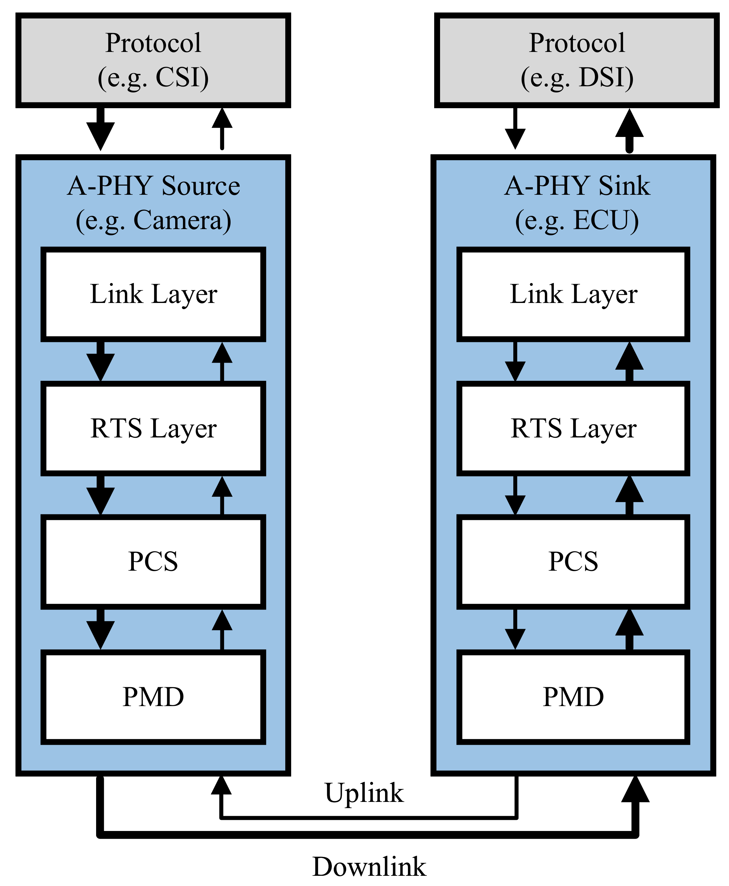
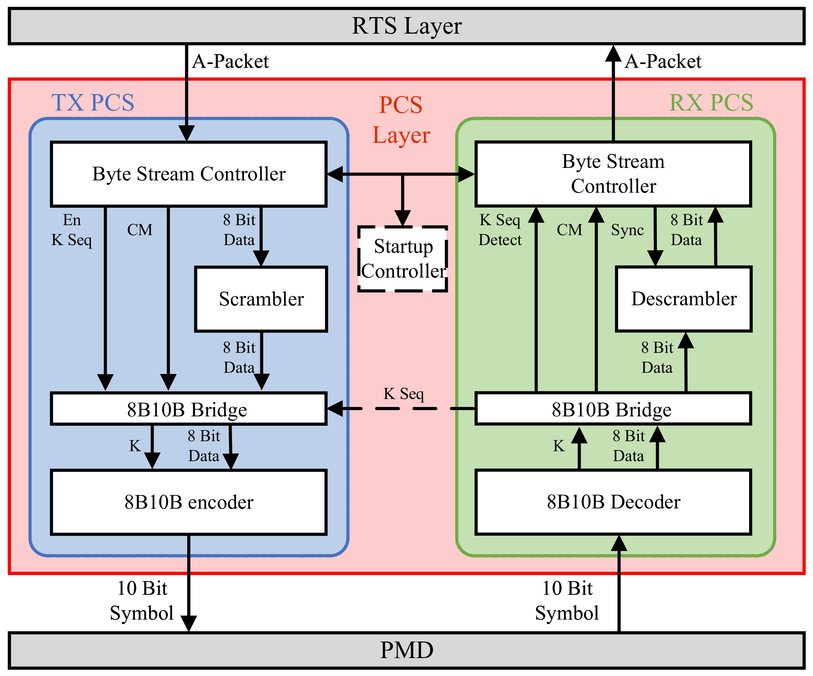
The A-PHY interface is a standard created by Mobile Industry Processor Interface (MIPI), which has created a physical level retransmission (RTS) scheme to obtain noise immunity in noisy automotive environments [
19]. RTS is performed in the RTS layer, which is a new physical layer of A-PHY, and the A-PHY interface offers a low packet error rate of 10
using RTS [
21,
22].
In this paper, we propose designing and implementing a detailed architecture for the RTS layer presented in the standard A-PHY interface in an FPGA and an ASIC. The contributions of this paper are as follows:
Based on the RTS specification of the A-PHY interface standard, the detailed structure of the RTS layer, including the transmitter and receiver, was proposed and verified. More specifically, we presented the hardware architecture of the MC (message counter) handler, scheduler, delay, and CRC updater specified in the RTS layer of the A-PHY interface.
The A-PHY interface, including the RTS layer, was implemented and verified on FPGA. As a result of implementation on the Xilinx KC705 board, 3924 LUTs, 2019 registers, and 132 block memories were used, and the maximum operating speed was confirmed to be 200 MHz.
The RTS layer of the A-PHY interface was implemented as an ASIC using the Synopsys SAED 28 nm process. As a result of the implementation, it was confirmed that the number of logic gates used was 25 K, the chip area was 0.40 mm, and the maximum operating speed was 200 MHz.
The rest of this paper is organized as follows. In
Section 2, the A-PHY interface standard is described.
Section 3 presents the structure of the proposed RTS layer.
Section 4 introduces the verification environment of the A-PHY interface. Furthermore, the proposed RTS hardware architecture of the A-PHY interface is validated via register transfer level (RTL) simulations, accompanied by the outcomes of field programmable gate array (FPGA) verification and application-specific integrated circuit (ASIC) implementation. Finally, we conclude this work, and future research is discussed in
Section 5.
3. Proposed RTS Layer
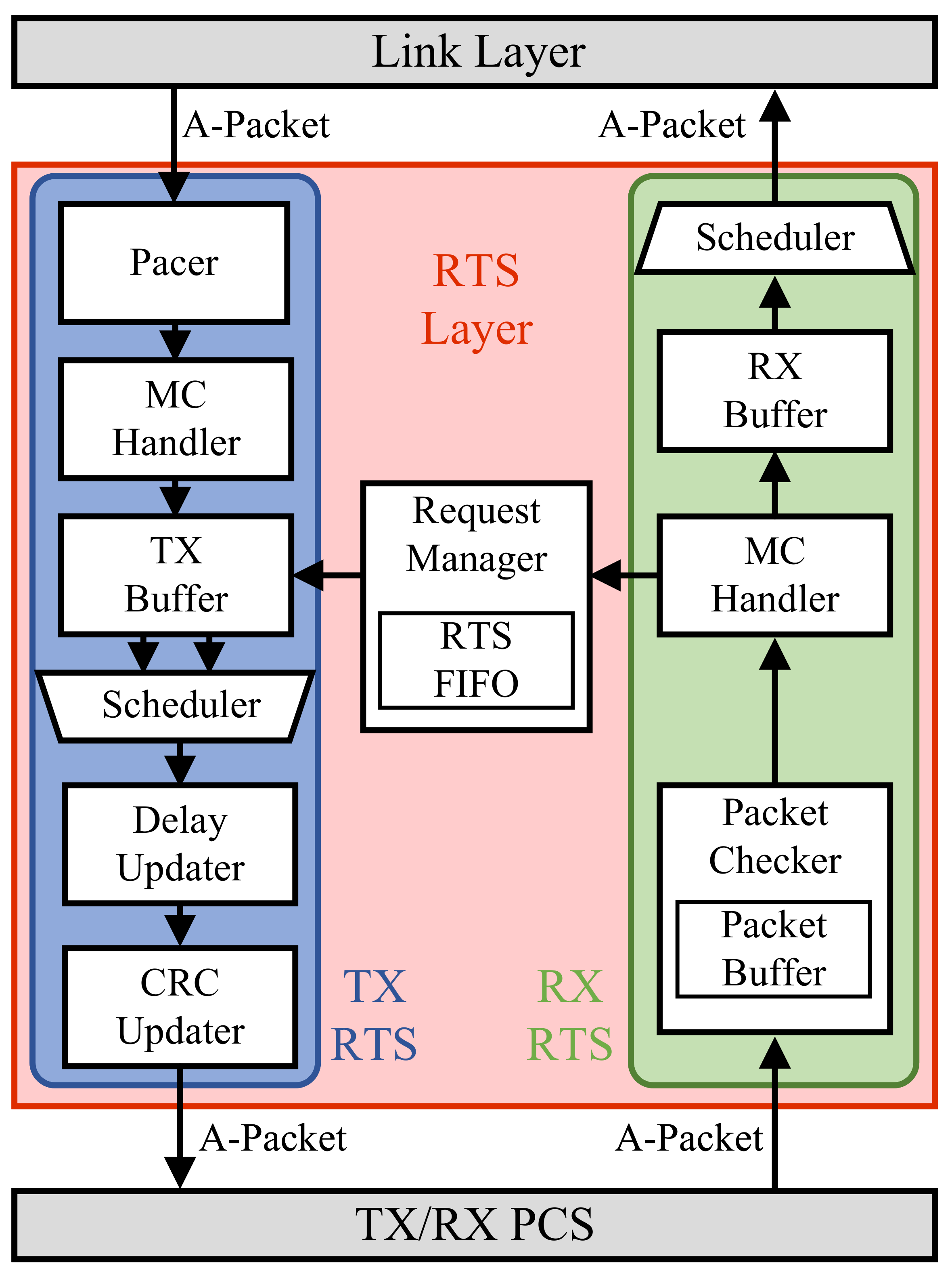
The proposed RTS layer of the A-PHY interface consists of TX RTS, RX RTS, and a request generator, as shown in
Figure 7. TX RTS is configured to store the A-Packet to be transmitted for RTS and insert the CRC, message counter (MC), and delay time in PHY fields into the A-Packet. Conversely, the architecture of RX RTS is designed to evaluate the CRC, MC, and delay fields, subsequently issuing RTS requests in the event of discrepancies. In conclusion, A-PHY, characterized as an asymmetric transmission architecture, exhibits disparate transmission rates between TX RTS and RX RTS. As a result, the Request Manager module facilitates clock domain crossing of the retransmission (RTS) request signal utilizing FIFO mechanisms. In the subsequent subsections, the methodologies for implementing TX RTS and RX RTS, as proposed in this study, are presented comprehensively.
3.1. TX RTS Architecture
As shown in
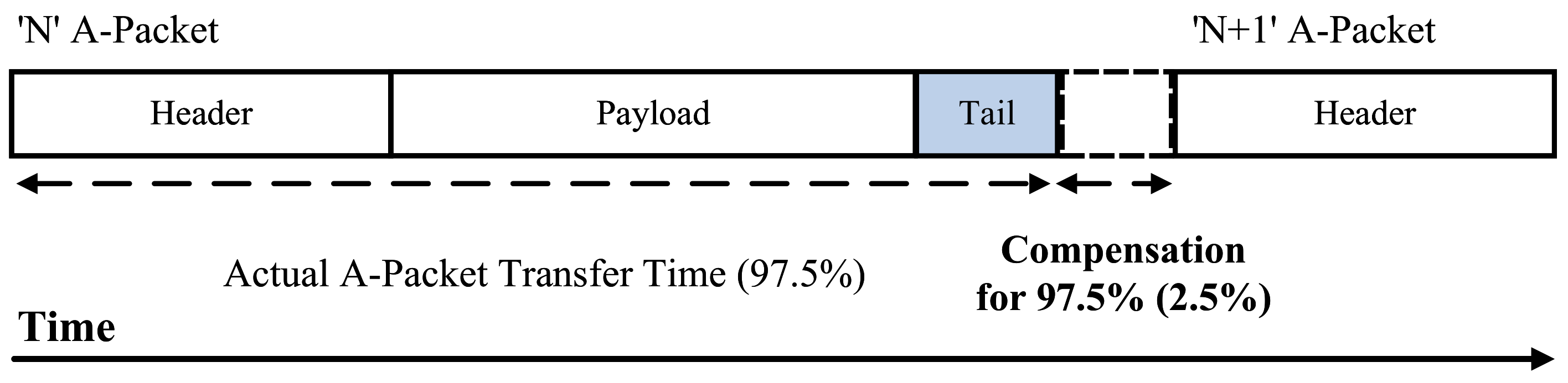
Figure 7, the structure of TX RTS is composed of several modules: a Pacer, a TX MC handler, a TX buffer, a TX scheduler, a delay, and a CRC updater. The Pacer module governs the transmission of A-Packets from the data link layer to the physical layer, accommodating the overhead and retransmission introduced based on the control signal and the 8B10B encoding inherent in the A-PHY interface. The overhead for a single transmission encompasses an 8-byte header, a 4-byte tail, an additional 2 bytes for control in the PCS, and finally, the 8B10B encoding applied to every byte. Given that each byte is transformed into a 10-bit symbol due to the 8B10B encoding, the transmission duration for each byte equates to 10/GearBW (bps). Consequently, the actual transmission time for an A-Packet can be deduced using Equation (
3).
In the given scenario, a minimum of 2.5% of the physical transmission rate is mandated for retransmission, which implies that a maximum of 97.5% of the rate is available for the original A-Packet transmission. Consequently, the Pacer module modulates the A-Packet transmission from the data link layer, ascertaining the compensatory time such that the actual A-Packet transmission time remains confined to 97.5% of the physical transmission capacity, as depicted in
Figure 8.
The computation of the compensatory time by the Pacer module leverages the fact that the proportion of the original A-Packet within 97.5% of the physical transmission volume is represented as a 39/40 ratio. During the transmission of the original A-Packet, a value of 40 is appended to each byte, and 39 is deducted from all bytes, resulting in a negative sum. This process ensures a minimum compensation time of 2.5%, preparing for the subsequent A-Packet transmission. Therefore, the Pacer module’s architecture is formulated to produce a compensation time that spans between a minimum of 2.79% and a maximum of 6.25% of the physical transmission volume, contingent upon the payload’s length.
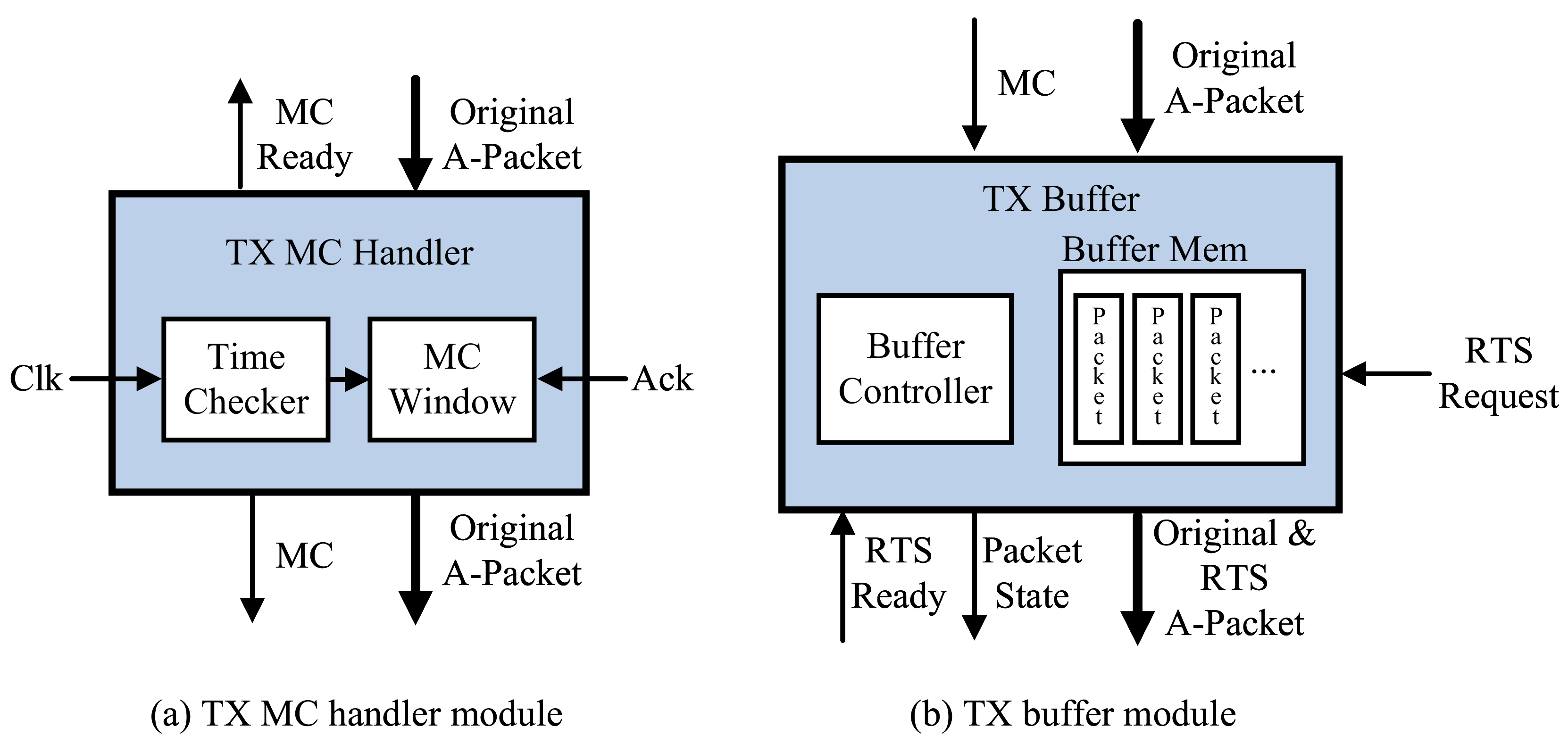
The TX message counter (MC) handler module assigns sequential 8-bit values to the MC, which is the PHY field of the A-Packet header. Currently, the MC is a standard for each A-Packet in each A-PHY interface and is used to detect omissions between transmitted A-Packets or in retransmission.
Figure 9a shows the block diagram of the proposed TX MC handler. MC values are managed through the MC window. When a new A-Packet is transmitted, the maximum value of the MC window increases, and the maximum value of the MC window is given to the A-Packet. Conversely, when the A-Packet is stored for a long time when an acknowledge (ACK) signal is received or recorded through a time checker, the minimum value of the MC window increases. The MC window is designed to control the TX buffer so that it does not become full, and if the buffer is full, it sends a signal to the Pacer so that it does not receive a new A-Packet. At this time, the maximum size of the MC window in the downlink is 128, and in the uplink, it is designed to have a maximum size of 16.
The TX buffer stores the A-Packet being transmitted for retransmission.
Figure 9b shows a block diagram of the proposed TX buffer consisting of a controller and memory. The controller stores and reads the A-Packet’s MC as the address. The memory size is determined according to the maximum size of the MC window. The TX scheduler determines the transmission priority between the original A-Packet and the retransmitted A-Packet. Generally, the priority of a retransmitted A-Packet is higher than that of the original A-Packet, but if there has already been a delay in the transmission of the original A-Packet due to retransmission, the transmission of the original A-Packet is given priority. Therefore, the TX scheduler receives the status of the A-Packet from the TX buffer and transmits the retransmitted A-Packet when there is no problem.
The delay updater module inserts the transmission delay time in the RTS layer, including retransmission, into the Delay field of the PHY field of the A-Packet header. The transmission delay time is calculated using the time difference between the transmission time in the delay updater based on the storage time for each A-Packet recorded in the MC handler. As shown in Equation (
4), the transmission delay time is divided into units to be inserted into the header and converted into a 7-bit normalized RTS layer delay time. The delay time is inserted into the 8-bit header, and the remaining 1-bit indicates the original A-Packet.
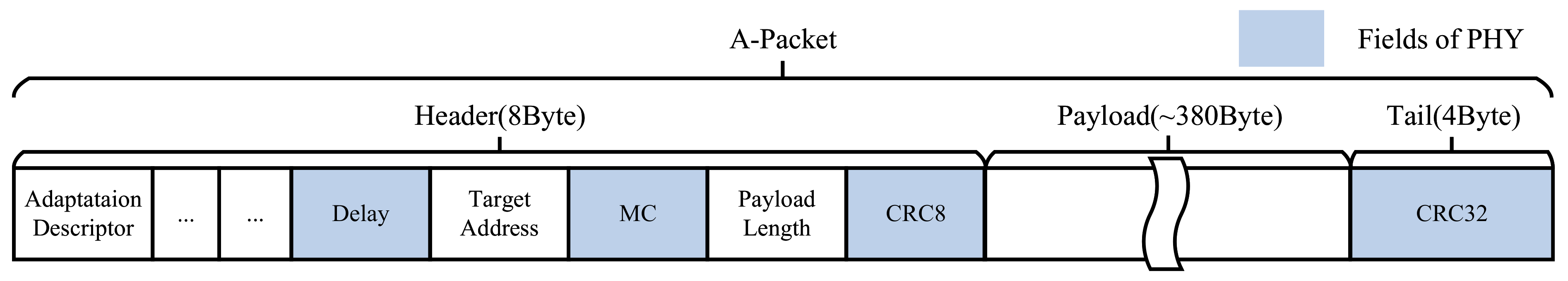
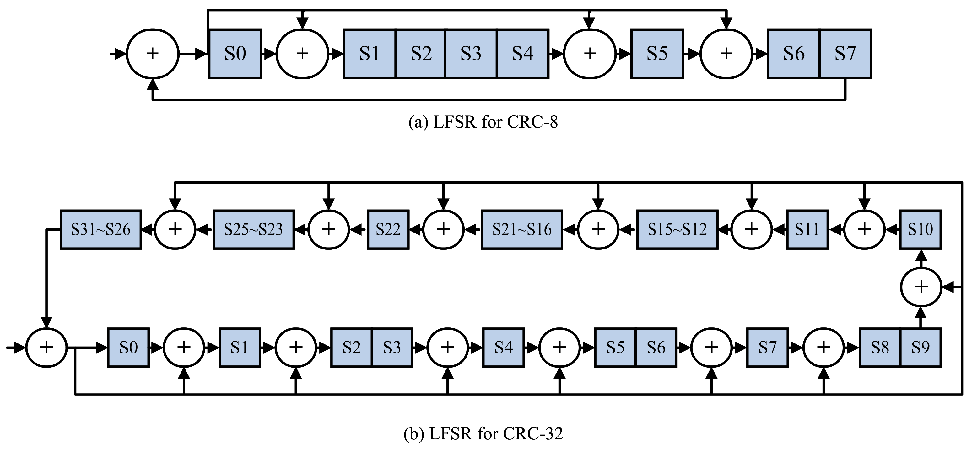
The cyclic redundancy check (CRC) updater is a module that generates a CRC to detect errors and inserts it into the PHY field of the A-Packet header and tail. The CRC is created and transmitted based on the transmitted data, and the receiving side generates a CRC again based on the transmitted data and compares it with the transmitted CRC to detect errors. Currently, the header’s CRC is an 8-bit CRC-8, which detects only header errors, and the tail’s CRC is a 32-bit CRC, which detects payload errors.
Figure 10a is the linear feedback shift register (LFSR) for the CRC used to generate CRC-8, and the polynomial used in the CRC is Equation (
5). Similarly, the CRC LFSR and polynomial used to generate CRC-32 are shown in
Figure 10b and Equation (
6). The LFSR shown in
Figure 10a,b has a structure in which only one bit moves for each clock. In this paper, since 8 bits are processed every clock, we designed a parallel LFSR in which 8 bits are moved every clock while satisfying Equations (
5) and (
6).
3.2. RX RTS Architecture
As shown in
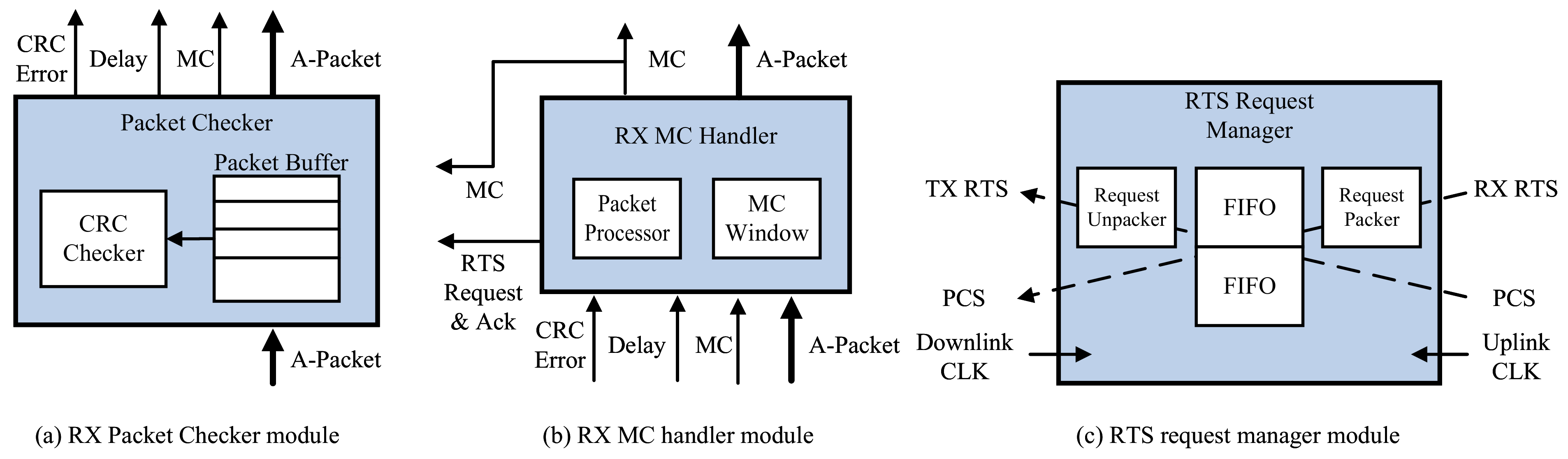
Figure 7, the structure of the RX RTS is composed of several modules: a Packet checker, an RX MC handler, an RX buffer, an RX scheduler, and an RTS request manager. The packet checker module is a module that checks the PHY field of the received A-Packet. The module extracts MC and Delay from the A-Packet header, transmits them, and checks whether CRC-8 and CRC-32 errors occur. At this time, the A-Packet is stored in the buffer to check the CRC-32 in the tail of the A-Packet.
Figure 11a shows the block diagram of the proposed packet inspector module. The RX MC handler module manages the received A-Packet with an MC window, similar to the TX MC handler. The RX MC handler decides whether to store, discard, or retransmit the A-Packet based on the status of the packet received from the packet checker.
Figure 11b shows the block diagram of the proposed RX MC handler.
When an A-Packet is received, first, CRC-8 errors are checked for. The received A-Packet is discarded if a header error is detected through CRC-8. Afterwards, the MC is used to check whether the A-Packet is missing. In addition, the CRC-32 value included in the A-Packet is compared with the CRC-32 value calculated by internal logic to check whether an error has occurred in the payload and then decide which retransmission request to perform. Finally, the transmission delay time of the A-PHY interface calculated through the Delay field is compared with the maximum retransmission delay time to determine whether to request retransmission. At this time, the maximum delay time that can occur due to one retransmission occurs when transmitting an A-Packet with the maximum length payload at the lowest standard PHY transmission rate, which is approximately 4 s.
Figure 12 shows the operation sequence according to packet status when receiving an A-Packet. A retransmission request is made by sending a retransmission request signal to the retransmission request manager along with A-Packet’s message counter (MC). Apart from the retransmission request, if there are no errors in the currently and previously received A-Packets, an acknowledgment signal is transmitted through the retransmission request manager.
The RX buffer in the RX RTS stores the received A-Packet and waits for the A-Packet request to be retransmitted. Like the TX buffer in the TX RTS, it consists of a controller and memory and stores and reads the A-Packet’s MC as the address. The memory size is also determined by the maximum size of the MC window, like the TX buffer. The RX scheduler transmits the A-Packet stored in the RX buffer to the data link layer according to the transmission order based on the MC. If a damaged A-Packet is stored in the RX buffer, the RX scheduler stops transmission and waits for the error to be restored through retransmission. If the error is not restored by the maximum retransmission delay time allowed in the A-PHY interface, the RX scheduler passes the damaged A-Packet as it is to the data link layer.
The retransmission request manager is a module that transmits the generated retransmission request and acknowledgment signal to the other side through downlink and uplink with different speeds. The retransmission request manager receives values from RX RTS and the PCS and transmits the retransmission request from RX RTS to the other side through the PCS. Therefore, the input from the PCS is the retransmission signal requested from the other side and delivered to TX RTS. At this time, because the operation speeds of the downlink and uplink are different, the retransmission request is transmitted using the FIFO module.
Figure 11c shows the block diagram of the proposed retransmission request manager.
4. Experimental Results
This section presents the verification environment of the A-PHY interface, including the proposed RTS layer. Moreover, the operation of the proposed RTS layer was verified in an FPGA, and the results of the ASIC design are shown.
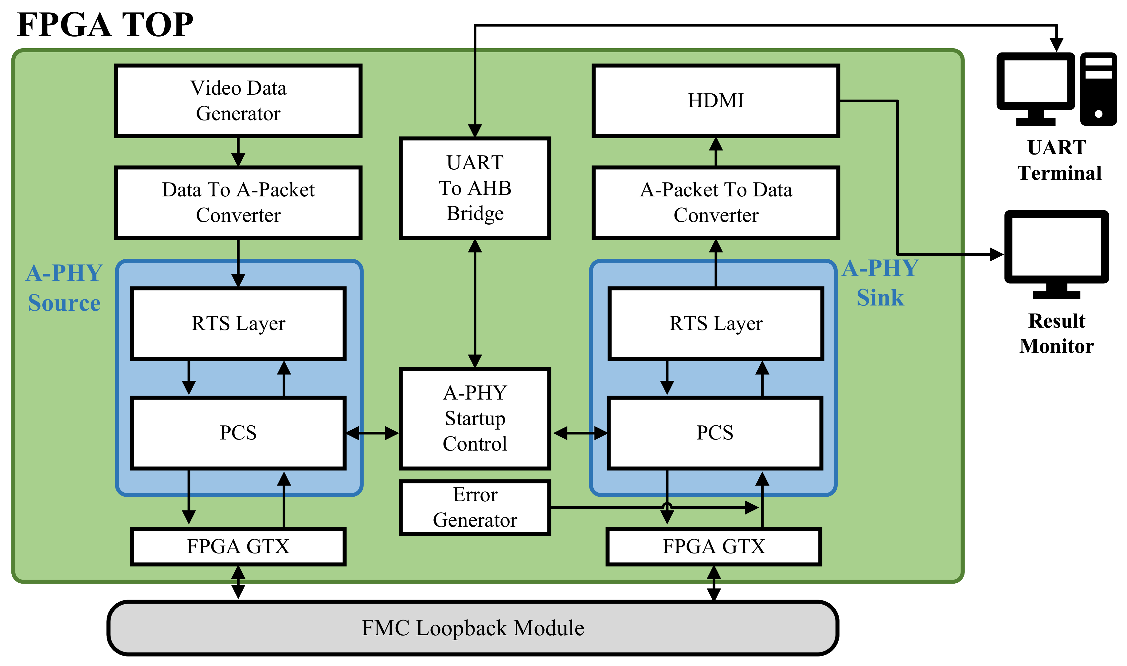
A block diagram for A-PHY verification, including the RTS layer, is shown in
Figure 13. It is composed of the A-PHY source, sink, and module for verification. The source and sink of the A-PHY interface consist of the RTS layer and an 8B10B PCS. The link layer of the A-PHY interface and higher protocol is implemented by replacing the video data generator that generates VGA (640 × 480)@60 fps videos, the HDMI interface that outputs video, and the converter module that converts data format. The transmission result of the A-PHY interface, including the RTS layer, is checked through the monitor connected via HDMI. The PMD that transmits actual data is implemented using a high-speed serial [
27] module of the FPGA, and the uplink and downlink are configured by connecting the FPGA mezzanine card loopback module. The downlink and uplink transmission rates are 2 Gbps and 100 Mbps. An UART to the AHB bridge module connects the A-PHY start-up control module and the host computer to control PCS start-up through the UART terminal. The error generator module was also inserted in front of the A-PHY sink to check the RTS specification.
For FPGA validation, we used a Xilinx KC705 development board [
28] and included the source and sink of the A-PHY interface and verification modules in one FPGA. The A-PHY environment, including serializer and deserializer (SerDes), was configured as shown in
Figure 14 using the FPGA GTX transceiver [
29], which is a high-speed serial interface for the KC705 board. In addition, an FPGA mezzanine card (FMC) loopback module [
30] from the company IAM was used. As shown in
Figure 14, the FMC loopback module reproduced the channel when transmitting and receiving data between the source and sink. The FMC loopback module allows easy prototyping, analysis, and testing of high-speed data links using the GTX transceiver provided by the FPGA board. At this time, the error generator module and RTS operation are controlled by a switch.
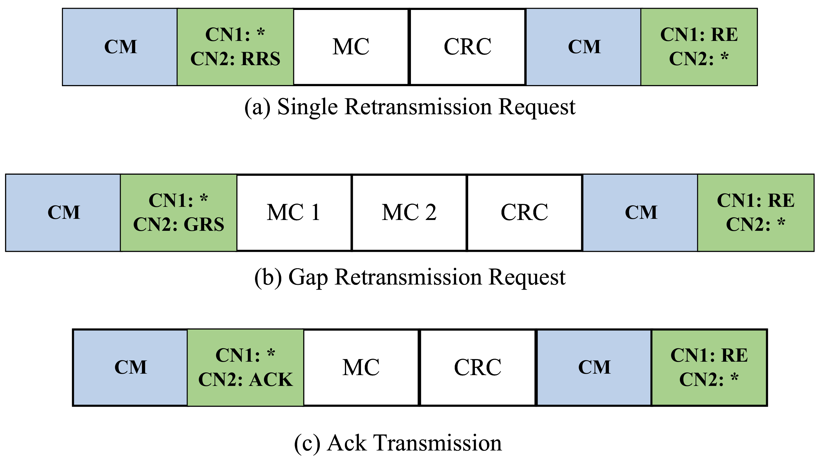
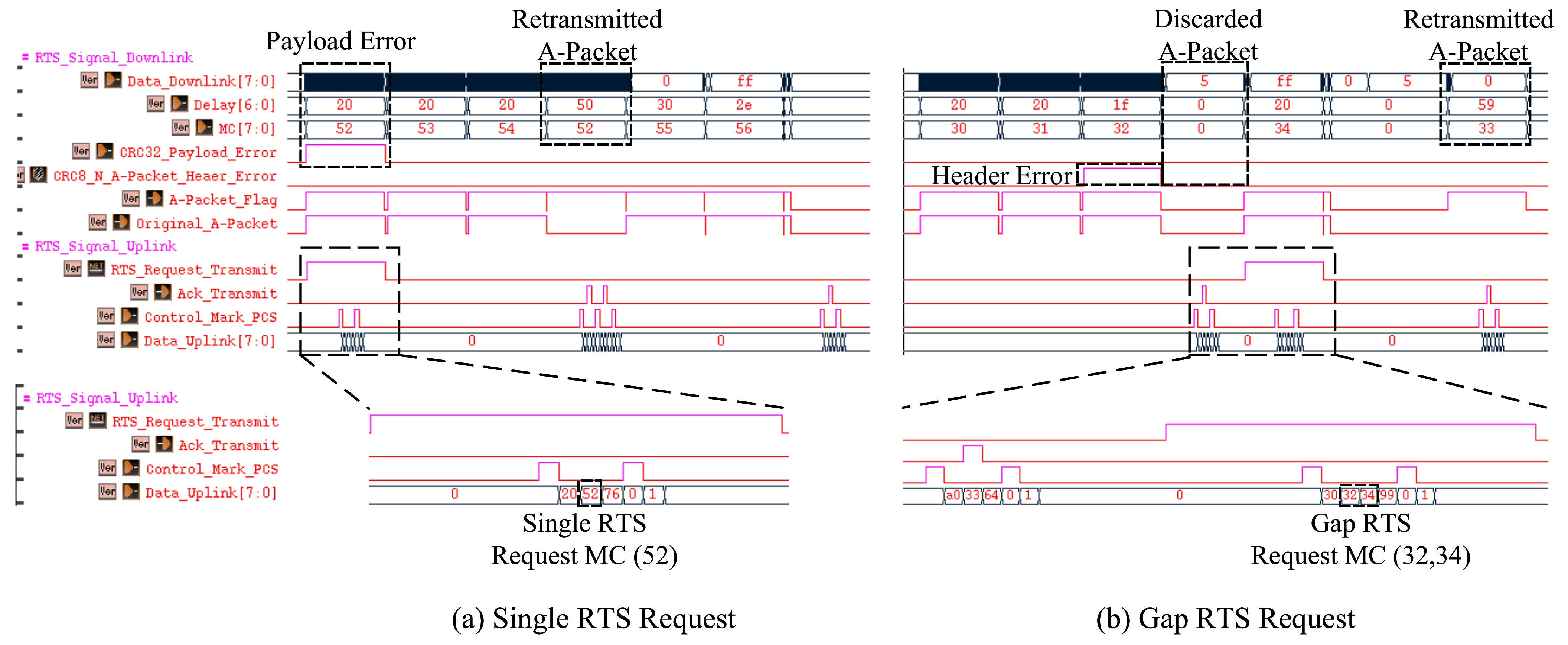
Figure 15 shows a waveform of the single and gap RTS requests.
Figure 15a is a simulation of a CRC32 error occurring in the received A-Packet where the error is corrected with a single RTS request. The RX RTS recognizes a problem in the payload of the A-Packet with an MC of 52 through the CRC32 error and transmits the single RTS request through the uplink. This single RTS request consists of the MC 52 of the A-Packet where the error occurred and the control data in the front and back. After that, it can be confirmed that the A-Packet in which the error occurred is retransmitted and received through the downlink.
Figure 15b is a simulation of error correction with gap RTS requests due to loss in the A-Packet. The A-Packet with MC 33 was discarded because a CRC8 error was detected in the header of the A-Packet. After that, the RX RTS receives the A-Packet of the MC 34, detects a loss, and sends the gap RTS request through the uplink. These gap RTS requests are similar to a single RTS request but transmit two message counters, 32 and 34, to indicate the range of loss. After that, it can be confirmed that the missed A-Packet is retransmitted and received through the downlink.
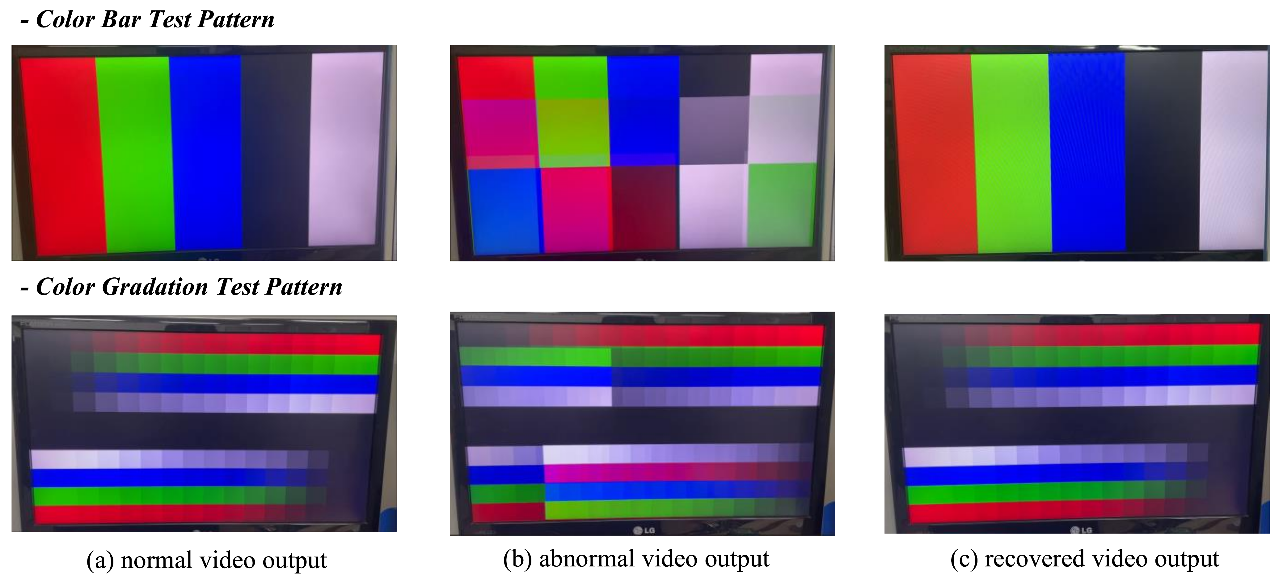
Figure 16 shows the video data transmitted through A-PHY being output through the monitor.
Figure 16a shows that the video created by the video data generator module is output to the monitor without the error insertion and RTS functions.
Figure 16b shows noise in the output video due to an error inserted with the error generation module in operation. Finally, when the RTS function is in operation, the error is corrected and a noise-free image is output, as shown in
Figure 16c.
Table 3 shows the FPGA synthesis results of the A-PHY source and sink, including the RTS layer. As a result of FPGA synthesis, 3924 LUTs and 2019 registers use less than 1% of resources and 132 block memories use approximately 30% of resources to store A-Packets in RTS operations. We confirmed that the proposed RTS hardware of the A-PHY interface does not use DSP. Moreover, the proposed system operates at up to 200 MHz on the KC705 FPGA board.
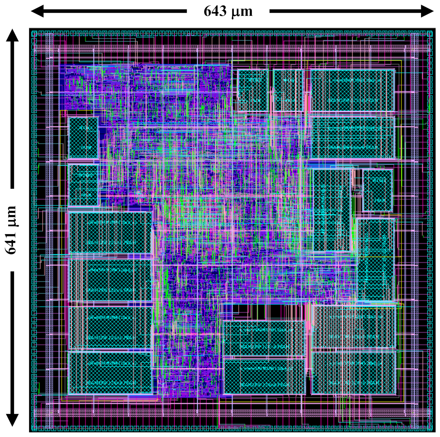
An ASIC was implemented in the SAED 28 nm process, an educational library provided by Synopsys [
31]. The TX/RX buffer that stores A-Packets in the RTS layer is a large-sized memory of approximately 50 KB, and therefore, it is not provided in the Synopsys’ Armenia Educational Department (SAED) 28 nm library, so it was excluded from the implementation. However, to connect the memory used in the TX/RX buffer from the outside, the pin was set as an in/out port, and place and route (P&R) was performed. The implementation used six metals, and only RVT CMOS devices were used. The layout, which is the result of ASIC implementation, is shown in
Figure 17. As shown in
Table 4, the memory used, excluding for the TX/RX buffer, is 1.36 KB, the number of logic gates is 25 K, and the chip area is 0.40 mm
. As a result of ASIC implementation in the A-PHY interface, the maximum operating frequency is 200 MHz.
5. Conclusions
In this paper, we proposed an architecture for the retransmission (RTS) layer, proposed an innovative physical layer, and further developed and validated the A-PHY interface, which encompasses the RTS Layer as an emerging vehicular Serializer/Deserializer (SerDes) standard. The proposed RTS hardware architecture integrates the RTS functionality by incorporating a CRC, a message counter (MC), and delay information into the PHY field of the A-Packet. Moreover, the proposed RTS architecture is aligned with the A-PHY interface standard. To validate the proposed A-PHY RTS architecture, an experimental environment utilizing an FPGA board was set up, through which the A-PHY RTS operation was confirmed. Additionally, the designed hardware was implemented as an ASIC. In future work, we plan to verify the MIPI A-PHY standard in a more realistic environment by connecting the source and sink with extremely long cables (up to 15 m) as defined in the A-PHY interface standard.


