
A Reliability-Enhanced Differential Sensing Amplifier for Hybrid CMOS/MTJ Logic Circuits


Abstract
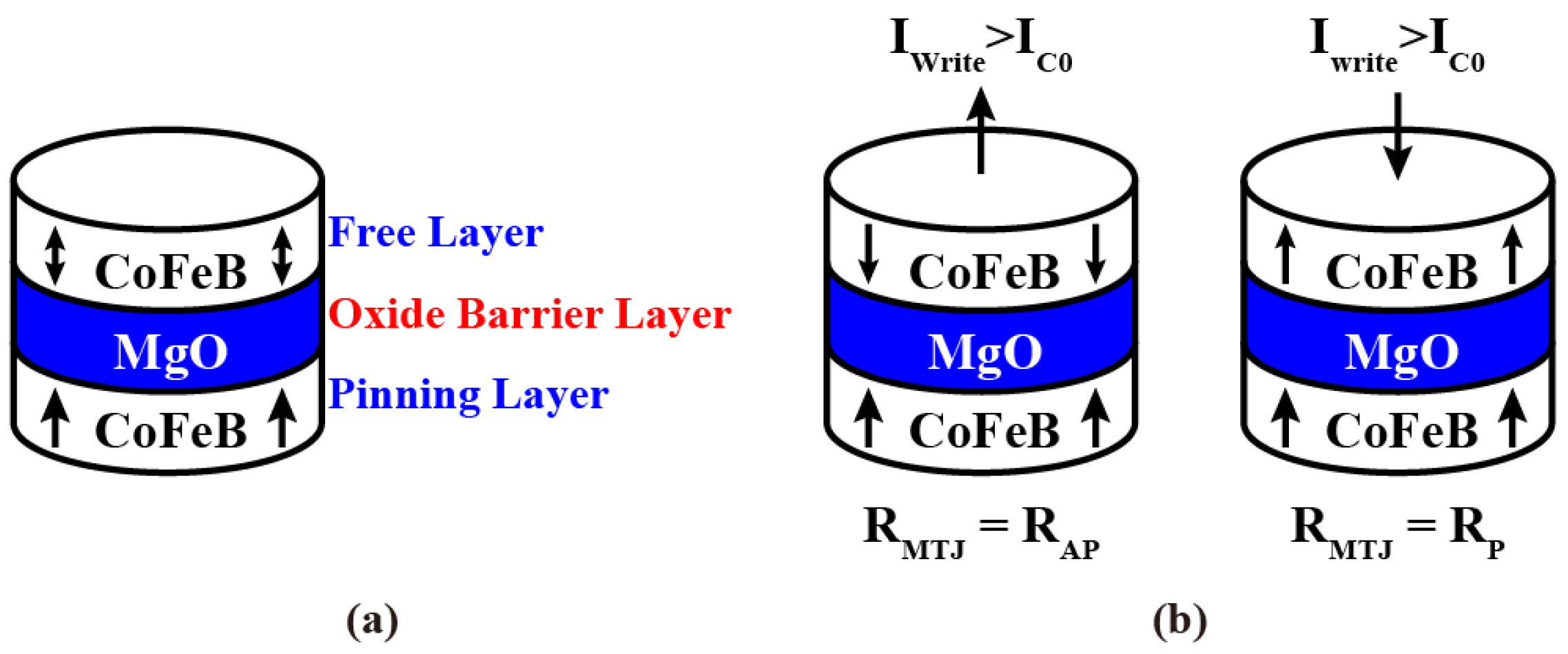
:1. Introduction
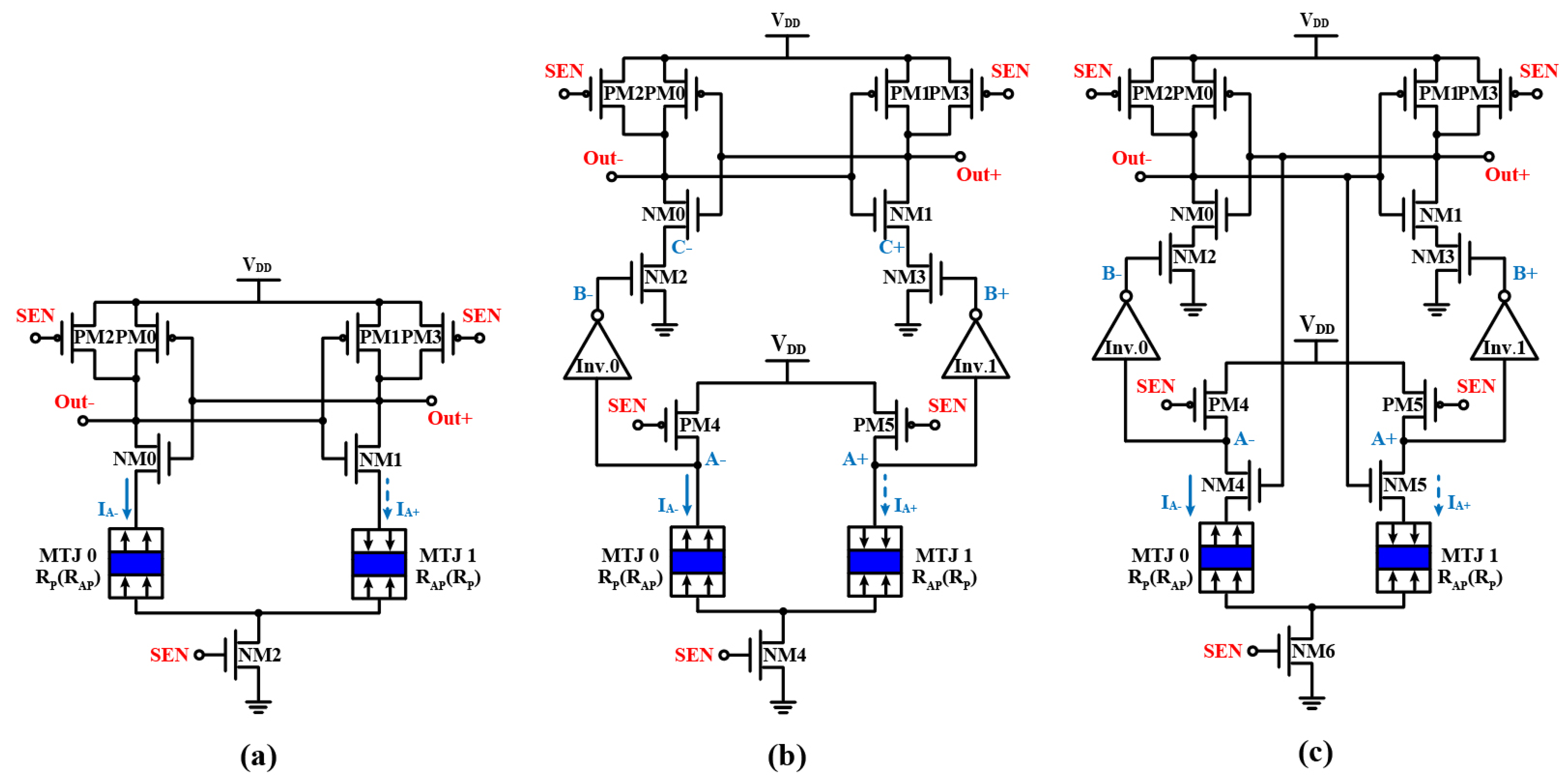
2. Proposed Reliability-Enhanced Differential Sensing Amplifier Circuit
3. Functional Verification
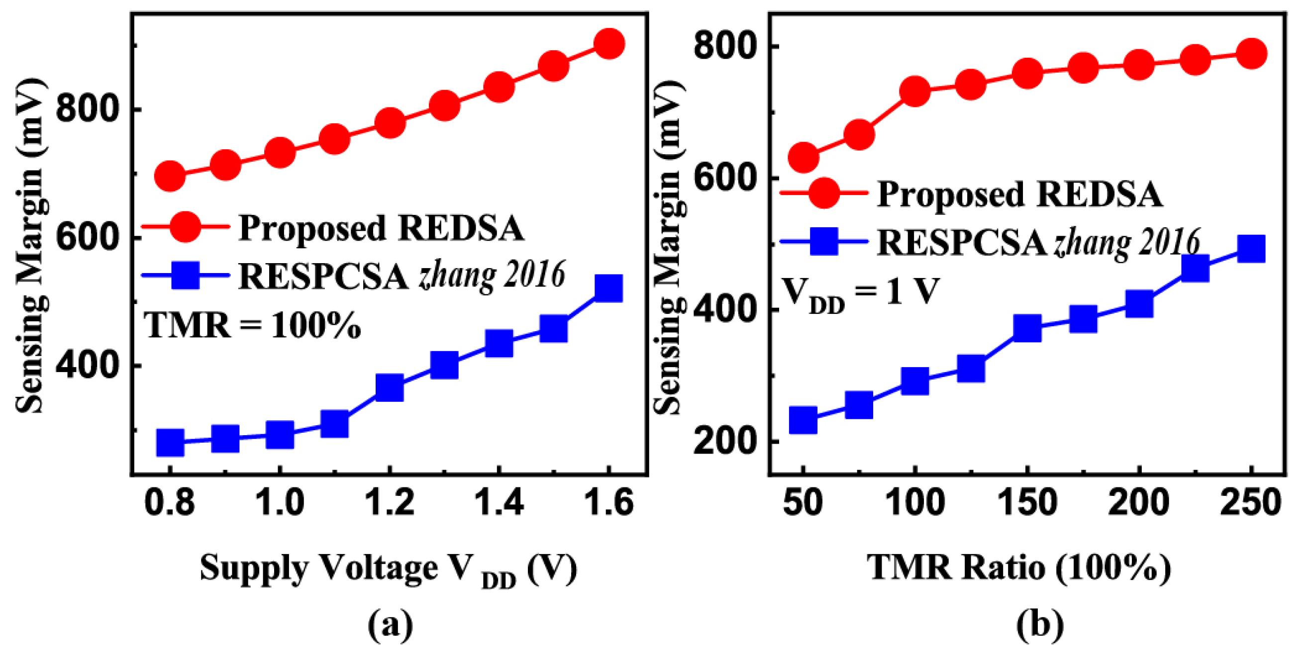
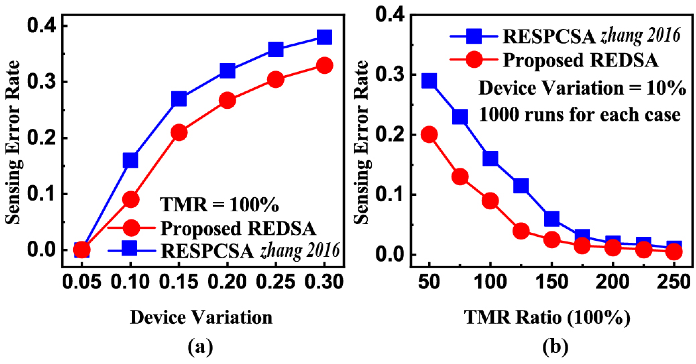
4. Performance Analysis and Comparison
4.1. Reliability Analysis and Comparative Discussion
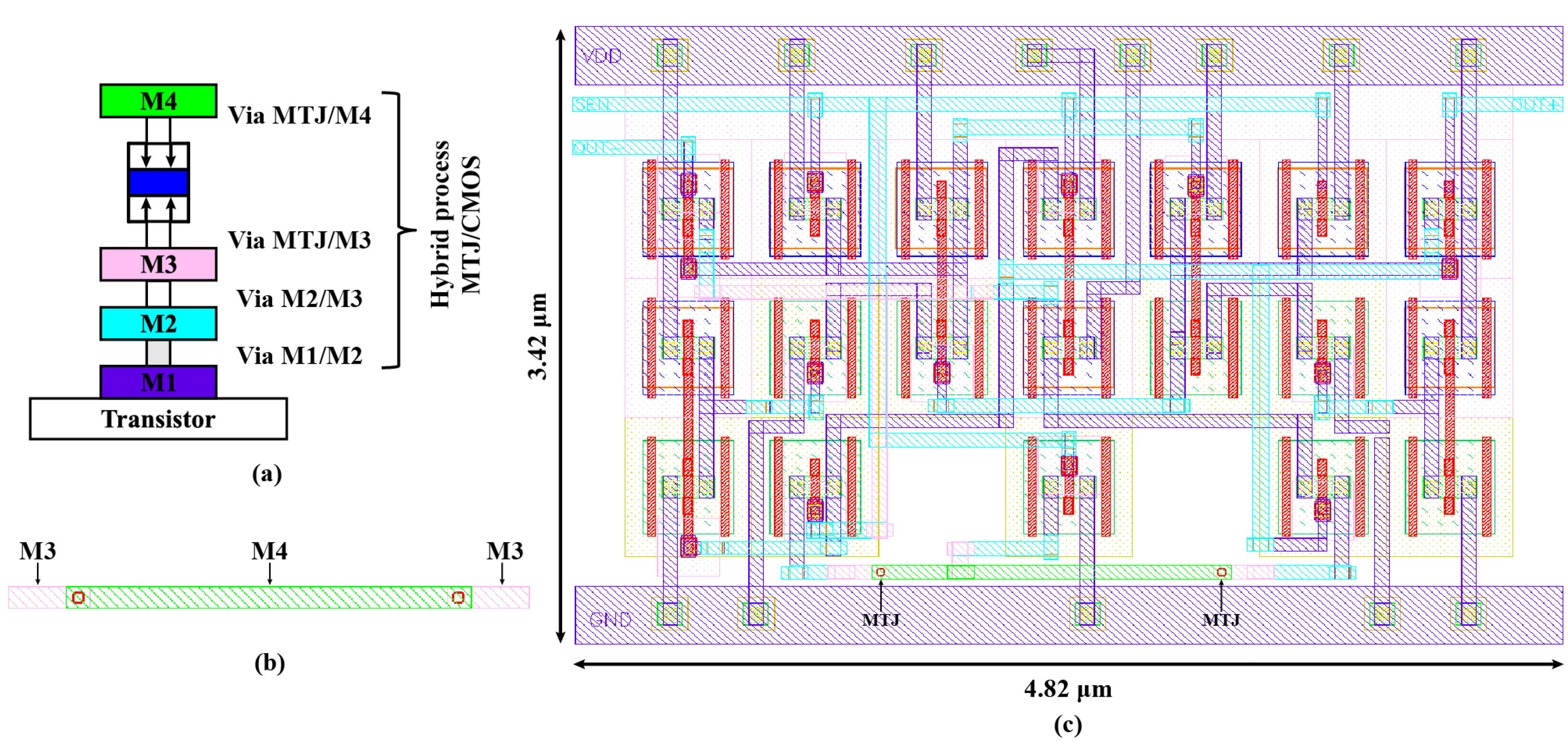
4.2. Layout of the Proposed REDSA
4.3. Performance Comparison
5. Conclusions
Author Contributions
Funding
Institutional Review Board Statement
Informed Consent Statement
Data Availability Statement
Conflicts of Interest
References
- Banerjee, W. Challenges and Applications of Emerging Nonvolatile Memory Devices. Electronics 2020, 9, 1029. [Google Scholar] [CrossRef]
- Swami, S.; Mohanram, K. Reliable Nonvolatile Memories: Techniques and Measures. IEEE Des. Test 2017, 34, 31–41. [Google Scholar] [CrossRef]
- Thapliyal, H.; Sharifi, F.; Kumar, S.D. Energy-Efficient Design of Hybrid MTJ/CMOS and MTJ/Nanoelectronics Circuits. IEEE Trans. Magn. 2018, 54, 1–8. [Google Scholar] [CrossRef]
- Chen, Y. ReRAM: History, status, and future. IEEE Trans. Electron Devices 2020, 67, 1420–1433. [Google Scholar] [CrossRef]
- Fantini, P. Phase change memory applications: The history, the present and the future. J. Phys. D Appl. Phys. 2020, 53, 283002. [Google Scholar] [CrossRef]
- Dieny, B.; Prejbeanu, I.L.; Garello, K.; Gambardella, P.; Freitas, P.; Lehndorff, R.; Raberg, W.; Ebels, U.; Demokritov, S.O.; Akerman, J.; et al. Opportunities and challenges for spintronics in the microelectronics industry. Nat. Electron. 2020, 3, 446–459. [Google Scholar] [CrossRef]
- Amirany, A.; Jafari, K.; Moaiyeri, M.H. High-Performance Spintronic Nonvolatile Ternary Flip-Flop and Universal Shift Register. IEEE Trans. Very Large Scale Integr. (VLSI) Syst. 2021, 29, 916–924. [Google Scholar] [CrossRef]
- Amirany, A.; Marvi, F.; Jafari, K.; Rajaei, R. Nonvolatile Spin-Based Radiation Hardened Retention Latch and Flip-Flop. IEEE Trans. Nanotechnol. 2019, 18, 1089–1096. [Google Scholar] [CrossRef]
- Natsui, M.; Yamagishi, G.; Hanyu, T. Design of a highly reliable nonvolatile flip-flop incorporating a common-mode write error detection capability. Jpn. J. Appl. Phys. 2021, 60, SBBB02. [Google Scholar] [CrossRef]
- Suzuki, D.; Hanyu, T. Design of a highly reliable, high-speed MTJ-based lookup table circuit using fractured logic-in-memory structure. Jpn. J. Appl. Phys. 2019, 58, SBBB10. [Google Scholar] [CrossRef]
- Jamshidi, V. NVRH-LUT: A nonvolatile radiation-hardened hybrid MTJ/CMOS-based look-up table for ultralow power and highly reliable FPGA designs. Turk. J. Electr. Eng. Comput. Sci. 2019, 27, 4486–4501. [Google Scholar] [CrossRef]
- Zhang, H.; Kang, W.; Wang, Z.; Deng, E.; Zhang, Y.; Zhao, W. High-density and fast-configuration non-volatile look-up table based on NAND-like spintronic memory. In Proceedings of the 2018 IEEE Asia Pacific Conference on Circuits and Systems (APCCAS), Chengdu, China, 26–30 October 2018; pp. 382–385. [Google Scholar] [CrossRef]
- Shukla, P.; Kumar, P.; Misra, P.K. A Highly Reliable, Dynamic Logic-Based Hybrid MTJ/CMOS Magnetic Full Adder for High-Performance and Low-Power Application. IEEE Trans. Magn. 2022, 58, 1–8. [Google Scholar] [CrossRef]
- Bae, G.Y.; Hwang, Y.; Lee, S.; Kim, T.; Park, W. Reconfigurable logic for carry-out computing in 1-bit full adder using a single magnetic tunnel junction. Solid-State Electron. 2019, 154, 16–19. [Google Scholar] [CrossRef]
- Deng, E.; Zhang, Y.; Kang, W.; Dieny, B.; Klein, J.-O.; Prenat, G.; Zhao, W. Synchronous 8-bit Non-Volatile Full-Adder based on Spin Transfer Torque Magnetic Tunnel Junction. IEEE Trans. Circuits Syst. I Regul. Pap. 2015, 62, 1757–1765. [Google Scholar] [CrossRef]
- Wang, C.; Zhang, D.; Zeng, L.; Zhao, W. Design of Magnetic Non-Volatile TCAM With Priority-Decision in Memory Technology for High Speed, Low Power, and High Reliability. IEEE Trans. Circuits Syst. I Regul. Pap. 2019, 67, 464–474. [Google Scholar] [CrossRef]
- Wang, C.; Zhang, D.; Zeng, L.; Deng, E.; Chen, J.; Zhao, W. A Novel MTJ-Based Non-Volatile Ternary Content-Addressable Memory for High-Speed, Low-Power, and High-Reliable Search Operation. IEEE Trans. Circuits Syst. I: Regul. Pap. 2018, 66, 1454–1464. [Google Scholar] [CrossRef]
- Arakawa, R.; Onizawa, N.; Diguet, J.-P.; Hanyu, T. Multi-Context TCAM-Based Selective Computing: Design Space Exploration for a Low-Power NN. IEEE Trans. Circuits Syst. I: Regul. Pap. 2020, 68, 67–76. [Google Scholar] [CrossRef]
- Natsui, M.; Suzuki, D.; Tamakoshi, A.; Watanabe, T.; Honjo, H.; Koike, H.; Nasuno, T.; Ma, Y.; Tanigawa, T.; Noguchi, Y.; et al. 12.1 An FPGA-Accelerated Fully Nonvolatile Microcontroller Unit for Sensor-Node Applications in 40nm CMOS/MTJ-Hybrid Technology Achieving 47.14 μW Operation at 200 MHz. In Proceedings of the 2019 IEEE International Solid-State Circuits Conference (ISSCC), San Francisco, CA, USA, 17–21 February 2019; pp. 202–204. [Google Scholar]
- Zheng, S.W.; Bi, J.S.; Xi, K.; Liu, J.; Liu, M.; Luo, L. A 28 nm full-margin, high-reliability, and ultra-low-power consumption sense amplifier for STT-MRAM. Microelectron. Reliab. 2019, 100–101, 113465. [Google Scholar] [CrossRef]
- Chen, J.; Yin, N.; Yu, Z. High speed, Low Resource and Non-volatile MTJ-CMOS Hybrid Logical Circuits. In Proceedings of the 2018 14th IEEE International Conference on Solid-State and Integrated Circuit Technology (ICSICT), Qingdao, China, 31 October–3 November 2018; pp. 1–3. [Google Scholar] [CrossRef]
- Kumar, S.D.; Thapliyal, H. Exploration of non-volatile MTJ/CMOS circuits for DPA-resistant embedded hardware. IEEE Trans. Magn. 2019, 55, 1–8. [Google Scholar] [CrossRef]
- Cai, H.; Han, M.; Wang, Y.; Naviner, L.; Liu, X.; Yang, J.; Zhao, W. Reliability emphasized MTJ/CMOS hybrid circuit towards ultra-low power. In Proceedings of the 2018 Conference on Design of Circuits and Integrated Systems (DCIS), Lyon, France, 14–16 November 2018; pp. 1–5. [Google Scholar] [CrossRef]
- Zhao, W.; Chappert, C.; Javerliac, V.; Noziere, J.-P. High Speed, High Stability and Low Power Sensing Amplifier for MTJ/CMOS Hybrid Logic Circuits. IEEE Trans. Magn. 2009, 45, 3784–3787. [Google Scholar] [CrossRef]
- Kang, W.; Deng, E.; Klein, J.-O.; Zhang, Y.; Zhang, Y.; Chappert, C.; Ravelosona, D.; Zhao, W. Separated Precharge Sensing Amplifier for Deep Submicrometer MTJ/CMOS Hybrid Logic Circuits. IEEE Trans. Magn. 2014, 50, 1–5. [Google Scholar] [CrossRef]
- Zhang, D.; Zeng, L.; Zhang, Y.; Klein, J.O.; Zhao, W. Reliability-Enhanced Hybrid CMOS/MTJ Logic Circuit Architecture. IEEE Trans. Magn. 2017, 53, 1–5. [Google Scholar] [CrossRef]
- Wang, Y.; Cai, H.; de Barros Naviner Naviner, L.A.; Zhang, Y.; Zhao, X.; Deng, E.; Klein, J.-O.; Zhao, W. Compact Model of Dielectric Breakdown in Spin-Transfer Torque Magnetic Tunnel Junction. IEEE Trans. Electron Devices 2016, 63, 1762–1767. [Google Scholar] [CrossRef]
- Zhang, Y.; Zhao, W.; Lakys, Y.; Klein, J.-O.; Kim, J.-V.; Ravelosona, D.; Chappert, C. Compact Modeling of Perpendicular-Anisotropy CoFeB/MgO Magnetic Tunnel Junctions. IEEE Trans. Electron Devices 2012, 59, 819–826. [Google Scholar] [CrossRef]
- Wang, Y.; Zhang, Y.; Deng, E.; Klein, J.; Naviner, L.; Zhao, W. Compact model of magnetic tunnel junction with stochastic spin transfer torque switching for reliability analyses. Microelectron. Reliab. 2014, 54, 1774–1778. [Google Scholar] [CrossRef]
- De Rose, R.; Lanuzza, M.; d’Aquino, M.; Carangelo, G.; Finocchio, G.; Crupi, F.; Carpentieri, M. A compact model with spin-polarization asymmetry for nanoscaled perpendicular MTJs. IEEE Trans. Electron Devices 2017, 64, 4346–4353. [Google Scholar] [CrossRef]
- Deng, E.; Kang, W.; Zhang, Y.; Klein, J.-O.; Chappert, C.; Zhao, W. Design Optimization and Analysis of Multicontext STT-MTJ/CMOS Logic Circuits. IEEE Trans. Nanotechnol. 2014, 14, 169–177. [Google Scholar] [CrossRef]
- Deng, E.; Anghel, L.; Prenat, G.; Zhao, W. Multi-context non-volatile content addressable memory using magnetic tunnel junctions. In Proceedings of the 2016 IEEE/ACM International Symposium on Nanoscale Architectures (NANOARCH), Beijing, China, 18–20 July 2016; pp. 103–108. [Google Scholar] [CrossRef]


| Parameter | Description | Default Value |
|---|---|---|
| tox | Oxide barrier thickness | 0.85 nm |
| tf | Free layer height | 1.3 nm |
| Area | MTJ surface | 402 × π/4 nm2 |
| V | Volume of free layer | Area × tf |
| R.A | Resistance × Area product | 5.0 Ω·μm2 |
| TMR(0) | the TMR ratio with zero Vbias | 100% |
| ΔTMR | the TMR ratio variation | 3% |
| Δtsl | Variation of free thickness | 3% |
| Δtox | Variation of oxide barrier thickness | 3% |
Disclaimer/Publisher’s Note: The statements, opinions and data contained in all publications are solely those of the individual author(s) and contributor(s) and not of MDPI and/or the editor(s). MDPI and/or the editor(s) disclaim responsibility for any injury to people or property resulting from any ideas, methods, instructions or products referred to in the content. |
© 2023 by the authors. Licensee MDPI, Basel, Switzerland. This article is an open access article distributed under the terms and conditions of the Creative Commons Attribution (CC BY) license (https://creativecommons.org/licenses/by/4.0/).
Share and Cite
Wang, C.; Yang, T.; Han, M.; Wang, D. A Reliability-Enhanced Differential Sensing Amplifier for Hybrid CMOS/MTJ Logic Circuits. Electronics 2023, 12, 447. https://doi.org/10.3390/electronics12020447
Wang C, Yang T, Han M, Wang D. A Reliability-Enhanced Differential Sensing Amplifier for Hybrid CMOS/MTJ Logic Circuits. Electronics. 2023; 12(2):447. https://doi.org/10.3390/electronics12020447
Chicago/Turabian StyleWang, Chengzhi, Tianqi Yang, Min Han, and Dongsheng Wang. 2023. "A Reliability-Enhanced Differential Sensing Amplifier for Hybrid CMOS/MTJ Logic Circuits" Electronics 12, no. 2: 447. https://doi.org/10.3390/electronics12020447
APA StyleWang, C., Yang, T., Han, M., & Wang, D. (2023). A Reliability-Enhanced Differential Sensing Amplifier for Hybrid CMOS/MTJ Logic Circuits. Electronics, 12(2), 447. https://doi.org/10.3390/electronics12020447