Communication

Ka-Band Three-Stack CMOS Power Amplifier with Split Layout of External Gate Capacitor for 5G Applications

School of Electric Engineering, Soongsil University, 369 Sangdo-ro, Dongjak-gu, Seoul 06978, Republic of Korea
*
Author to whom correspondence should be addressed.
Electronics 2023, 12(2), 432; https://doi.org/10.3390/electronics12020432
Submission received: 17 November 2022 / Revised: 8 January 2023 / Accepted: 12 January 2023 / Published: 13 January 2023
(This article belongs to the Special Issue RF/Microwave Circuits for 5G and Beyond)

Abstract

:
In this study, we designed a Ka-band two-stage differential power amplifier (PA) using a 65 nm RFCMOS process. To enhance the output power of the PA, a three-stack structure was utilized in the power stage, while the driver stage of the PA was designed with a common-source structure to minimize power consumption in the driver stage. The layout of an external gate capacitor for the stacked power stage was split to maximize the performance of the power transistor. With the proposed split layout of the external capacitor, gain, output power, and power-added efficiency (PAE) were improved. Additionally, a capacitive neutralization technique was applied to the power and driver stages to ensure the stability and enhance the gain of the PA. The measured P1dB and the saturation power were 22.0 dBm and 23.3 dBm, respectively, while the peak PAE was 27.8% at 28.5 GHz.

1. Introduction

With the rapid development of mobile communications, millimeter wave (mmWave) circuits to support mobile communications have been actively studied [1,2]. Especially, 5G wireless communication using beamforming technology is accelerating the development of array RF systems. In general, RF circuits based on compound semiconductors have a superior performance compared to CMOS-based RF circuits [3,4,5]. The relatively low breakdown voltage, nonlinearity, and high substrate loss of CMOS are the main causes of performance degradation of CMOS-based RF circuits. In particular, the low breakdown voltage is one of the major obstacles to obtaining high output power at the power amplifier (PA). In addition, high substrate loss causes the efficiency of the PA to decrease. On the other hand, the CMOS process has the advantage of a high integration level compared to the compound semiconductor process. Given that the array RF systems require a high integrity level, despite the several drawbacks of CMOS technology, research on mmWave circuits based on CMOS has been actively conducted [6].
In general, one of the most challenging mmWave circuits based on CMOS technology is considered to be PA [7,8,9,10]. Although the PA should generate high output power, the low breakdown voltage characteristics of CMOS make it difficult to obtain the high output power [11,12]. Accordingly, to achieve sufficient output power of the PA, various power combining techniques have been reported [13,14]. Among the various power combining techniques, a stacking technique, which can implement a voltage combining technique without using bulky transformers, has recently been vigorously studied in the Ka-band CMOS PA [15,16,17]. One of the key design methodologies of the stacking technique is the usage of an external gate capacitor to allow RF voltages at the gates of the stacked transistors and, consequently, equalize the voltage drop applied to each transistor [15,16,17]. As a result, the effects of the external gate capacitor should be even across the transistors. However, this is not easy to achieve due to the large size of the power transistors.
In this study, to maximize the effect of the external gate capacitance of the stacked PA, we propose a layout technique of the external gate capacitor. In order to ensure that the effect of the external gate capacitor can be distributed equally to the power transistor, the external gate capacitor was divided into two. The divided external gate capacitors were placed on both sides of the power transistor. It was confirmed that the efficiency and output power of the designed PA were improved thanks to the divided external gate capacitors. The power stage was designed with a three-stacked structure for sufficient output power, while a common-source structure was adopted in the driver stage to suppress dc power consumption. Additionally, to achieve the stability of the PA, a capacitive neutralization technique was also utilized.

2. Design of External Gate and Neutralization Capacitors

In this study, we designed a Ka-band CMOS PA. In particular, among the various frequency bands of 5G mobile communication, the target of this study was 27.5 GHz to 29.5 GHz. In the target frequency band, the P1dB and power-added efficiency (PAE) aimed to exceed 20.0 dBm and 20.0%, respectively.
Herein, we describe the design process of the Ka-band CMOS PA with a focus on the power stage. Throughout the design process, electromagnetic (EM) simulation was performed by default.

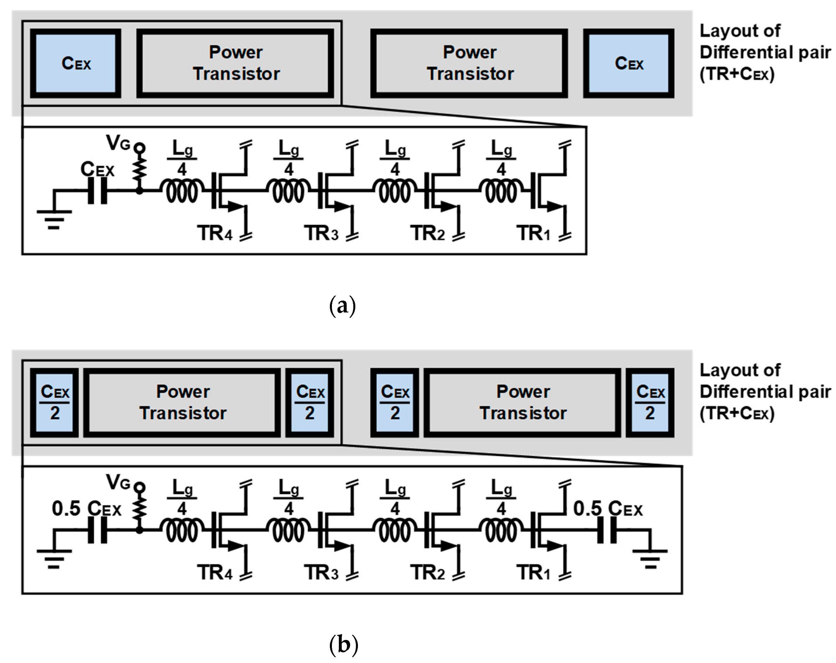
2.1. Determination of External Gate Capacitor Values

Figure 1 shows the designed schematic of the three stacked power stage. All six transistors used in the power stage have the same gate width of 480 μm, while having a gate length of 65 nm. As is well known from various previous studies, the optimum load impedance, ZLOAD, and acceptable supply voltage become higher as the number of stacked transistors increases. Therefore, when the number of stacked transistors increases, the output power of the power stage also increases. This operation of the stacked structure is affected by gate bias and the external gate capacitors of transistors constituting the stacked structure. In particular, gate bias and external gate capacitors directly affect the voltage drop in each transistor, and consequently affect the output power. To obtain the optimized value of external gate capacitors (CEX,2 and CEX,3), we utilized the following equations [15,17]:
Z d , k 1 = C g s , k + C E X , k + C g d , k 1 + g m , k Z d , k g m , k + s C g s , k C g d , k + C e x , k , Z d , k = k R O P T
C E X , k = C g s , k + C g d , k 1 + g m , k R O P T k 1 g m , k R O P T 1 , k = 2 , 3
where Cgs, Cgd, and gm are the gate-source parasitic capacitance, gate-drain parasitic capacitance, and trans-conductance of the transistors, respectively. Zd and ROPT are the load impedance of the transistors and optimum load resistance, respectively. In this study, MP,2 and MP,3 are identical to each other. Accordingly, under the conditions of the appropriate gate bias (VG,2 and VG,3), Cgs,2 and Cgs,3 are identical, and gm2 and gm3 are identical. With the extracted ROPT and gm2 (= gm3) of 10 Ω and 0.25 S, respectively, the ratio of CEX,2 and CEX,3 can be calculated as
C E X , 2 C E X , 3 = 2 g m R O P T 1 g m R O P T 1 2.3
With the result of Equation (3), the calculated and optimized values of CEX,2 and CEX,3 were 1.18 pF and 0.48 pF.
Figure 2 shows the simulated load-pull results with simple common-source, two-stacked, and three-stacked structures, with VDD of 1 V, 2 V, and 3 V, respectively. The real part of the optimum load impedance related to the output power increases as the number of stacked transistors increases. This means that the required impedance transformation ratio of the output matching network is reduced as the number of stacked transistors increases. In this work, a three- stacked structure was chosen considering the target output power of the PA.

2.2. Determination of Neutralization Capacitor Values

In this study, as shown in Figure 1, a capacitive neutralization technique was utilized to ensure stability in the high gain PA [18,19,20]. In Figure 3, the equivalent half-circuit of the common-source stage of Figure 1 is shown. CNEU is the capacitor for the capacitive neutralization technique. The value of CNEU is directly related to the value of Cgd and can be calculated as follows [21]:
C N E U = C g d 1 + r g / R S
where rg and RS are the parasitic gate resistance and the equivalent resistance connected to the gate of MP,1, respectively. The capacitive neutralization technique was used in the driver and power stages. Given that the transistors of the driver and power stages were 288 μm and 480 μm, respectively, the CNEU of power stage should be larger than that of driver stage.
To obtain the optimum values of CNEU for the power and driver stages, the maximum available gain (MAG) and k-factor according to the value of CNEU for the driver and power stages are shown in Figure 4. Here, the CNEU of the driver and power stages was defined as CNEU,D and CNEU,P, respectively. From the simulation results, we extracted the optimum values of CNEU for the driver and power stages as 80 fF and 120 fF, respectively. As can be seen in Figure 4, with the extracted optimum values of CNEU, the MAG and k-factor were simultaneously improved. Therefore, we designed the PA with the selected CNEU,D and CNEU,P at 80 fF and 120 fF, respectively. Under the selected CNEU,D and CNEU,P conditions, the driver and power stages were unconditionally stable, as shown in Figure 4. Figure 5 shows the stability circles of the driver and power stages in order to more clearly confirm that the driver and power stages are unconditionally stable with the selected CNEU,D and CNEU,P.

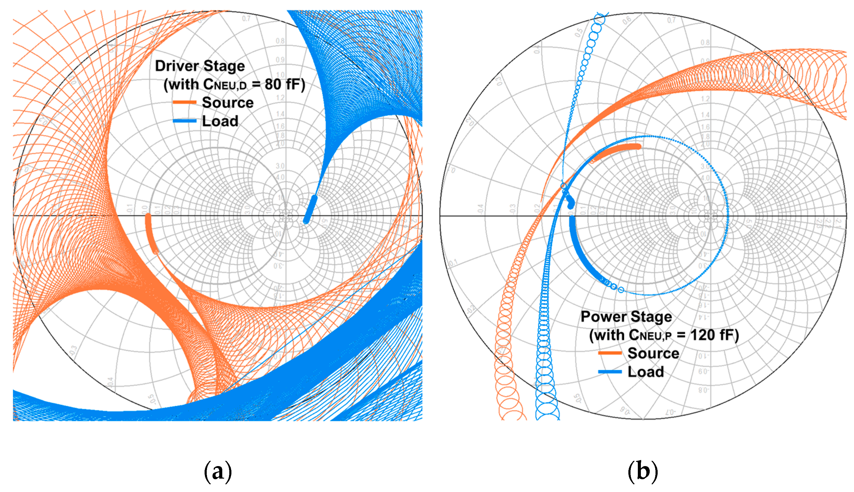
2.3. Design of Driver Stage

Figure 6 shows the schematic of the PA with the driver stage. The detail structure of the power stage of Figure 6 is shown in Figure 1. The output matching network of the power stage is completed with an output transformer and a capacitor, COUT.
Although the power stage is designed with the three-stack structure, the driver stage is designed with a differential common-source structure to reduce the dc power consumption with a relatively low supply voltage, resulting in the improving of the efficiency of overall PA. For the differential operation of the driver stage with a single-ended input signal, the transformer is used as a balun as well as a component of the input matching network. The transformer is also used for the inter-stage matching network, as shown in Figure 6.

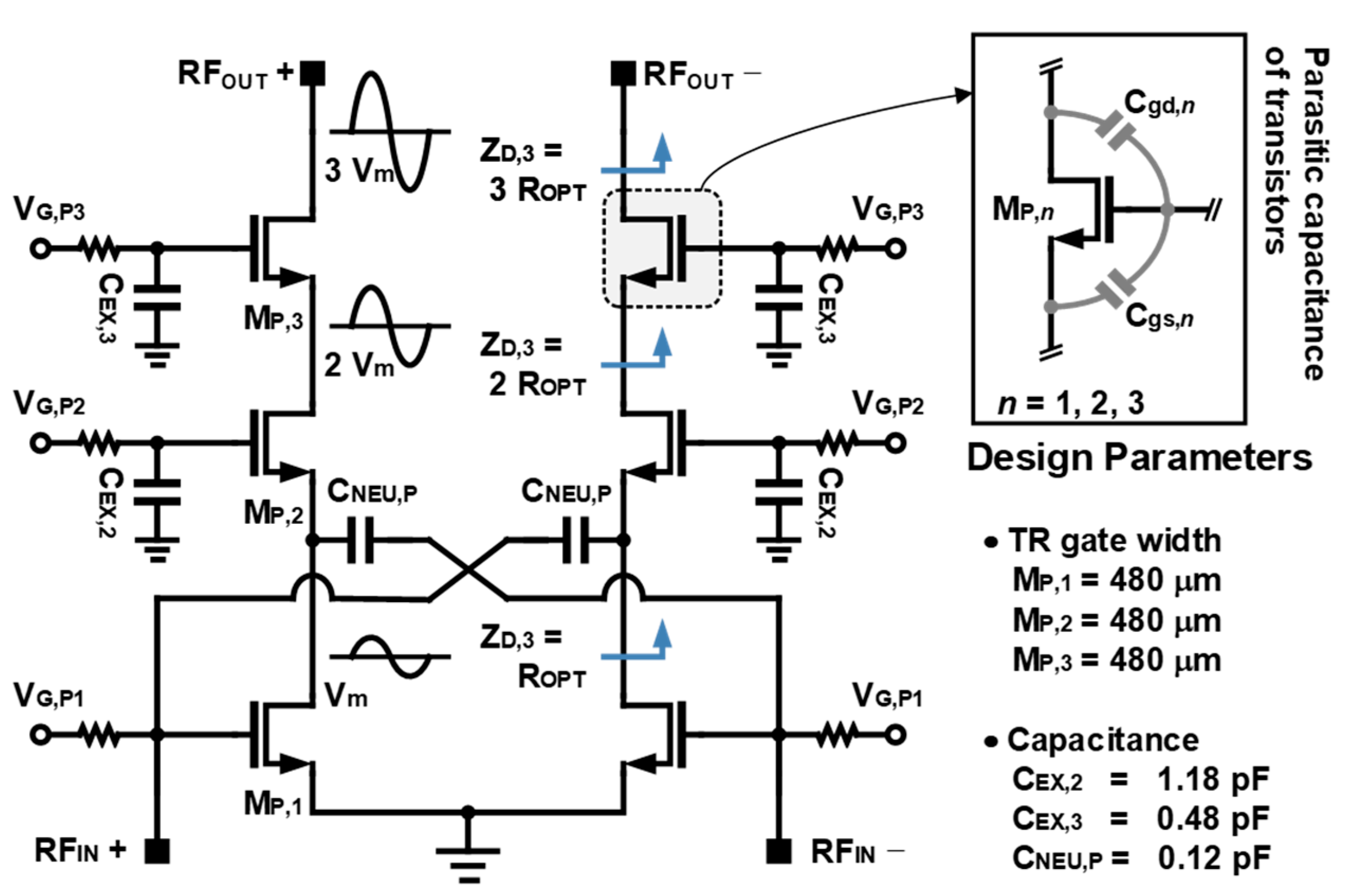
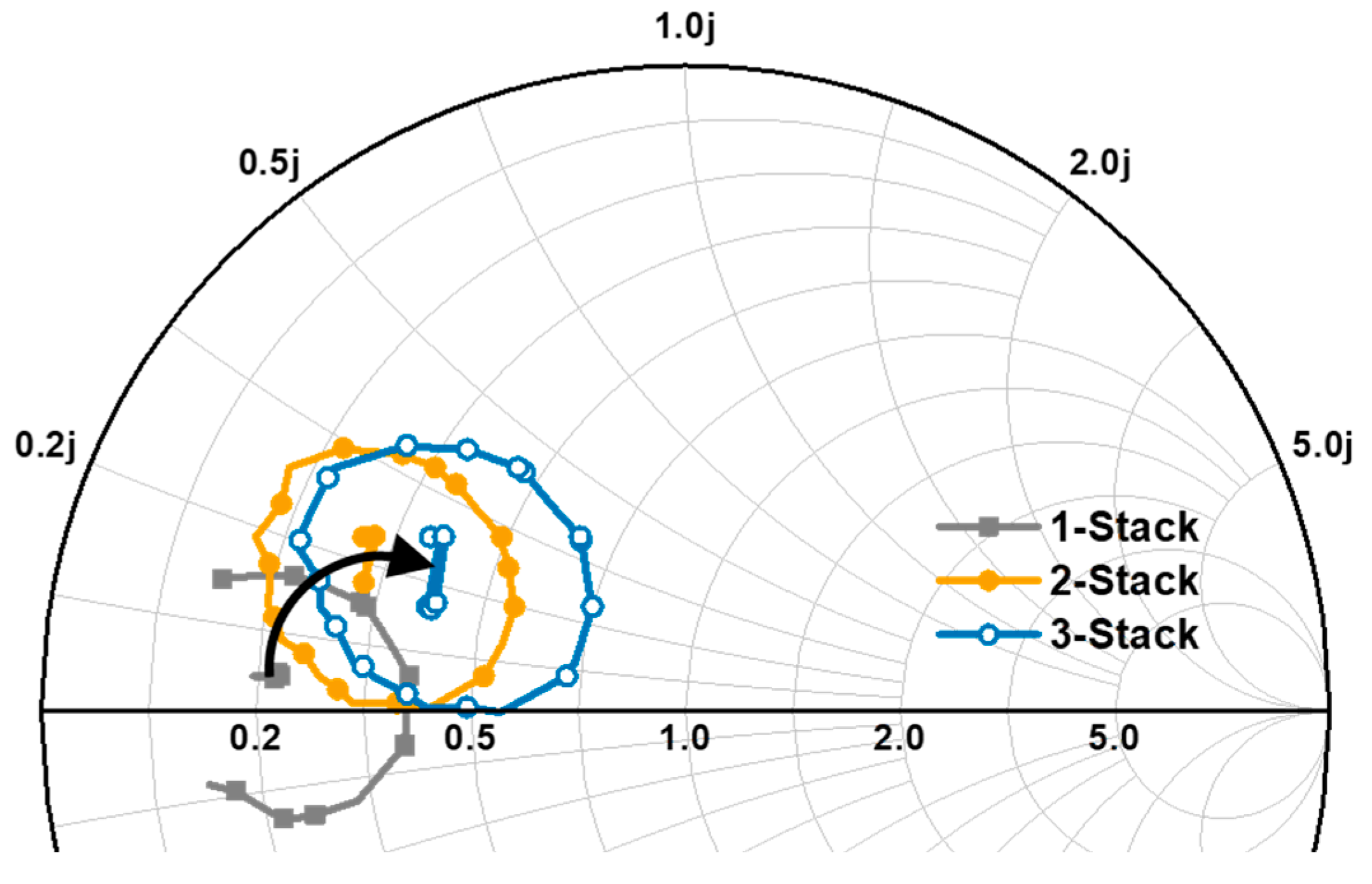
3. Design of Proposed Three-Stacked Power Amplifier with Split External Gate Capacitor

The proposed three-stacked PA with the split external gate capacitor was designed. In general, an external gate capacitor is located on the one side of the power transistor, as shown in Figure 7a. However, as shown in the simplified equivalent circuit of Figure 7a, because of the parasitic components of the metal lines for the power transistor, the effect of the external gate capacitor does not appear evenly through the power transistor. Here, the parasitic inductance induced by the metal lines of the power transistor is indicated as Lg. To overcome the problem of the typical layout, we proposed a layout technique of dividing the external gate capacitor into both sides of the power transistor, as shown in Figure 7b. The proposed technique allows the effect of the external gate capacitor to appear evenly through the power transistor, compared to the typical technique, so that the performance of the power transistor can be improved.
Although the gate metal of the power transistor is the distributed type in the actual situation, the equivalent circuit of the power transistor is simplified, as shown in Figure 8 for convenience of analysis. Figure 8a shows an equivalent circuit of a gate node of the power transistor in an ideal case without Lg. In this case, the gate node voltage Vg,eff,IDEAL of the transistor may be expressed as the follows.
V g , e f f , I D E A L = 1 1 / s C g s 1 / s C E X + 1 / s C g s V s
However, if Lg is considered, the Vg,eff,CON of Figure 8b is calculated as follows.
V g , e f f , C O N = 1 1 / s C g s 1 / s C E X + 1 / s C g s + s L g V s
Comparing Equation (6) considering Lg with Equation (5) in an ideal case, it can be seen that the gate node voltage is distorted by Lg. In particular, if the power transistor is formed in a distributed type as shown in Figure 7, the gate voltages of the unit-transistors constituting the power transistor are formed differently, causing the performance degradation of the PA. In order to minimize the effect of Lg, it is necessary to minimize Lg in Equation (6) to approach Equation (5).
In the case where the proposed layout technique is applied, the equivalent circuit is shown in Figure 9. In this case, Vg,eff,PRO may be expressed as follows.
V g , e f f , P R O = 1 1 / s C g s 1 / s C E X + 1 / s C g s + s L g / 4 V s
From Equations (6) and (7), compared to the typical technique, the proposed technique reduces the effect of Lg, bringing the voltage of the gate node of the power transistor closer to the ideal case. As a result, it may be seen that the proposed layout technique successfully alleviates the influence of Lg.
Figure 10 shows the actual layout of MP,2 and MP,3 applying the proposed layout technique of the external gate capacitor. In particular, when applying proposed technique, although the layout complexity slightly increases compared to the typical structure, no additional chip area is required to implement the proposed technique.
We compared the load-pull characteristics between the cases of applying the typical and the proposed layout techniques. As can be seen in Figure 11, the optimum impedances for the output power and efficiency of the proposed technique are almost similar to those of the typical one. However, the maximum output power and PAE of the proposed technique is higher than those of the typical technique.
The load-pull result was converted into the power gain and efficiency characteristics according to output power, as illustrated in Figure 12a. The power gain, P1dB, saturation power (Psat), and peak PAE with the proposed layout technique were improved compared to those with typical one. Even if the degree of improvement was not dramatic, all major performance indicators of the PA can be improved by simply dividing the external gate capacitor into two without an additional chip area. Figure 12b shows the simulation results of the S-parameters and k-factor. It can be seen that the S-parameters in the two cases were very similar to each other while the k-factor of the proposed technique was improved compared to the typical technique.

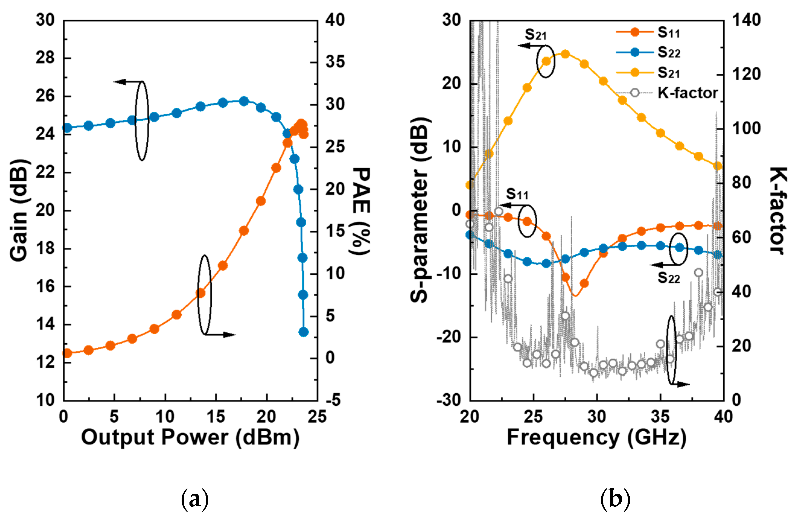
4. Results and Discussion

To verify the feasibility of the proposed layout technique of the external gate capacitor, we designed a Ka-band PA using 65 nm RFCMOS process which provides six metal layers. Figure 13 shows a photograph of the designed CMOS PA.
Figure 14a shows measured gain and PAE according to the output power at the operating frequency of 28.5 GHz. The measured P1dB and Psat were 22.0 dBm and 23.3 dBm, respectively, while the measured peak PAE was 27.8%. A gain expansion of approximately 1 dB occurred in the output power range from 6.75 dBm to 17.75 dBm, as shown in Figure 14a. Comparing the simulation results of PAE, the measurement result of the maximum PAE was approximately 4.2% lower. Figure 14b shows the measured S-parameters and k-factor. As can be seen in Figure 14b, the measured PA was unconditionally stable. In Figure 15, we summarized the measured P1dB, Psat, gain, and PAE according to the operating frequency. The maximum performance was obtained at the frequency of 28.5 GHz. In the design process, power matching technique using load-pull simulation was performed at the center frequency of 28.5 GHz, so the performance of P1dB and PAE was somewhat degraded as the operating frequency moved away from 28.5 GHz. In the frequency range of 27.5 GHz to 29.5 GHz, the flatness of the P1dB, Psat, gain, and PAE was lower than 1.2 dB, 0.8 dB, 2.8 dB, and 5.3%, respectively.
Figure 16 shows the error vector magnitude (EVM) and adjacent channel leakage ratio (ACLR) measured with 64-quadrature amplitude modulation (QAM), 100 MHz bandwidth, and 9.7 dB peak-to-average power ratio (PAPR) 5G new radio (NR) signal, respectively. In Figure 17, we summarized the measured maximum linear POUT and ACLR under the condition that the EVM value was −25 dB. Table 1 shows the performance of the Ka-band CMOS PAs available in the literature.

5. Conclusions

In this work, we proposed a split layout technique for the external gate capacitor of the stacked PA. In the typical and proposed structures, the effect of parasitic inductance that occurred in the gate node of the power transistor on the gate node voltage was analyzed. Through this, it was found that the proposed technique suppressed the influence of the parasitic inductance. By applying the proposed technique in the PA, the output power, gain, and PAE were simultaneously improved without the additionally required chip area. To verify the feasibility of the proposed technique, we designed a Ka-band three-stacked CMOS PA with a 65 nm RFCMOS process. The measured P1dB and Psat were 22.0 dBm and 23.3 dBm, respectively, while the maximum PAE was 27.8% at an operating frequency of 28.5 GHz. From the design and measurement results, it was successfully verified that the proposed technique could be easily applied to CMOS PA with a stacked structure.

Author Contributions

Conceptualization, J.Y. and C.P.; methodology, J.Y., J.L. and C.P.; investigation, J.Y.; supervision, C.P.; writing—original draft, J.Y., S.J. and H.J.; review and editing C.P. All authors have read and agreed to the published version of the manuscript.

Funding

This work was supported in part by the National Research Foundation of Korea (NRF) grant funded by the Korea government (MSIT) (No. 2021R1A2C1013666) and in part by the National Research Foundation of Korea (NRF) through the Korea Government (MSIT) under Grant NRF-2021R1A4A1032580.

Data Availability Statement

All the material conducted in the study is mentioned in article.

Conflicts of Interest

The authors declare no conflict of interest.

References

  1. Xiong, Y.; Zeng, X.; Li, J. A Frequency-Reconfigurable CMOS Active Phase Shifter for 5G mm-Wave Applications. IEEE Trans. Circuits Syst. II Express Briefs 2019, 67, 1824–1828. [Google Scholar] [CrossRef]
  2. Cho, G.; Hong, S. Ka-band CMOS Power Amplifier Based on Transmission Line Transformers with Single-Ended Doherty Network. IEEE Microw. Wirel. Components Lett. 2021, 31, 1. [Google Scholar] [CrossRef]
  3. Mayeda, J.C.; Lie, D.Y.C.; Lopez, J. A Highly Efficient 18–40 GHz Linear Power Amplifier in 40-nm GaN for mm-Wave 5G. IEEE Microw. Wirel. Components Lett. 2021, 31, 1008–1011. [Google Scholar] [CrossRef]
  4. Liu, R.-J.; Zhu, X.W.; Xia, J.; Zhao, Z.M.; Dong, Q.; Chen, P.; Zhang, L.; Jiang, X.; Yu, C.; Hong, W.; et al. A 24–28-GHz GaN MMIC Synchronous Doherty Power Amplifier with Enhanced Load Modulation for 5G mm-Wave Applications. IEEE Trans. Microw. Theory Tech. 2022, 70, 3910–3922. [Google Scholar] [CrossRef]
  5. Kim, T.; Im, H.; Lee, S.-H.; Kim, K.-J.; Park, C. Highly Linear K-/Ka-Band SPDT Switch Based on Traveling-Wave Concept in a 150-nm GaN pHEMT Process. IEEE Microw. Wireless Compon. Lett. 2022, 32, 987–990. [Google Scholar] [CrossRef]
  6. Qunaj, V.; Reynaert, P. A Ka-Band Doherty-Like LMBA for High-Speed Wireless Communication in 28-nm CMOS. IEEE J. Solid-state Circuits 2021, 56, 3694–3703. [Google Scholar] [CrossRef]
  7. Yu, C.; Feng, J.; Zhao, D. A 28-GHz Doherty Power Amplifier With a Compact Transformer-Based Quadrature Hybrid in 65-nm CMOS. IEEE Trans. Circuits Syst. II Express Briefs 2021, 68, 2790–2794. [Google Scholar] [CrossRef]
  8. Zong, Z.; Tang, X.; Khalaf, K.; Yan, D.; Mangraviti, G.; Nguyen, J.; Liu, Y.; Wambacq, P. A 28-GHz SOI-CMOS Doherty Power Amplifier With a Compact Transformer-Based Output Combiner. IEEE Trans. Microw. Theory Tech. 2021, 69, 2795–2808. [Google Scholar] [CrossRef]
  9. Park, J.; Kang, S.; Hong, S. Design of a Ka-Band Cascode Power Amplifier Linearized With Cold-FET Interstage Matching Network. IEEE Trans. Microw. Theory Tech. 2020, 69, 1429–1438. [Google Scholar] [CrossRef]
  10. Fan, T.-H.; Wang, Y.; Wang, H. A Broadband Transformer-Based Power Amplifier Achieving 24.5-dBm Output Power Over 24–41 GHz in 65-nm CMOS Process. IEEE Microw. Wirel. Components Lett. 2020, 31, 308–311. [Google Scholar] [CrossRef]
  11. Aoki, I.; Kee, S.; Rutledge, D.; Hajimiri, A. Distributed active transformer-a new power-combining and impedance-transformation technique. IEEE Trans. Microw. Theory Tech. 2002, 50, 316–331. [Google Scholar] [CrossRef] [Green Version]
  12. Park, C.; Kim, Y.; Kim, H.; Hong, S. A 1.9-GHz CMOS Power Amplifier Using Three-Port Asymmetric Transmission Line Transformer for a Polar Transmitter. IEEE Trans. Microw. Theory Tech. 2007, 55, 230–238. [Google Scholar] [CrossRef] [Green Version]
  13. Wang, J.; Zhu, W.; Wang, R.; Wang, Y. A Dual-Mode W-Band Eight-Way Parallel–Series Power-Combining PA with +18-dBm Psat and 15.1% PAE in 65-nm CMOS Technology. IEEE Microw. Wireless Compon. Lett. 2022, 32, 149–152. [Google Scholar] [CrossRef]
  14. Zhang, L.; Ma, K.; Fu, H. A 60-GHz 32-Way Hybrid Power Combination Power Amplifier in 55-nm Bulk CMOS. IEEE Trans. Microw. Theory Tech. 2022, 2022, 1–15. [Google Scholar] [CrossRef]
  15. Dabag, H.-T.; Hanafi, B.; Golcuk, F.; Agah, A.; Buckwalter, J.F.; Asbeck, P.M. Analysis and Design of Stacked-FET Millimeter-Wave Power Amplifiers. IEEE Trans. Microw. Theory Tech. 2013, 61, 1543–1556. [Google Scholar] [CrossRef]
  16. Wu, C.-W.; Lin, Y.-H.; Hsiao, Y.-H.; Chou, C.-F.; Wu, Y.-C.; Wang, H. Design of a 60-GHz High-Output Power Stacked- FET Power Amplifier Using Transformer-Based Voltage-Type Power Combining in 65-nm CMOS. IEEE Trans. Microw. Theory Tech. 2018, 66, 4595–4607. [Google Scholar] [CrossRef]
  17. Jeong, H.; Lee, H.D.; Park, B.; Jang, S.; Kong, S.; Park, C. Three-Stacked CMOS Power Amplifier to Increase Output Power With Stability Enhancement for mm-Wave Beamforming Systems. IEEE Trans. Microw. Theory Tech. 2022, 2022, 1–15. [Google Scholar] [CrossRef]
  18. Chen, Y.-C.; Lin, Y.-H.; Lin, J.-L.; Wang, H. A Ka-Band Transformer-Based Doherty Power Amplifier for Multi-Gb/s Application in 90-nm CMOS. IEEE Microw. Wirel. Components Lett. 2018, 28, 1134–1136. [Google Scholar] [CrossRef]
  19. Fang, X.; Xia, J.; Boumaiza, S. A 28-GHz Beamforming Doherty Power Amplifier With Enhanced AM-PM Characteristic. IEEE Trans. Microw. Theory Tech. 2020, 68, 3017–3027. [Google Scholar] [CrossRef]
  20. Jeong, H.; Lee, H.; Park, B.; Jang, S.; Kong, S.; Park, C. Optimization Technique for High-Gain CMOS Power Amplifier for 5G Applications. Appl. Sci. 2021, 11, 11691. [Google Scholar] [CrossRef]
  21. Chan, W.L.; Long, J.R. A 58–65 GHz Neutralized CMOS Power Amplifier With PAE Above 10% at 1-V Supply. IEEE J. Solid-state Circuits 2010, 45, 554–564. [Google Scholar] [CrossRef]
  22. Huang, W.-C.; Wang, H. An inductive-neutralized 26-dBm K-/Ka-band power amplifier with 34% PAE in 90-nm CMOS. IEEE Trans. Microw. Theory Tech. 2019, 67, 4427–4440. [Google Scholar] [CrossRef]
  23. Lee, J.; Hong, S. A 24–30 GHz 31.7% Fractional Bandwidth Power Amplifier With an Adaptive Capacitance Linearizer. IEEE Trans. Circuits Syst. II Express Briefs 2020, 68, 1163–1167. [Google Scholar] [CrossRef]
  24. Lee, S.; Kang, S.; Hong, S. A 28-GHz CMOS Linear Power Amplifier With Low Output Phase Variation Over Dual Power Modes. IEEE Microw. Wirel. Components Lett. 2019, 29, 551–553. [Google Scholar] [CrossRef]
Figure 1. Schematic of the three stacked power stage with differential structure.
Electronics 12 00432 g001
Figure 2. Load-pull simulation results of stacked power stage.
Electronics 12 00432 g002
Figure 3. Equivalent half-circuit of the differential common-source structure with the neutralization capacitor.
Electronics 12 00432 g003
Figure 4. Simulated MAG and K-factor according to the neutralization capacitor: (a) driver and (b) power stages.
Electronics 12 00432 g004
Figure 5. Simulated stability circles with selected neutralization capacitors: (a) driver and (b) power stages.
Electronics 12 00432 g005
Figure 6. Schematic of the designed PA.
Electronics 12 00432 g006
Figure 7. Conceptual layout of the differential power transistor with neutralization capacitor: (a) typical and (b) proposed layout techniques.
Electronics 12 00432 g007
Figure 8. Equivalent circuits of power transistor with typical layout technique: (a) ideal case and (b) case considering parasitic inductance, Lg.
Electronics 12 00432 g008
Figure 9. Equivalent circuits of power transistor with proposed layout technique.
Electronics 12 00432 g009
Figure 10. Layout of the power transistor with proposed split external gate capacitor.
Electronics 12 00432 g010
Figure 11. Load-pull simulation results of stacked power stage with (a) typical and (b) proposed layout techniques.
Electronics 12 00432 g011
Figure 12. Simulation results: (a) gain and PAE and (b) S-parameters.
Electronics 12 00432 g012
Figure 13. Chip photograph of the designed PA (core size: 0.725 × 0.500 mm2).
Electronics 12 00432 g013
Figure 14. Measurement results: (a) gain and PAE and (b) S-parameters.
Electronics 12 00432 g014
Figure 15. Measurement results: P1dB, Psat, gain, and PAE according to the frequency.
Electronics 12 00432 g015
Figure 16. Measurement results with modulation signal (64-QAM, 100 MHz bandwidth, 9.7 dB PAPR): (a) EVM and (b) ACLR.
Electronics 12 00432 g016
Figure 17. Measurement results: PMAX and ACLR according to the frequency with modulation signal (64-QAM, 100 MHz bandwidth, 9.7 dB PAPR).
Electronics 12 00432 g017
Table 1. Comparison with state-of-the-art of CMOS PAs.
TMTT ’19
[22]
TCAS-II ’21
[23]
MWCL ’19
[24]
Proposed Work
Tech. (nm)90286565
Freq. (GHz)28.030.028.028.5
P1dB (dBm)23.217.216.522.0
Gain (dB)16.321.218.023.3
Peak PAE (%)34.130.327.327.7
Modulation
/Bandwidth
64-QAM
/100 MHz
64-QAM
/100 MHz
64-QAM
/100 MHz
64-QAM
/100 MHz
EVM (dBc)−25.0−25.0−25.0−25.0
POUT @EVM (dBm)19.010.97.517.3
Core size (mm2)0.4010.820.4560.36
Topology1-stage
Cascode
2-stage
Cascode
2-stage
Cascode
2-stage
3-stack
Disclaimer/Publisher’s Note: The statements, opinions and data contained in all publications are solely those of the individual author(s) and contributor(s) and not of MDPI and/or the editor(s). MDPI and/or the editor(s) disclaim responsibility for any injury to people or property resulting from any ideas, methods, instructions or products referred to in the content.

