Article

A CMA-Based Electronically Reconfigurable Dual-Mode and Dual-Band Antenna

by
Nicholas E. Russo
,
Constantinos L. Zekios
* and
Stavros V. Georgakopoulos
College of Engineering and Computing, Florida International University (FIU), Miami, FL 33174, USA
*
Author to whom correspondence should be addressed.
Electronics 2023, 12(18), 3915; https://doi.org/10.3390/electronics12183915
Submission received: 19 August 2023 / Revised: 13 September 2023 / Accepted: 15 September 2023 / Published: 17 September 2023
(This article belongs to the Special Issue Recent Advances in Antenna Arrays and Millimeter-Wave Components)

Abstract

:
In this work, an electronically reconfigurable dual-band dual-mode microstrip ring antenna with high isolation is proposed. Using characteristic mode analysis (CMA), the physical characteristics of the ring antenna are revealed, and two modes are appropriately chosen for operation in two sub-6 GHz “legacy” bands. Due to the inherent orthogonality of the characteristic modes, measured isolation larger than 37 dB was achieved in both bands without requiring complicated decoupling approaches. An integrated electronically reconfigurable matching network (comprising PIN diodes and varactors) was designed to switch between the two modes of operation. The simulated and measured results were in excellent agreement, showing a peak gain of 4.7 dB for both modes and radiation efficiency values of 44.3 % and 64 % , respectively. Using CMA to gain physical insights into the radiative orthogonal modes of under-researched and non-conventional antennas (e.g., antennas of arbitrary shapes) opens the door to developing highly compact radiators, which enable next-generation communication systems.

1. Introduction

The terminals of modern communication systems use multiple antennas to cover selected bands in the 0.8–80 GHz range. For example, today’s cellular phones must support 8 × 8 MIMO in the sub-6 GHz band and contain two or more phased arrays for beamforming in mmWave bands [1]. Also, such antennas must fit into electrically small volumes and conform to the internal structures of communication terminals. These requirements have motivated innovative antenna designs and methods to mitigate coupling, especially in the cellular phone industry [2]. Conventionally, antenna designers begin by using standard configurations (e.g., PIFAs or planar monopoles) with significant non-diagonal elements in their impedance matrix, i.e., significant mutual coupling. Then, antenna designers must attempt to find the appropriate transformation that can diagonalize their impedance matrix.
In theory, the most straightforward and general decoupling method is to connect the antennas to a network that applies the matrix diagonalization transformation, i.e., a decoupling network. However, in practice, decoupling networks are lossy and increasingly complex as the number of antennas increases [3]. These problems have motivated the development of “custom” decoupling methods for specific types of antenna designs. Therefore, such methods have limited applicability but are generally simpler to design. Typically, custom decoupling methods introduce additional structures, such as periodic structures, coupling-mode transducers, defected-ground structures, and wave traps. For example, periodic structures such as electromagnetic band gap (EBG) and artificial magnetic conductors (AMCs) have been used to suppress surface waves between microstrip patch antennas [4] and provide electrically compact and low-profile designs [5] with isolation larger than 10 dB. However, periodic structures significantly increase the size and fabrication complexity of antennas, especially at frequencies over 30 GHz. Alternatively, coupling-mode transducers have been used to achieve isolation larger than 20 dB with minimal increase in antenna volume. However, such transducers are typically challenging to design and cannot be used for dual-polarized designs [6]. A more straightforward decoupling method relies on perturbations of the ground plane at the expense of increased back-lobe radiation [7]. Also, another simple decoupling method is to use several wave traps or vias among the antenna elements to provide additional coupling paths that cancel the coupling among the antenna elements; however, this method increases the losses of designs [8].
Multiple modes can be excited on either (a) separate, isolated apertures that are in close electrical proximity or (b) the same aperture to maximize compactness. In [9], dipoles separated by 0.019 λ o were excited in the differential and common modes, respectively, resulting in 24.2 dB isolation. Also, in [10], the electric and magnetic symmetry in substrate-integrated waveguide cavities was used to separate the cavity into quarters with isolation better than 22 dB. In [11], a wide-band antenna was achieved by having monopole and dipole modes share the aperture in the lower band, while slot and open-slot modes shared the aperture in the upper band, with isolation better than 21 dB. Similarly, in [12], slot and loop modes were excited on the same aperture, with isolation better than 19 dB.
Although these shared-aperture, multimode antenna designs are compact, they rely on the utilization of well-known modes, e.g., slot, dipole, monopole, and loop. Practical designs, e.g., designs with low profiles, which only use well-known modes to integrate many antennas, are generally complex and struggle to achieve isolation better than 10 dB, e.g., [13]. This motivates the design of non-conventional planar antenna structures, which can approach the fundamental limits on the number of antennas that can be packed into a given volume [14,15,16]. A popular method to analyze non-conventional structures is characteristic mode analysis (CMA). CMA was first introduced by Garbacz in [17] and was later refined in [18,19]. Recently, due to the physical intuition it provides [20], CMA has grown in popularity and has driven innovation in, e.g., low-profile wide-band antennas [21,22]; multiport antennas [23]; multiband, wide-band, and MIMO antennas [24]; isolation enhancement techniques [25]; radiation pattern optimization and synthesis techniques [26]. For a full review of the applications of CMA to radiating, scattering, and coupling problems, the interested reader is referred to [27,28].
In this work, CMA is applied to a square microstrip ring antenna. The microstrip ring is popular as a miniaturized replacement of the conventional rectangular patch antenna that provides improved bandwidth and directivity. Therefore, most works study the T M 10 or T M 01 mode for broadside radiation [29,30,31], although higher-order modes, such as T M 11 and T M 12 , have been studied for multiband operation [32]. In this work, CMA is used to identify two non-conventional higher-order modes on the ring antenna that provide complementary radiation patterns. Following the approach of mode/pattern reconfigurable antennas [33,34], an electronically reconfigurable feed network is designed to excite the two modes. Notably, the complementary radiation patterns of the two modes (here referred to as modes 1 and 2) act as sum and difference beams. This makes the proposed antenna a good candidate for low-monopulse radar tracking, which is a more cost-effective solution than traditionally expensive phased arrays [35].
This paper is organized as follows: Section 2 briefly reviews CMA and applies it to identify orthogonal modes on the microstrip ring antenna. Section 3 develops ideal and practical methods to excite two of the identified modes. Section 4 compares simulated and measured results. Finally, conclusions are drawn in Section 5.

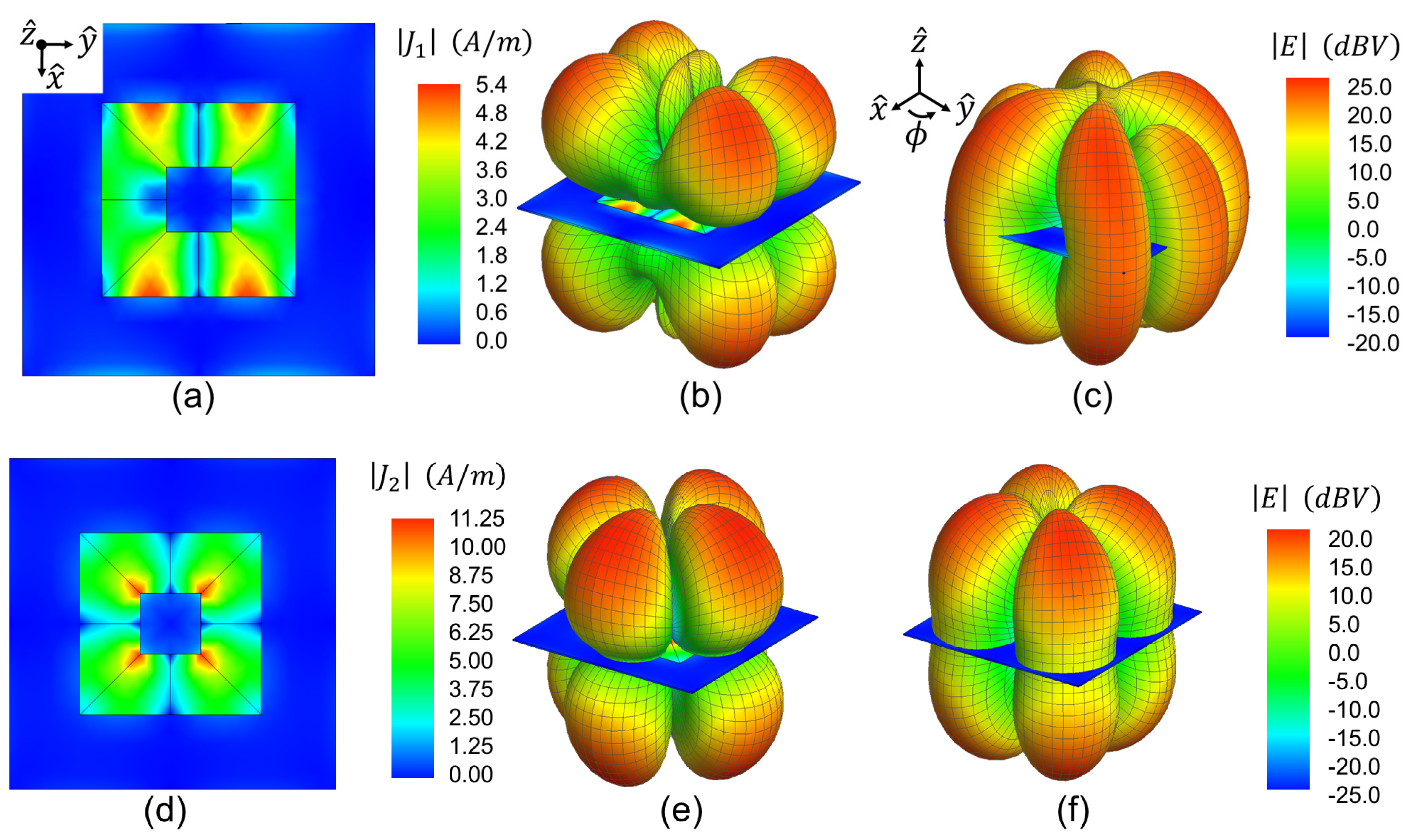
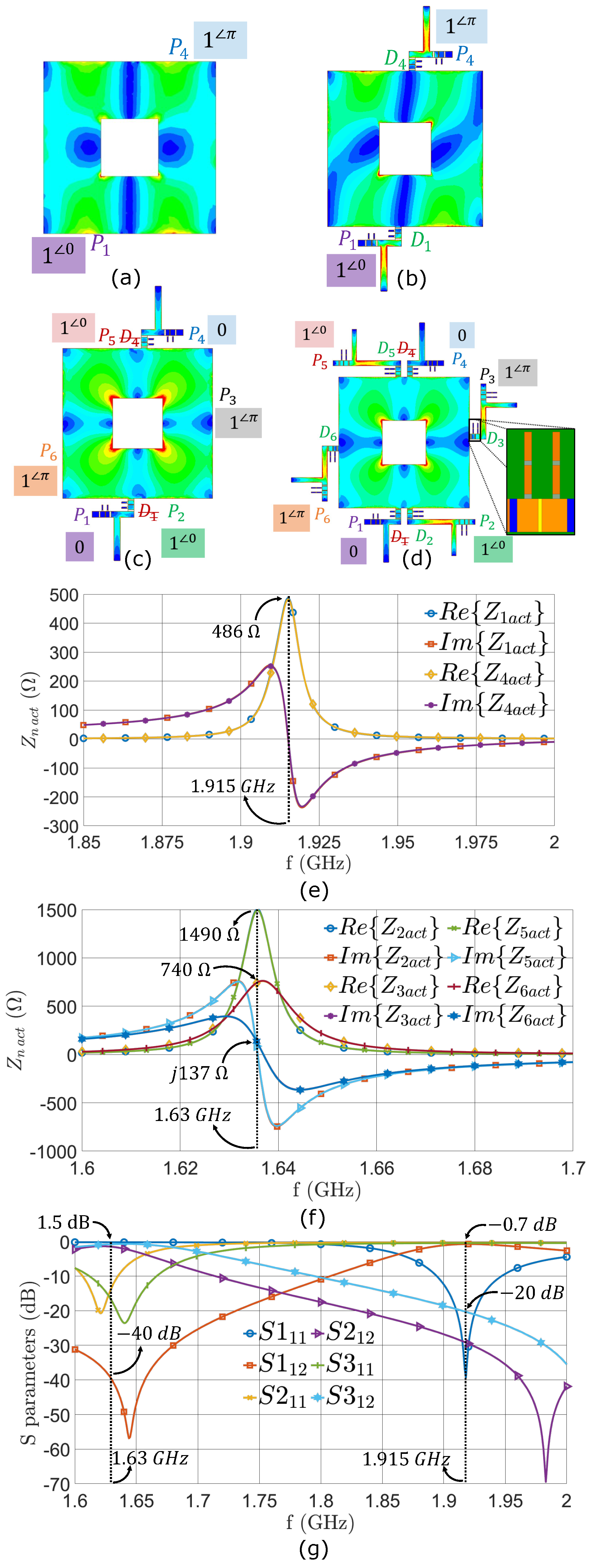
2. Characteristic Mode Analysis

Recently, antennas that adjust their response according to system and environmental requirements have been identified as a key technology in the development of cognitive radio. The required adaptability can be provided by electronically reconfigurable and multifunctional antennas and antenna arrays. As discussed in our introduction, the design of electrically compact multifunctional antennas is challenging, and in the majority of cases, complex designs are proposed to meet the high isolation requirements among the different bands of operation. These complex designs inherently suffer from high fabrication complexity (e.g., multilayer designs) and cost. In the past twenty years, several researchers (e.g., [36,37]) realized that eigenanalysis, specifically characteristic mode analysis, is a very powerful tool to study an arbitrary radiating geometry and design it appropriately. The key advantage of CMA over any other design method is represented by the insights into the physical characteristics of the geometry under study it provides. Namely, characteristic modes are real currents, I n = { J n , M n } (where J n corresponds to electric current, and M n , to magnetic current), that flow on the surface of the design. Characteristic modes are independent of excitation, since they are attained as the eigenfunctions of the generalized eigenvalue problem [38]:
[ X ] I n = λ n [ R ] I n
where [ R ] and [ X ] are the real and imaginary parts of the generalized impedance matrix, [ Z ] = [ R + j X ] , defined utilizing the appropriate operators [38], and λ n is the eigenvalue associated with the n th characteristic mode. Since these CMA currents are eigenfunctions, they form a set of orthogonal functions that can be used to expand the total current on the structure under study as
I = n V n I n 1 + j λ n
where V n = { V E , V M } is a known modal-excitation coefficient (where V E and V M are the modal-excitation coefficients related to electric and magnetic impinging waves, respectively); their definition can be found in [38]. Based on these current distributions, valuable information about the appropriate excitation (both the position and feed type) as well as the radiating characteristics, e.g., radiation pattern, polarization, etc., can be acquired. Finally, the eigensolution, λ n , informs us about the frequency of operation of the corresponding modes, while the term | 1 / ( 1 + j λ n ) | , known as modal significance, provides information about the radiation efficiency of the corresponding mode. Therefore, by appropriately utilizing characteristic mode analysis, any structure can be designed as a multifunctional antenna. The interested reader is referred to [17,27] for a comprehensive treatment of CMA.
Following the above, a characteristic mode analysis is performed on a square microstrip ring antenna using FEKO v2020 [39]. The ring is implemented on a square Rogers RT duroid 5880 substrate with ϵ r = 2.2 , t a n δ = 0.0009 , thickness of 1.5 mm, and edge length of 204.5 mm. The outer and inner edge lengths of the square ring are 112.5 mm and 37.5 mm, respectively. The magnitude of the characteristic current, | J n | , and θ ^ - and ϕ ^ -polarized radiations of the two desired characteristic modes are shown in Figure 1. The mode shown in Figure 1a at 1.9 GHz will be referred to as mode 1. Mode 1 has θ ^ -polarized radiation at ϕ = 0 in the broadside for θ ( 15 , 15 ) and ϕ = ± 45 planes for θ ( 25 , 60 ) , and ϕ ^ -polarized radiation at ϕ = 90 for θ ( 35 , 145 ) and ϕ = ± 45 planes for θ ( 25 , 155 ) , as shown in Figure 1b,c. The mode shown in Figure 1d at 1.6 GHz will be referred to as mode 2. Mode 2 has θ ^ -polarized radiation along the ϕ = 0 , 90 planes for θ ( 15 , 55 ) and ϕ ^ -polarized radiation along the ϕ = ± 45 planes for θ ( 15 , 55 ) , as shown in Figure 1e–f, respectively. Operation in these two modes provides nearly complete coverage of the upper hemisphere. Moreover, the physical properties of the radiation patterns of these two modes make them great candidates for monopulse tracking. Specifically, the fan beam of mode 1 in the broadside and the deep broadside null of mode 2 (along with the eight beams at ϕ = 0 and 45 planes) are the equivalent of sum and difference patterns of traditionally expensive phased arrays [35].

3. Feed Network Design

As mentioned in Section 2, CMA is performed in the absence of any excitation; however, the resulting characteristic currents provide valuable information about the appropriate excitation (e.g., its position and feed type). Based on this information, we excite the two desired modes with “ideal” excitation (i.e., lumped ports matched to the desired input impedance) and then apply matching methods to obtain a practically realizable design.

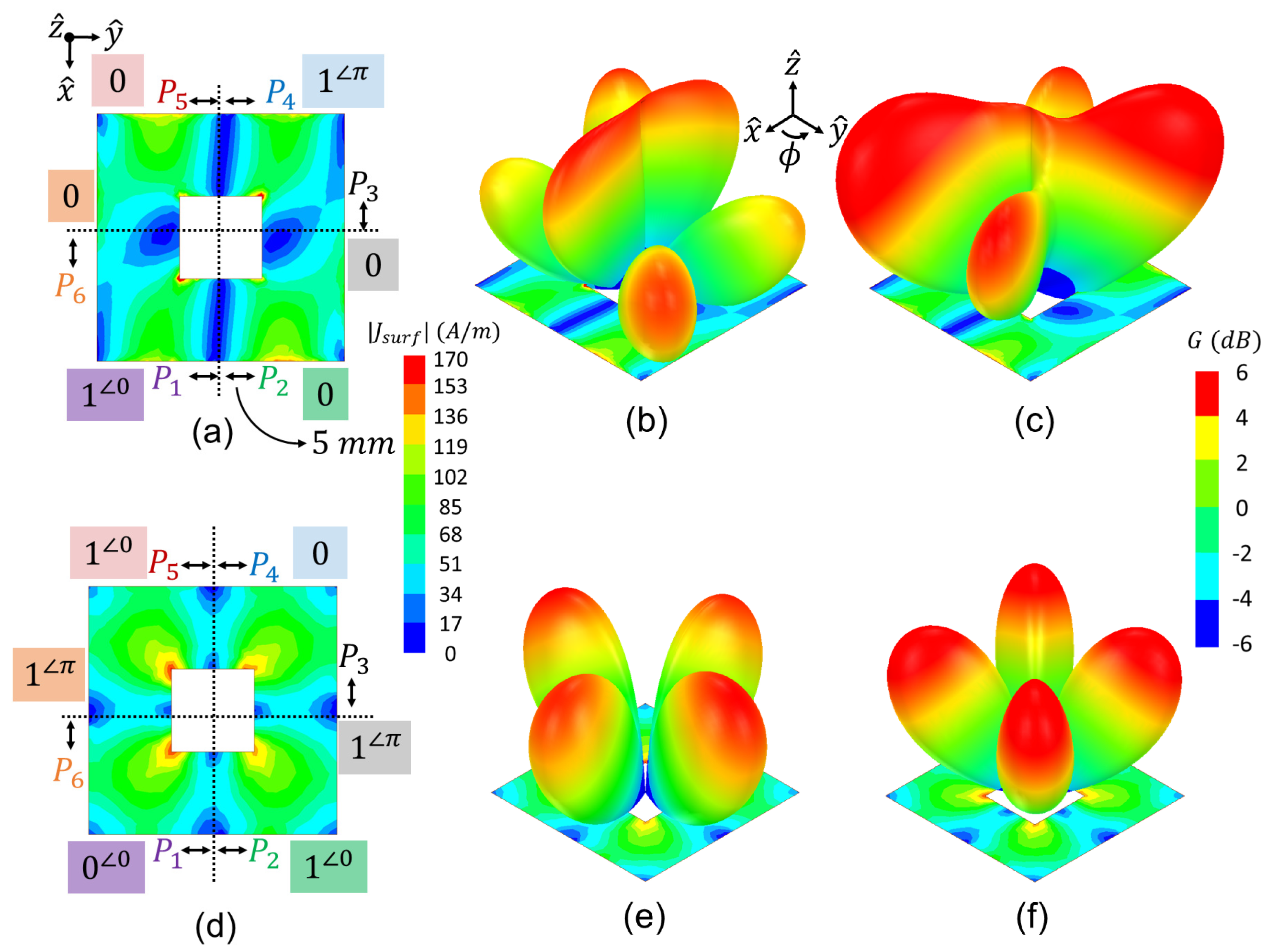
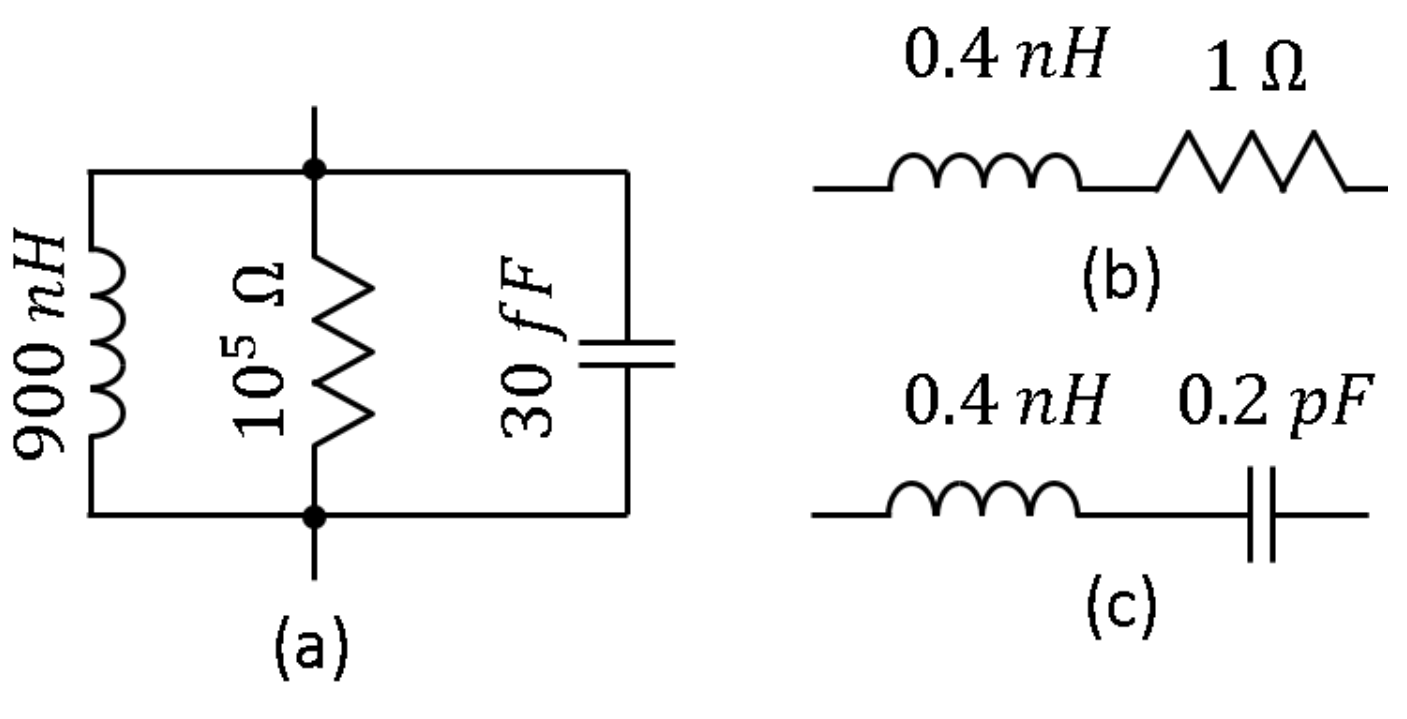
3.1. “Ideal” Mode Excitation Methods

The first step in the design of our antenna is the excitation of the two characteristic modes shown in Figure 1. Based on the characteristic currents, the positions of perfectly matched lumped ports are determined. Notably, ANSYS HFSS 2021 R2 is used as a full-wave simulator for this source-driven problem. Based on the current distribution of mode 1 (see Figure 1a), two differentially fed, symmetrically positioned ports, e.g., ports P 1 and P 3 in Figure 2a, are needed to produce the nulls along the x- and y-axes and excite mode 1. This is documented as configuration 1 in Table 1. Notably, coupling occurs between the ports. To account for this coupling, active parameters are used [40]. Thus, the voltage at the m th port of an N port antenna is given by
V 0 m = Z 0 I m + n = 1 N Z m n I n
where V 0 m is the desired excitation voltage of the m th port, Z 0 is the source impedance, Z m n is the mutual impedance between ports m and n for m n and the self-impedance when m = n , and I n is the unknown current flowing at the n th port. This defines N linear equations with N unknowns. Once the system has been solved, the active impedance of the m th port is given by
Z m , a c t = n = 1 N Z m n I n I m
Using the active impedance, a resonance is found at 1.9 GHz as expected according to the CMA. To efficiently excite the antenna, all the lumped ports are matched to the active input impedance at resonance. The distribution of surface electric current and the corresponding θ ^ - and ϕ ^ -polarized radiations are shown in Figure 2a–c, respectively. Notably, only the metalized square ring (without the substrate) is shown in these figures for clarity. The comparison between these figures and Figure 1a–c from the CMA indicates that mode 1 is strongly excited by configuration 1. The only discernible difference is that configuration 1 does not strongly produce the ϕ ^ -polarized-radiation lobe on the ϕ = 90 plane (compare Figure 1c and Figure 2c). This difference is attributed to the fact that configuration 1 slightly excites other modes on the ring. This is evidenced by the strong currents at the inner edges of the ring, shown in the inset of Figure 2a, which ideally should not be present in mode 1 (see Figure 1a). Finally, the radiation efficiency of our simulated antenna for configuration 1 is 83.5 % , which agrees very well with the predicted modal significance of nearly unity in our CMA.
To excite characteristic mode 2, one may be tempted to generate the nulls along the x- and y-axes using two pairs of orthogonal differentially fed ports, e.g., by differentially feeding ports P 1 and P 3 and differentially feeding ports P 2 and P 3 . However, this configuration excites two orthogonal mode 1 radiations. To correctly excite mode 2, adjacent ports must be 180 out-of-phase. For convenience, this is denoted as configuration 2 in Table 1. Using the active impedance, a resonance is found at 1.6 GHz, and this agrees with the CMA predictions. The lumped ports are matched to the active input impedance at resonance to efficiently excite the antenna. The distribution of surface electric current and the corresponding θ ^ - and ϕ ^ -polarized radiations are shown in Figure 2d–f, respectively. Comparing Figure 2d–f with Figure 1d–f from the CMA clearly shows that configuration 2 strongly excites mode 2. Furthermore, the radiation efficiency of our simulated antenna for configuration 2 is 90.7 % , which agrees very well with the predicted modal significance of nearly unity in our CMA.

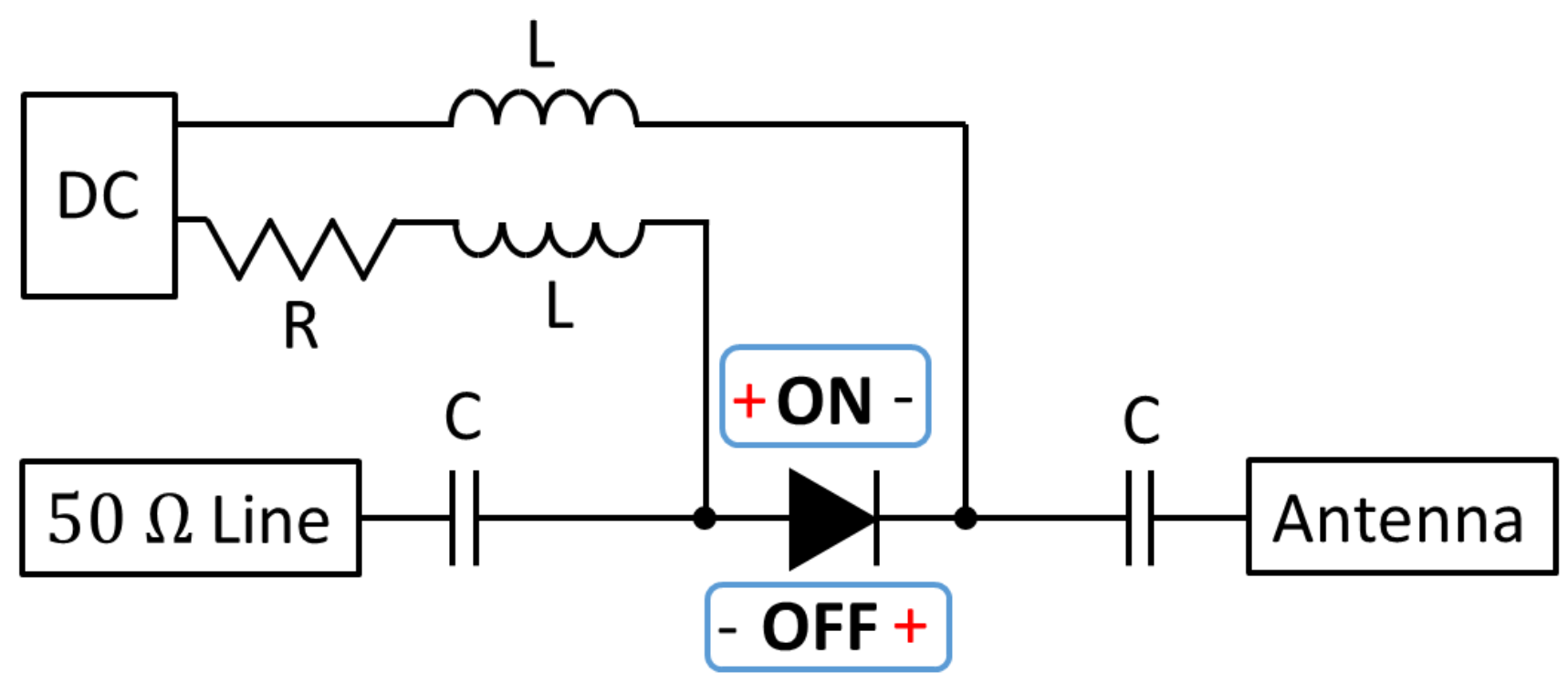
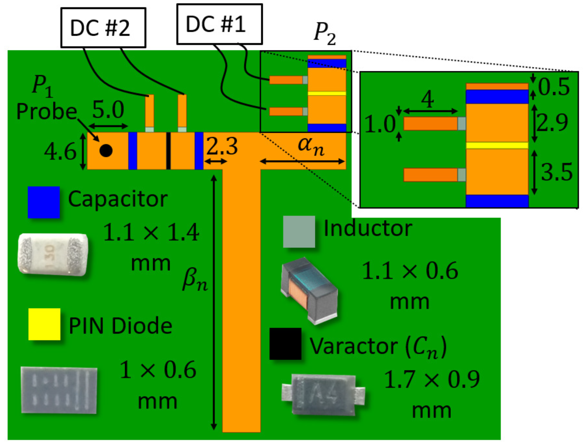
3.2. Feed Network Design

As discussed above, after we establish the excitation of the desired modes, the next step is to design the required feed network for our antenna. The active input impedance values for configurations 1 and 2 (see Table 1) are 555 Ω and 1146 Ω at 1.9 GHz and 1.6 GHz, respectively. To proceed, the type of matching network must be chosen. There are two approaches that can be followed: (a) designing a wide-band or dual-band matching network that supports the desired bands and (b) designing two different matching networks, each dedicated to the corresponding configuration. Designing a static dual-band matching network that supports a change in impedance of over 2:1 is challenging, and limited such works exist in the literature. One notable example is the dual-band single-stub network proposed in [41]. However, given the above impedance values, a network following [41], or similar approaches, would require lines with high impedance (over 170 Ω ), making it extremely challenging to fabricate with traditional PCB technology and stubs with low impedance (below 20 Ω ), which can perturb the modes of the antenna due to coupling.
This problem can be addressed by designing a separate matching network for each configuration of our antenna. Therefore, a set of ports are dedicated to configuration 1, and another set of ports are dedicated to configuration 2. However, as shown in Figure 2a,d, both configurations 1 and 2 use ports P 1 and P 3 . To address this and preserve symmetry, two new ports are introduced for configuration 1; they are slightly rotated counterclockwise and denoted as ports P 1 and P 4 in Figure 3a. Conversely, the four dedicated ports of configuration 2 are slightly rotated clockwise and are denoted as ports P 2 , P 3 , P 5 , and P 6 in Figure 3d. As shown in Figure 3a,d, these rotations separate the previously overlapping dedicated ports by 10 mm. For convenience, the dedicated configurations are tabulated in Table 2, which shows which port is used in each configuration. These slight changes in the port locations for the two configurations do not significantly change their current distributions, because these distributions are symmetric. For configuration 1, this is validated by comparing Figure 3a–c to Figure 1a–c. For configuration 2, this is validated by comparing Figure 3d–f to Figure 1d–f. These comparisons confirm that our two dedicated configurations (shown in Table 2) strongly excite characteristic modes 1 and 2.
Next, a dedicated matching network can be designed and connected to each port. To mitigate the effects of the matching networks, PIN diodes are used to “connect” and “disconnect” the networks dedicated to configurations 1 and 2. These PIN diodes are placed in series with the matching network as close as possible to the edge of the ring to preserve the original geometry analyzed with CMA.
For simplicity, single-stub matching networks with 50 Ω lines are used [42]. The PIN diode is turned ON (forward-biased) and OFF (reverse-biased) by the biasing network shown in Figure 4. The biasing network consists of inductors (which act as RF chokes), DC-blocking capacitors, and a current-limiting resistor. Specifically, the biasing network consists of two 0402DF-901XJR 900 nH inductors by Coilcraft [43], one BAP55LX PIN diode by NXP [44], two 0805N130 13 pF capacitors by PPI [45], and a standard through-hole 100 Ω resistor. The PIN diode is switched ON with a 2.4 V DC power supply, which provides sufficient current [44]. The PIN diode is switched OFF by just turning off the DC power supply, since reverse biasing does not provide any advantage (i.e., it does not significantly increase isolation) [44].
According to [43], in the 1–2 GHz frequency range, an inductor is modeled as a parallel combination of 900 nH inductance, 30 fF capacitance, and 10 5 Ω resistance, as shown in Figure 5a. In this band, according to [44], the PIN diode is modeled as an inductor in series with either a 1 Ω resistor, when ON (refer to Figure 5b), or a 0.2 pF capacitor, when OFF (refer to Figure 5c). Also, in this band, according to [45], a DC blocking capacitor is modeled with an ideal capacitance value of 13 pF. Following the above, appropriate RLC boundary conditions are defined in HFSS to model these lumped components.
The PIN diode in the series configuration (see Figure 4) only provides ∼6 dB isolation in the OFF state in the 1–2 GHz band. This isolation is sufficient for properly exciting the two configurations (each configuration generates one of the desired modes), but the remaining coupling between the matching networks of the two configurations causes the radiation efficiency of the two modes to be less than 50 % . To improve this isolation, multiple PIN diodes can be used in series. Alternatively, in this work, a more elegant approach is developed. It is well known that an open-circuited quarter-wavelength stub can be used as a band-stop filter [42]. It follows that isolation can be increased by adding a λ 1 / 4 stub to configuration 2 matching networks and a λ 2 / 4 stub to configuration 1 matching networks, where λ 1 and λ 2 are the resonant frequencies of configurations 1 and 2, respectively. However, additional stubs increase the size of each matching network, thereby perturbing the ring antenna and preventing configurations 1 and 2 from properly exciting modes 1 and 2.
A better approach is to constrain the length of the single stub of the matching network, i.e., constrain the single stubs of the configuration 1 and 2 matching networks to be ∼ λ 2 / 4 and ∼ λ 1 / 4 , respectively. Under these constraints, the reactance of the stub is generally insufficient for the network to match 50 Ω . To correct this, additional reactance is added to the matching network. Specifically, in simulation, the SMV 1405 varactor [46] (0.5–2.5 pF) is used for all the matching networks. Notably, varactors are used to tune the fabricated design instead of fixed capacitors. The same biasing network used for the PIN diode (see Figure 4) is also used to tune the varactor. Based on the above, the single-stub matching network design used for both configurations is shown in Figure 6. This network consists of two geometric parameters, α n , β n , and the capacitance of the varactor, C n . Notably, a 90 bend is used to reduce coupling between adjacent ports (ports P 1 and P 2 , and ports P 4 and P 5 in Figure 3a). Furthermore, as shown in Figure 6, the matching network is fed with a probe so that the feed network does not have to be connected to the edge of the substrate for feeding. Using the feed network in Figure 6, the ports of both configurations are matched to 50 Ω . As discussed in the following, the matching network is optimized for the active input impedance of each configuration.
Configuration 1, where ports P 1 and P 4 are differentially fed (as shown in Table 2), generates the current distribution indicated in Figure 7a. The active input impedance, Z a c t , shown in Figure 7e, indicates a sharp resonance corresponding to characteristic mode 1. The parameters of the matching network in Figure 6 are correspondingly adjusted and are denoted by “network 1” in Table 3. The S parameters of this matching network are shown in Figure 7g, where S m i j denotes the S parameter for the m th matching network. The S 1 11 curve in Figure 7g shows a 10 dB return loss, and the S 1 12 curve indicates a 0.7 dB insertion loss. Furthermore, the S 1 12 curve shows 40 dB isolation at the resonant frequency of configuration 2 (∼1.6 GHz). This matching network is added to the antenna, and the magnitude of the electric current distribution is shown in Figure 7b, while the θ ^ - and ϕ ^ -polarized radiations are shown in Figure 8a,g, respectively.
Configuration 2 (see Table 2) is excited when PIN diodes D1 and D2 are turned OFF, and it generates the current distribution indicated in Figure 7c. The active input impedance, Z a c t , in Figure 7f shows that ports P 2 and P 5 have different input impedance from ports P 3 and P 6 due to the asymmetry introduced because of the configuration 1 matching network. The parameters of the matching network for ports P 2 and P 5 are denoted by “network 2” in Table 3, while the parameters of the matching network for ports P 3 and P 6 are denoted by “network 3”. Due to the high input impedance of configuration 2, the RF choke is composed of two series inductors as opposed to one (refer to the zoomed portion of Figure 7d). The S 2 11 and S 3 11 curves in Figure 7g show that 10 dB matching is achieved for both pairs of ports, and the S 2 12 and S 3 12 curves indicate an insertion loss below 1.5 dB. Additionally, these curves indicate that isolation greater than 20 dB is achieved at the resonant frequency of configuration 1, ∼1.9 GHz. These matching networks are added to the antenna, and the magnitude of the electric current distribution is shown in Figure 7d, while the θ ^ - and ϕ ^ -polarized radiations are shown in Figure 8d,j, respectively. Notably, with these matching networks, modes 1 and 2 are excited with similar radiation efficiency values, 66.8 % and 71 % , respectively. The simulated active S parameters of configurations 1 and 2 (defined in Table 2 and Table 4), S S 1 a c t and S S 2 a c t , respectively, for the finalized design (see Figure 7d) are shown in Figure 9.
Finally, it is important to emphasize that due to the intense concentration of fields of both modes, e.g., mode 2 has strong fields confined to the inner vertices (refer to Figure 1d), their radiation efficiency is sensitive to dielectric losses. To quantify this sensitivity, the radiation efficiency values of configurations 1 and 2, denoted by η C 1 and η C 2 , respectively, are tabulated in Table 5, where the relative permittivity is 2.2 and the dielectric loss tangent is varied in the range of values commonly found in substrates. Notably, these results are obtained using matched lumped ports and so do not account for insertion losses of the feed network. The data indicate that the ring antenna cannot be implemented on popular substrates like FR4, with t a n δ = 0.02 , which presents a practical problem. Notably, to address this problem, an air gap of 0.738 mm between the ground and substrate can be added when the ring is fabricated on a 0.762 mm thick Rogers Kappa 438. In this case, configurations 1 and 2 have radiation efficiency values of 86 % and 90 % , respectively.

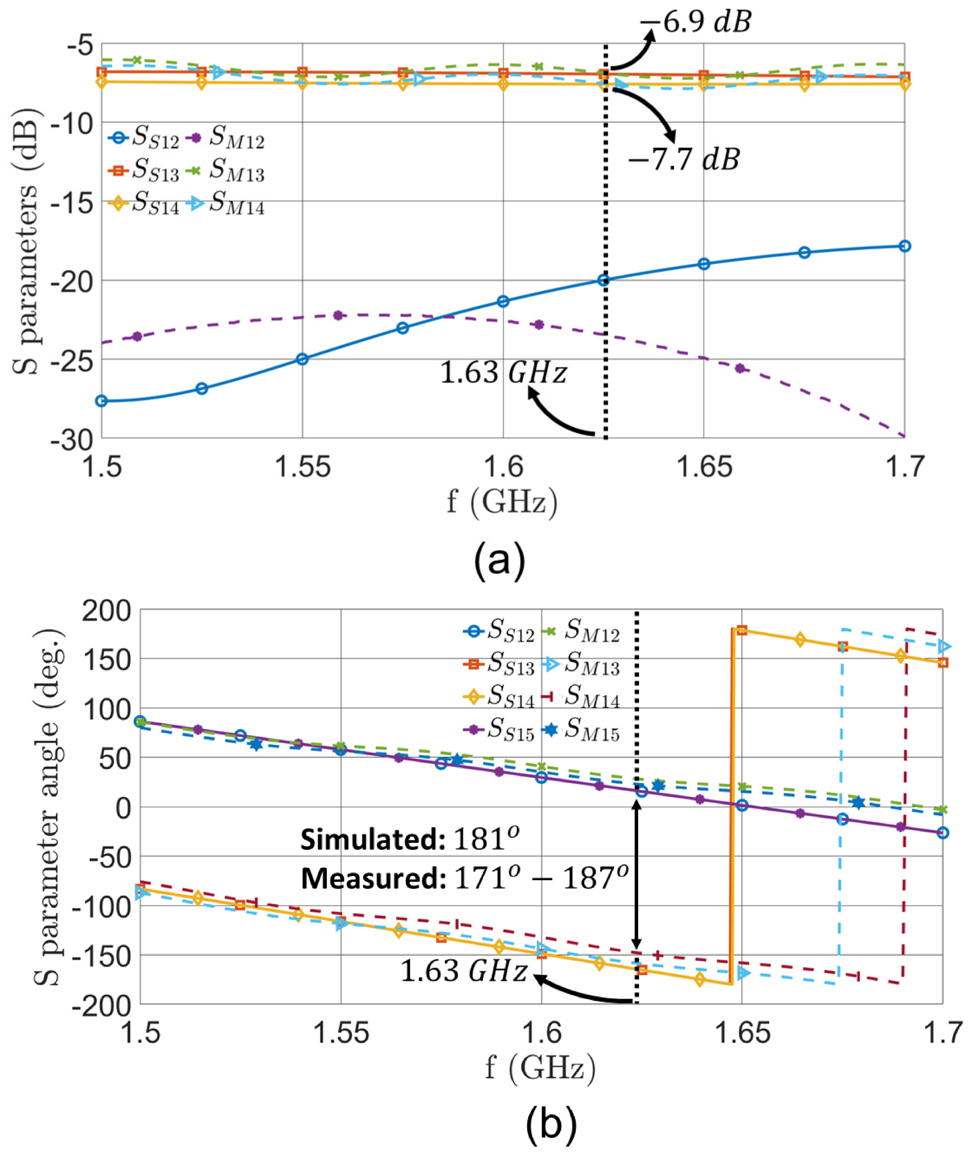
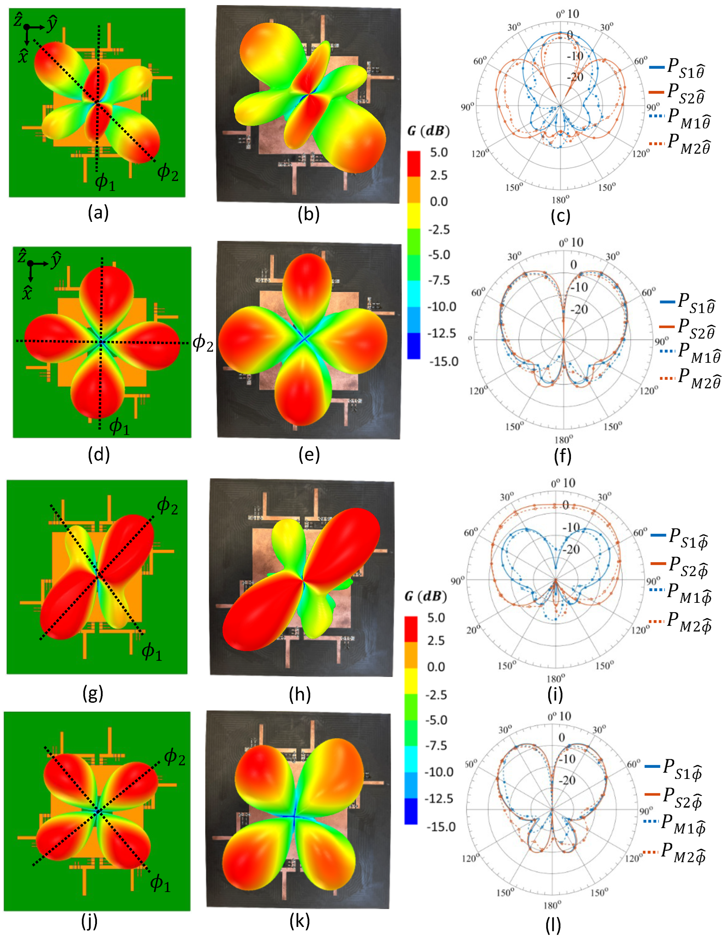
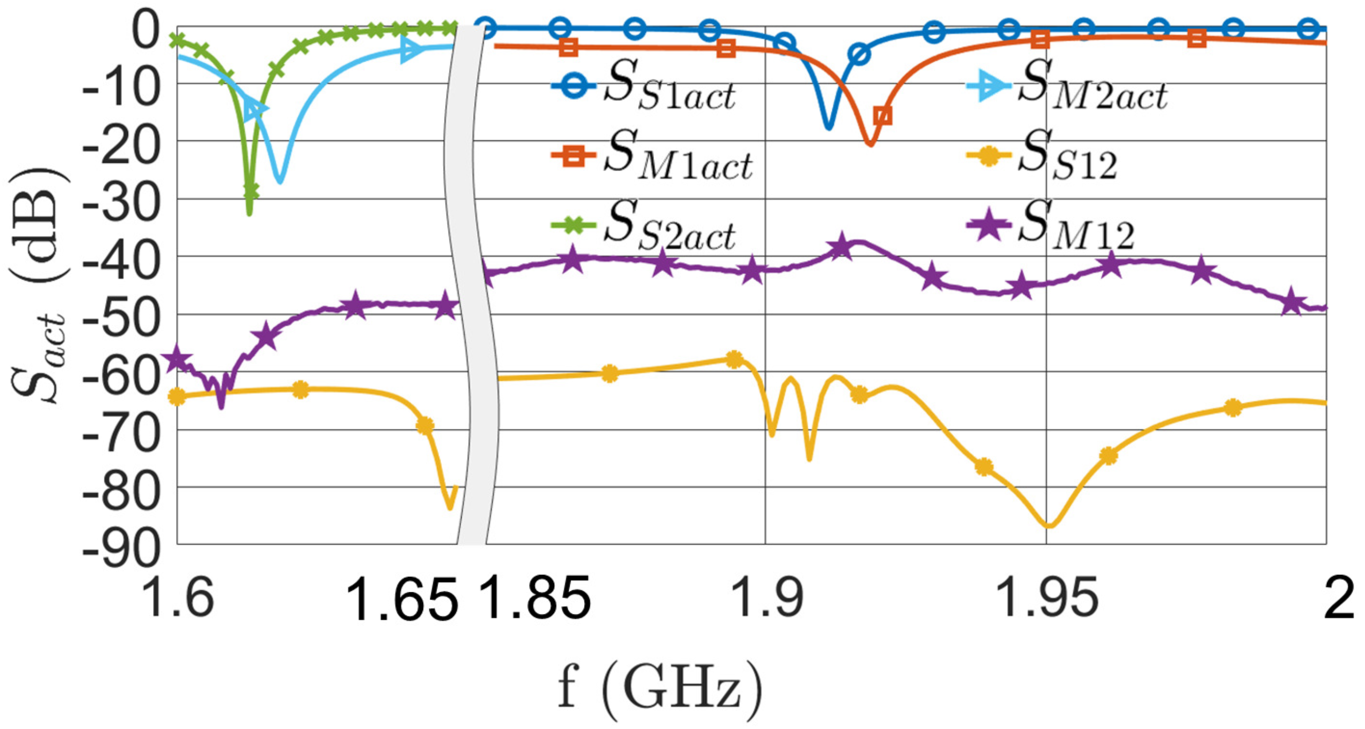
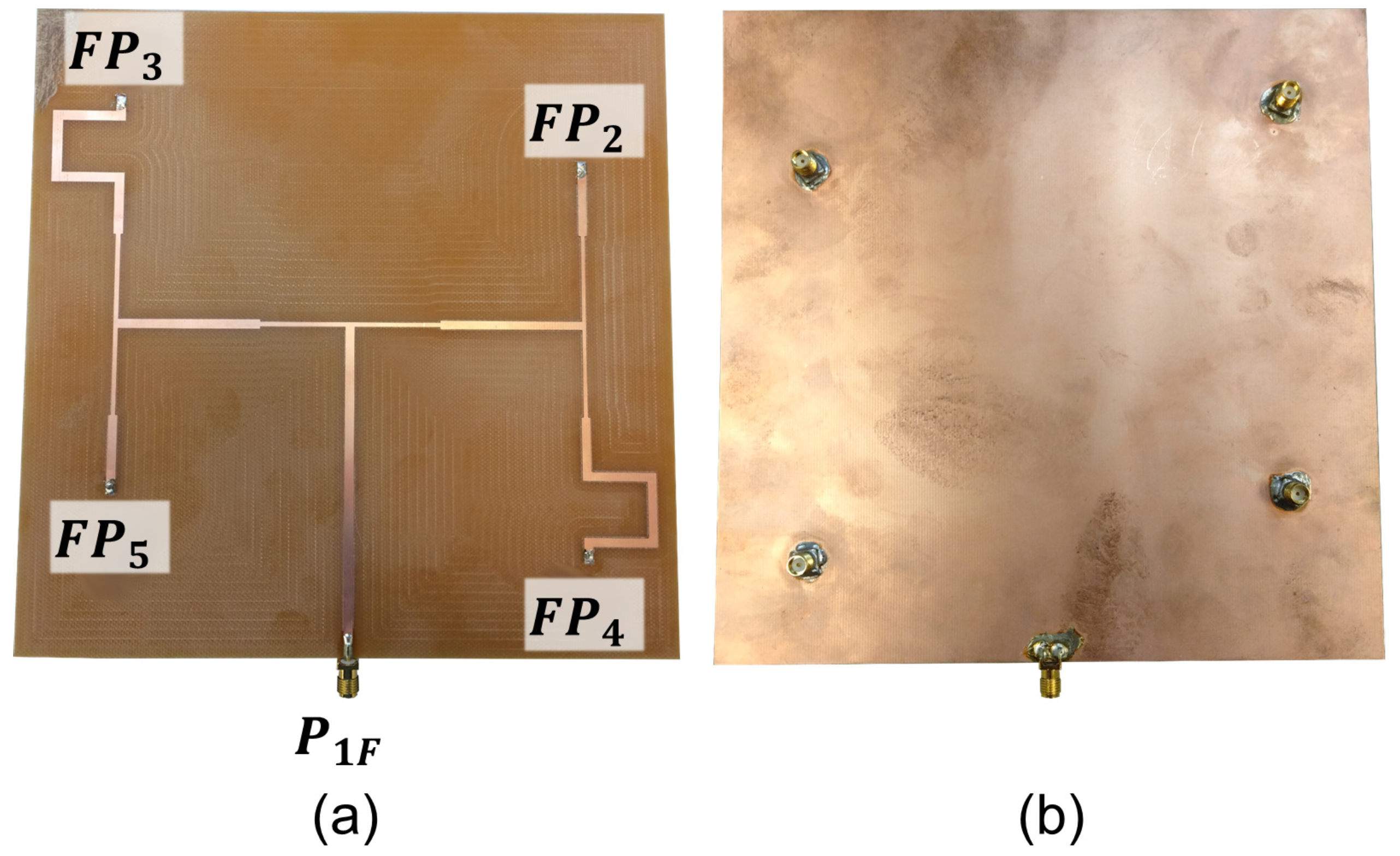
4. Fabrication and Measurement

In this section, the feed networks for configurations 1 and 2 are initially discussed. Then, the fabrication and measurements of the antenna are reported, and the latter are compared with the simulations. Configuration 1 (see Table 2) was implemented using a 3 dB 180 hybrid coupler by Clear Microwave Inc., model # DS-4D00 [47]. Configuration 2 (see Table 2) was implemented using a custom four-way microstrip power divider. The divider consisted of three identical T-Junction power dividers, each one with 50 Ω input and two 70.7 Ω quarter-wave transformers as output, which connected to two 50 Ω lines. Meandering was used to achieve the appropriate phasing between ports. The divider was fabricated on 1.5 mm thick FR4 using an LPKF S103 milling machine, and it is shown in Figure 10. The S parameters were measured using an Agilent E5071C VNA. The simulated and measured S parameters are compared in Figure 11. At the resonant frequency of configuration 2 (i.e., 1.63 GHz), Figure 11a indicates that there is less than a 0.25 dB difference between simulated and measured magnitude. Additionally, Figure 11b shows that in simulation, adjacent ports are 181 out-of-phase, while in measurement, adjacent ports are 171–187 out-of-phase at 1.63 GHz.
The ring antenna was fabricated and measured using the same equipment as the feed network, and it is shown in Figure 12. To minimize the effects of the DC biasing cables for the PIN diodes and varactors, the cables were connected from the bottom side of the substrate, as shown in Figure 12b. The measured active S parameter when the ring antenna was fed for configuration 1, using the 3 dB 180 hybrid coupler [47], is shown as S M 1 a c t in Figure 9. Good agreement is observed between simulated and measured S parameters in Figure 9. Notably, due to fabrication errors, the SMV 1405 ( 0.5 2.5 pF) varactor was replaced with an SMV 1413 (2–10 pF) in the matching network for mode 1 to achieve good matching. Matching was found to be the best when both varactors were set to 10 pF. Additionally, Figure 9 shows that the simulated bandwidth is 7 MHz ( 0.4%), while the measured bandwidth is 16.8 MHz ( 1%). This bandwidth is sufficient for operation in bands 33 and 37 of the 3rd Generation Partnership Project (3GPP) Evolved Universal Terrestrial Radio Access (E-UTRA) bands, which have bandwidths of 20 MHz [48]. Notably, the narrow bandwidth of both modes is expected, as the microstrip ring antenna is formed by a geometrical perturbation of the well-known high-Q microstrip patch antenna. The bandwidth of the microstrip ring can be enhanced with traditional techniques that modify the geometry of the radiating structure and/or the feed network. Additionally, due to the high isolation between the ports in configurations 1 and 2, the ports in configuration 2 can be left open, or they can be matched to 50 Ω for this measurement with little difference.
The measured active S parameter when the ring antenna was fed for configuration 2 (using the four-way power divider in Figure 10 and Figure 11) is shown as S M 2 a c t in Figure 9. The best matching was achieved when the varactors of the configuration 2 network provided 2.5 pF capacitance, as opposed to the 2 pF capacitance used in simulation. The results in Figure 9 show that the operational frequency of the prototyped antenna is slightly higher than the simulated one (by 4.2 MHz). Also, the simulated and measured bandwidths are 4.2 MHz ( 0.2%) and 11.2 MHz ( 0.5%), respectively. These bandwidths are sufficient for land mobile satellite operations [49], which typically require a bandwidth of 7 MHz. Notably, the small bandwidth of configurations 1 and 2 is expected based on [31,32]. Finally, Figure 9 indicates that there is high isolation between the two modes. Specifically, the simulated and measured isolation values are 58 dB and 37 dB, respectively. This difference is attributed to fabrication errors.
The radiation of the fabricated antenna was measured using the MVG near-field Starlab anechoic chamber at Florida International University (FIU). Under configuration 1, the top view of the 3D simulated θ ^ - and ϕ ^ -polarized radiations is shown in Figure 8a,g, respectively. The corresponding measured θ ^ - and ϕ ^ -polarized radiations are shown in Figure 8b,h, respectively.
For further comparison between simulations and measurements, the radiation patterns in two key elevation planes are shown. On the n th elevation plane, where n [ 1 , 2 ] , the simulated and measured patterns for polarization p ^ [ θ ^ , ϕ ^ ] are denoted as P S n p ^ and P M n p ^ , respectively. For the θ ^ -polarized radiation, the two key planes at ϕ 1 = 0 and ϕ 2 = 45 (indicated by dashed lines in Figure 8a) are used, and the corresponding patterns are plotted in Figure 8c. For the ϕ ^ -polarized radiation, the two key planes at ϕ 1 = 20 and ϕ 2 = 140 are used (indicated by dashed lines in Figure 8g), and the corresponding patterns are plotted in Figure 8i. The comparisons of these patterns indicate that simulated and measured results for configuration 1 agree very well.
For configuration 2, the top view of the 3D simulated θ ^ - and ϕ ^ -polarized radiations are shown in Figure 8d,j, respectively. The corresponding measured θ ^ - and ϕ ^ -polarized radiations are shown in Figure 8e,k, respectively. For the θ ^ -polarized radiation, two key planes at ϕ 1 = 0 and ϕ 2 = 90 are chosen, as shown in Figure 8d, and the corresponding patterns are shown in Figure 8f. For the ϕ ^ -polarized radiation, two key planes at ϕ 1 = 40 and ϕ 2 = 130 are chosen, as shown Figure 8j, and the corresponding patterns are shown in Figure 8l. The comparisons of these patterns indicate that the simulated and measured results for configuration 2 agree very well.
Finally, it is important to emphasize that the measured patterns for both configurations in Figure 8 have been adjusted to include the losses. Specifically, for configuration 1, the total insertion loss due to cables and the 3 dB 180 hybrid coupler [47] was measured and found to be approximately 1 dB. Therefore, the measured peak gain and radiation efficiency are 4.7 dB and 44.3 % , respectively. Hence, compared with the simulations, the measured results have 1 dB lower peak gain and 22.2 % lower radiation efficiency. This discrepancy is expected due to the fabricated antenna requiring 8.5 pF more capacitance than in simulation due to fabrication errors. Under configuration 2, the total insertion loss due to cables and the fabricated feed network was measured and found to be approximately 3 dB (refer to Figure 11a). Therefore, the measured peak gain and radiation efficiency are 4.7 dB and 64 % , respectively. Hence, the simulated and measured peak gain and radiation efficiency agree very well. This is expected because the fabricated antenna only required 0.5 pF higher capacitance compared with the simulations. Notably, the measured gain of 4.7 dB falls into the expected range of traditional monolayer antennas [50].
To elucidate the advantages of our work over similar state-of-the-art dual-mode dual-band antenna designs with dedicated feed networks, Table 6 compares the measured bandwidth ( B W ), peak realized gain ( G p ; gain that incorporates all losses, e.g., reflection and substrate losses), minimum in-band isolation ( I m i n ), and radiation efficiency ( η ), for both the low band (LB) and high band (HB) of operation. In this work, configuration 2 corresponds to the low band, while configuration 1 corresponds to the high band. Table 6 shows that the main advantage of our proposed work lies in its ability to simultaneously reconfigure its radiation pattern and frequency of operation using a single multimode radiator. Furthermore, Table 6 demonstrates that our proposed design achieves this reconfigurability while simultaneously attaining the isolation, gain, and bandwidth of state-of-the-art non-reconfigurable designs.

5. Conclusions

In this work, an electronically reconfigurable multimode antenna was designed based on CMA. Specifically, CMA was applied to a square microstrip ring antenna, revealing higher-order orthogonal modes. As a proof of concept, an antenna was designed for two of these modes, and an electronically reconfigurable feed network based on PIN diodes was developed to switch between the two modes. The design was validated with fabrication and measurements. Both simulations and measurements demonstrated the complementary radiation patterns of modes 1 and 2, which can act as sum and difference beams. This makes the proposed antenna a good candidate for low-monopulse radar tracking, which is a more cost-effective solution than traditionally expensive phased arrays [35]. Notably, the reduced cost of a system based on our proposed reconfigurable antenna is achieved with an inherent reduction in performance as compared with a system based on non-reconfigurable antennas optimized to operate in a single band or mode of operation.
Importantly, this work has demonstrated how the physical insights gained with CMA can be applied to antenna geometries in a systematic way to create novel low-profile and compact antennas.

Author Contributions

Conceptualization, N.E.R. and C.L.Z.; methodology, N.E.R. and C.L.Z.; software, N.E.R. and C.L.Z.; validation, N.E.R. and C.L.Z.; formal analysis, N.E.R. and C.L.Z.; investigation, N.E.R. and C.L.Z.; resources, S.V.G.; data curation, N.E.R. and C.L.Z.; writing—original draft preparation, N.E.R. and C.L.Z.; writing—review and editing, N.E.R., C.L.Z. and S.V.G.; visualization, N.E.R., C.L.Z. and S.V.G.; supervision, C.L.Z. and S.V.G.; project administration, C.L.Z. and S.V.G.; funding acquisition, S.V.G. All authors have read and agreed to the published version of the manuscript.

Funding

This research was funded by Air Force Office of Scientific Research Grants FA9550-18-1-0191 and FA9550-19-1-0290.

Data Availability Statement

Not applicable.

Conflicts of Interest

The authors declare no conflict of interest.

References

  1. Hong, W. Solving the 5G Mobile Antenna Puzzle: Assessing Future Directions for the 5G Mobile Antenna Paradigm Shift. IEEE Microw. Mag. 2017, 18, 86–102. [Google Scholar] [CrossRef]
  2. Rowell, C.; Lam, E.Y. Mobile-Phone Antenna Design. IEEE Antennas Propag. Mag. 2012, 54, 14–34. [Google Scholar] [CrossRef]
  3. Zhang, Y.; Zhang, S.; Li, J.; Pedersen, G.F. A Transmission-Line-Based Decoupling Method for MIMO Antenna Arrays. IEEE Trans. Antennas Propag. 2019, 67, 3117–3131. [Google Scholar] [CrossRef]
  4. Yang, F.; Rahmat-Samii, Y. Microstrip antennas integrated with electromagnetic band-gap (EBG) structures: A low mutual coupling design for array applications. IEEE Trans. Antennas Propag. 2003, 51, 2936–2946. [Google Scholar] [CrossRef]
  5. Liu, D.Q.; Luo, H.J.; Zhang, M.; Wen, H.L.; Wang, B.; Wang, J. An Extremely Low-Profile Wideband MIMO Antenna for 5G Smartphones. IEEE Trans. Antennas Propag. 2019, 67, 5772–5780. [Google Scholar] [CrossRef]
  6. Li, M.; Zhong, B.G.; Cheung, S.W. Isolation Enhancement for MIMO Patch Antennas Using Near-Field Resonators as Coupling-Mode Transducers. IEEE Trans. Antennas Propag. 2019, 67, 755–764. [Google Scholar] [CrossRef]
  7. Gao, D.; Cao, Z.X.; Fu, S.D.; Quan, X.; Chen, P. A Novel Slot-Array Defected Ground Structure for Decoupling Microstrip Antenna Array. IEEE Trans. Antennas Propag. 2020, 68, 7027–7038. [Google Scholar] [CrossRef]
  8. Zhang, Y.; Zhang, S.; Li, J.; Pedersen, G.F. A Wavetrap-Based Decoupling Technique for 45° Polarized MIMO Antenna Arrays. IEEE Trans. Antennas Propag. 2020, 68, 2148–2157. [Google Scholar] [CrossRef]
  9. Xu, H.; Gao, S.S.; Zhou, H.; Wang, H.; Cheng, Y. A Highly Integrated MIMO Antenna Unit: Differential/Common Mode Design. IEEE Trans. Antennas Propag. 2019, 67, 6724–6734. [Google Scholar] [CrossRef]
  10. Priya, S.; Dwari, S.; Kumar, K.; Mandal, M.K. Compact self-quadruplexing SIW cavity-backed slot antenna. IEEE Trans. Antennas Propag. 2019, 67, 6656–6660. [Google Scholar] [CrossRef]
  11. Sun, L.; Li, Y.; Zhang, Z.; Feng, Z. Wideband 5G MIMO Antenna With Integrated Orthogonal-Mode Dual-Antenna Pairs for Metal-Rimmed Smartphones. IEEE Trans. Antennas Propag. 2020, 68, 2494–2503. [Google Scholar] [CrossRef]
  12. Ren, A.; Liu, Y.; Sim, C.-Y.-D. A Compact Building Block With Two Shared-Aperture Antennas for Eight-Antenna MIMO Array in Metal-Rimmed Smartphone. IEEE Trans. Antennas Propag. 2019, 67, 6430–6438. [Google Scholar] [CrossRef]
  13. Jha, K.R.; Bukhari, B.; Singh, C.; Mishra, G.; Sharma, S.K. Compact Planar Multistandard MIMO Antenna for IoT Applications. IEEE Trans. Antennas Propag. 2018, 66, 3327–3336. [Google Scholar] [CrossRef]
  14. Chu, L.J. Physical Limitations of Omni-Directional Antennas. J. Appl. Phys. 1948, 19, 1163–1175. [Google Scholar] [CrossRef]
  15. Ehrenborg, C.; Gustafsson, M.; Capek, M. Capacity Bounds and Degrees of Freedom for MIMO Antennas Constrained by Q-Factor. IEEE Trans. Antennas Propag. 2021, 69, 5388–5400. [Google Scholar] [CrossRef]
  16. Ehrenborg, C.; Gustafsson, M. Physical Bounds and Radiation Modes for MIMO Antennas. IEEE Trans. Antennas Propag. 2020, 68, 4302–4311. [Google Scholar] [CrossRef]
  17. Garbacz, R.J. A Generalized Expansion for Radiated and Scattered Fields. Ph.D. Dissertation, Department of Electrical and Computer Engineering, Electrical and Computer Engineering, Colombus, OH, USA, 1968. [Google Scholar]
  18. Harrington, R.F.; Mautz, J.R. Theory of Characteristic Modes for Conducting Bodies. IEEE Trans. Antennas Propag. 1971, 19, 622–628. [Google Scholar] [CrossRef]
  19. Harrington, R.; Mautz, J. Computation of characteristic modes for conducting bodies. IEEE Trans. Antennas Propag. 1971, 19, 629–639. [Google Scholar] [CrossRef]
  20. Cabedo, M.; Antonino, E.; Valero, A.; Ferrando, M. The Theory of Characteristic Modes Revisited: A Contribution to the Design of Antennas for Modern Applications. IEEE Antennas Propag. Mag. 2007, 49, 52–68. [Google Scholar] [CrossRef]
  21. Cheng, H.; Xiao, G.; Wang, X. A Low-Profile Wideband Patch Antenna With Modified Parasitic Mushroom Structures on Nonperiodic AMC. IEEE Antennas Wirel. Propag. Lett. 2023, 22, 719–723. [Google Scholar] [CrossRef]
  22. Zhang, Z.; Cheng, Y.; Luo, H.; Chen, F. Low-Profile Wideband Circular Polarization Metasurface Antenna With Characteristic Mode Analysis and Mode Suppression. IEEE Antennas Wirel. Propag. Lett. 2023, 22, 898–902. [Google Scholar] [CrossRef]
  23. Jiang, F.; Zhang, Z.; Li, M.; Shen, S.; Chiu, C.Y.; Zhang, Y.; Cheng, Q.S.; Murch, R. Multiport Pixel Antenna Optimization Using Characteristic Mode Analysis and Sequential Feeding Port Search. IEEE Trans. Antennas Propag. 2022, 70, 9160–9174. [Google Scholar] [CrossRef]
  24. Adams, J.J.; Genovesi, S.; Yang, B.; Antonino-Daviu, E. Antenna Element Design Using Characteristic Mode Analysis: Insights and research directions. IEEE Antennas Propag. Mag. 2022, 64, 32–40. [Google Scholar] [CrossRef]
  25. Liu, N.-W.; Huang, B.-B.; Zhu, L.; Fu, G. Isolation and Bandwidth Improvements of Multimode Single MPA With Copolarized Pattern Using Characteristic Modes Analysis. IEEE Antennas Wirel. Propag. Lett. 2023, 22, 1356–1360. [Google Scholar] [CrossRef]
  26. Li, H.; Zheng, W.; Wu, Q.; Liu, G.-L. Pattern Synthesis for Lossy Antennas Based on N-Port Characteristic Mode Analysis. IEEE Trans. Antennas Propag. 2023, 71, 4628–4639. [Google Scholar] [CrossRef]
  27. Chen, Y.; Wang, C.-F. Characteristic Modes: Theory and Applications in Antenna Engineering; Wiley: Hoboken, NJ, USA, 2015. [Google Scholar]
  28. Elias, B.B.Q.; Soh, P.J.; Al-Hadi, A.A.; Akkaraekthalin, P.; Vandenbosch, G.A.E. A Review of Antenna Analysis Using Characteristic Modes. IEEE Access 2021, 9, 98833–98862. [Google Scholar] [CrossRef]
  29. Palanisamy, V.; Garg, R. Rectangular Ring and H-Shaped Microstrip Antennas-Alternatives to Rectangular Patch Antennas. Electron. Lett. 1985, 21, 874–876. [Google Scholar] [CrossRef]
  30. Palanisamy, V.; Garg, R. Analysis of circularly polarized square ring and crossed-strip microstrip antennas. IEEE Trans. Antennas Propag. 1986, 34, 1340–1346. [Google Scholar] [CrossRef]
  31. Bafrooei, P.M.; Shafai, L. Characteristics of single- and double-layer microstrip square-ring antennas. IEEE Trans. Antennas Propag. 1999, 47, 1633–1639. [Google Scholar] [CrossRef]
  32. Behera, S.; Vinoy, K. Microstrip Square Ring Antenna for Dual-Band Operation. Prog. Electromagn. Res. 2009, 93, 41–56. [Google Scholar] [CrossRef]
  33. Yu, H.; Jiao, Y.; Li, D.; Weng, Z. A TM30-/TM40-Mode Pattern-Reconfigurable Microstrip Patch Antenna for Wide Beam Coverage. IEEE Trans. Antennas Propag. 2019, 67, 7121–7126. [Google Scholar] [CrossRef]
  34. Zhang, L.; Sun, Y.; He, Y.; Wong, S.W.; Mao, C.; Ge, L.; Gao, S. A Quad-Polarization Reconfigurable Antenna With Suppressed Cross Polarization Based on Characteristic Mode Theory. IEEE Trans. Antennas Propag. 2021, 69, 636–647. [Google Scholar] [CrossRef]
  35. Skolnik, M.L. Phased Array Radar Antennas Radar Handbook, 2nd ed.; McGraw Hill: New York, NY, USA, 1990; Chapter 7. [Google Scholar]
  36. Vainikainen, P.; Ollikainen, J.; Kivekas, O.; Kelander, K. Resonator-based analysis of the combination of mobile handset antenna and chassis. IEEE Trans. Antennas Propag. 2002, 50, 1433–1444. [Google Scholar] [CrossRef]
  37. Bohannon, N.L.; Bernhard, J.T. Design Guidelines Using Characteristic Mode Theory for Improving the Bandwidth of PIFAs. IEEE Trans. Antennas Propag. 2015, 63, 459–465. [Google Scholar] [CrossRef]
  38. Ylä-Oijala, P. Generalized Theory of Characteristic Modes. IEEE Trans. Antennas Propag. 2019, 67, 3915–3923. [Google Scholar] [CrossRef]
  39. Altair. Altair Feko. Available online: https://altair.com/feko/ (accessed on 12 March 2021).
  40. Kildal, P.-S. Foundations of Antenna Engineering: A Unified Approach for Line-of-Sight and Multipath; Kildal Antenn AB: Gothenburg, Sweden, 2015. [Google Scholar]
  41. Park, M.-J.; Lee, B. Dual-Band Design of Single-Stub Impedance Matching Networks with Application to Dual-Band Stubbed T-Junctions. Microw. Opt. Technol. Lett. 2010, 52, 1359–1362. [Google Scholar] [CrossRef]
  42. Pozar, D.M. Microwave Engineering 4e; John Wiley & Sons, Inc.: Hoboken, NJ, USA, 2012. [Google Scholar]
  43. Chip Inductors-0402DF (1005), Coilcraft. Available online: https://www.coilcraft.com/getmedia/37bfb544-fcb5-4ae9-be82-c8d0fb1007d5/0402df.pdf (accessed on 11 October 2021).
  44. BAP55LX, NXP. Available online: https://www.nxp.com/docs/en/data-sheet/BAP55LX.pdf (accessed on 11 October 2021).
  45. Multi-Layer Ceramic Capacitors 0805N (0.080″ × 0.050″). PPI. Available online: passiveplus.com/pdf/PPI-0805N.DATASHEET.pdf (accessed on 11 October 2021).
  46. SMV1405 to SMV1430 Series: Plastic-Packaged Abrupt Junction Tuning Varactors. Skyworks. Available online: mouser.com/datasheet/2/472/200068N-15249.pdf (accessed on 11 October 2021).
  47. 3 dB 180° Multi-Octave Band Hybrid Couplers. Clear Microwave, Inc. Available online: https://www.clearmicrowave.com/pdf_spec/180_multi-octave_band_hybrids.pdf (accessed on 11 October 2021).
  48. Evolved Universal Terrestrial Radio Access (E-UTRA); User Equipment (UE) Radio Transmission and Teception. 3GPP TS 36.101 V17.3.0 (2021-09), 3rd Generation Partnership Project (3GPP), Valbonne, France, October 2021. Available online: https://portal.3gpp.org/desktopmodules/Specifications/SpecificationDetails.aspx?specificationId=2411 (accessed on 14 February 2023).
  49. Federal Communications Commission (FCC). 1626.5–1660 MHz. Available online: https://www.ntia.doc.gov/files/ntia/publications/compendium/1626.50-1660.00_01DEC15.pdf (accessed on 28 December 2021).
  50. Bhartia, P.; Bahl, I.; Garg, R.; Ittipiboon, A. Microstrip Antenna Design Handbook; Artech House: Norwood, MA, USA, 2001. [Google Scholar]
  51. Mukherjee, S.; Biswas, A. Design of Self-Diplexing Substrate Integrated Waveguide Cavity-Backed Slot Antenna. IEEE Antennas Wirel. Propag. Lett. 2016, 15, 1775–1778. [Google Scholar] [CrossRef]
  52. Nandi, S.; Mohan, A. An SIW Cavity-Backed Self-Diplexing Antenna. IEEE Antennas Wirel. Propag. Lett. 2017, 16, 2708–2711. [Google Scholar] [CrossRef]
  53. Khan, A.A.; Mandal, M.K. Compact Self-Diplexing Antenna Using Dual-Mode SIW Square Cavity. IEEE Antennas Wirel. Propag. Lett. 2019, 18, 343–347. [Google Scholar] [CrossRef]
  54. Park, D.-K.; Waterhouse, R.; Qian, Y.; Itoh, T. Self-diplexed integrated antenna transceiver for wireless applications. IEEE Antennas Propag. Soc. Int. Symp. 2001, 3, 444–447. [Google Scholar]
Figure 1. Characteristic mode 1 at 1.9 GHz: (a) electric surface current distribution, | J n | , (b) θ ^ -polarized radiation, and (c) ϕ ^ -polarized radiation. Characteristic mode 2 at 1.6 GHz: (d) electric surface current distribution, | J n | , (e) θ ^ -polarized radiation, and (f) ϕ ^ -polarized radiation.
Electronics 12 03915 g001
Figure 2. Configuration 1: (a) electric surface current distribution, (b) θ ^ -polarized radiation, and (c) ϕ ^ -polarized radiation. Configuration 2: (d) electric surface current distribution, (e) θ ^ -polarized radiation, and (f) ϕ ^ -polarized radiation.
Electronics 12 03915 g002
Figure 3. Configuration 1 at 1.9 GHz: (a) electric surface current distribution, (b) θ ^ -polarized radiation, and (c) ϕ ^ -polarized radiation. Configuration 2 at 1.6 GHz: (d) electric surface current distribution, (e) θ ^ -polarized radiation, and (f) ϕ ^ -polarized radiation.
Electronics 12 03915 g003
Figure 4. Schematic of the PIN diode biasing network.
Electronics 12 03915 g004
Figure 5. Schematic model of (a) inductor, (b) PIN diode in ON state, and (c) PIN diode in OFF state.
Electronics 12 03915 g005
Figure 6. Matching network with all the components (capacitor, PIN diode, inductor, and varactor) shown in detail (all dimensions in mm).
Electronics 12 03915 g006
Figure 7. Magnitude of surface electric current distribution under configuration 1 (a) using lumped ports and (b) using a matching network, and under configuration 2 (c) using lumped ports and (d) using a matching network. Active input impedance, Z a c t , of (e) configuration 1 and (f) configuration 2. S parameters of configuration 1 and 2 matching networks (refer to Figure 6), where S m i j denotes the S parameter for the m th matching network (g).
Electronics 12 03915 g007
Figure 8. Configuration 1 radiation: top view of θ ^ , ϕ ^ -polarized 3D radiation in (a,g) simulated, in (b,h) measured, and in (c,i) key elevation planes. Configuration 2 radiation: top view of θ ^ , ϕ ^ -polarized 3D radiation in (d,j) simulated, in (e,k) measured, and in (f,l) key elevation planes.
Electronics 12 03915 g008
Figure 9. Active S parameters under configuration 1 (simulated, S S 1 a c t , and measured, S M 1 a c t ) and under configuration 2 (simulated, S S 2 a c t , and measured, S M 2 a c t ).
Electronics 12 03915 g009
Figure 10. Feed network for configuration 2: (a) top view and (b) bottom view.
Electronics 12 03915 g010
Figure 11. Configuration 2 feed network S parameters between ports i and j according to simulation, S S i j , and measurements, S M i j : (a) magnitude and (b) phase.
Electronics 12 03915 g011
Figure 12. Fabricated antenna: (a) top view and (b) bottom view.
Electronics 12 03915 g012
Table 1. Phasor lumped-port configurations.
Port P 1 P 2 P 3 P 4
Configuration
1 1 0 0 1 π 0
2 1 0 1 π 1 0 1 π
Table 2. Phasor-dedicated lumped-port configurations.
Port P 1 P 2 P 3 P 4 P 5 P 6
Configuration
1 1 0 00 1 π 00
2 0 1 0 1 π 0 1 0 1 π
Table 3. Matching network parameters.
Parameter α (mm) β (mm)C (pF)
Network
1 10.3 32.5 1.5
238 26.9 2
3 27.4 26.4 2
Table 4. PIN diode configurations.
Diode D 1 D 2 D 3 D 4 D 5 D 6
Configuration
1 ONOFFOFFONOFFOFF
2 OFFONONOFFONON
Table 5. Radiation efficiency of both modes with different dielectric losses.
tan δ 0.0009 0.005 0.02
η
η C 1 % 83.7 46.6 17.5
η C 2 % 93.7 61.6 27.4
Table 6. Comparative study of the proposed reconfigurable multimode antenna.
Parameter[51][52][53][54]Proposed
B W % LB 1.7 1.9 1.5 0.9 0.5
HB 2.8 2.7 1.3 0.7 1.0
G p (dB)LB 4.3 3.6 5.7 4.0 4.7
HB 4.2 5.2 5.9 4.0 4.7
I m i n (dB)LB 24.0 27.9 29.0 31.0 49.0
HB 22.0 30.2 29.0 42.0 37.0
η % LB 64.0
HB 44.3
ReconfigurableNoNoNoNoYes
Disclaimer/Publisher’s Note: The statements, opinions and data contained in all publications are solely those of the individual author(s) and contributor(s) and not of MDPI and/or the editor(s). MDPI and/or the editor(s) disclaim responsibility for any injury to people or property resulting from any ideas, methods, instructions or products referred to in the content.

