Article

New Multicell Switched-Inductor Quasi-Z-Source Inverter

School of Electrical Engineering, Guangxi University, Nanning 530004, China
*
Author to whom correspondence should be addressed.
Electronics 2023, 12(18), 3814; https://doi.org/10.3390/electronics12183814
Submission received: 7 August 2023 / Revised: 4 September 2023 / Accepted: 7 September 2023 / Published: 9 September 2023
(This article belongs to the Section Power Electronics)

Abstract

:
To address the problems of quasi-Z-source inverters with limited boosting ability and high voltage stress, a novel class of multicell switched-inductor quasi-Z-source inverters is proposed. The new inverter is based on the quasi-Z-source inverter in which the inductors in the impedance source network are replaced by a multicell switched-inductors. In this paper, a detailed description of the topology and operating principle of the new inverter is first made. Then, a deep comparison of the proposed topology with the existing topologies is performed by selecting the appropriate number of switched-inductor units. Finally, to verify the feasibility and superiority of the proposed new topology, a great number of simulations and experiments are conducted. The results demonstrate that, compared to the original quasi-Z-source inverter and existing modified topologies, the boosting capacity of the proposed new inverter increases significantly with the number of cascaded switched-inductor units, and its voltage stress across the capacitors and current ripple through the inductors are effectively reduced.

1. Introduction

As a major component of new energy generation and industrial drives, the inverter is responsible for the conversion of electrical energy [1,2]. The traditional voltage-source inverters can only operate in buck mode (i.e., the voltage on the DC side of the inverter must be higher than the voltage on the AC side), while the current-source inverters can only operate in boost mode. In order to better meet the needs of new energy generations with a wide range of voltage, it is common to add a boost unit to the front stage of the conventional voltage-source inverters, which undoubtedly increases the cost of the system. In addition, a deed time must be set for the conventional voltage-source inverters to ensure the system’s reliability; however, the insertion of dead time affects the quality of the output voltage.
To solve the above problems, Professor Peng Fangzheng first introduced the concept of the Z-source inverter in 2003 [3]. This Z-source inverter is a single-stage inverter with step-up and step-down characteristics, which has the advantages of simple structure, high efficiency, safety, and reliability. However, it also has its own shortcomings, such as discontinuous input current and limited boosting capability. Therefore, Professor Peng exchanged the positions of some components of the impedance network in the Z-source inverter to obtain a quasi-Z-source inverter (qZSI) [4], which not only inherits the advantages of the Z-source inverter but also has the advantages of continuous input current and lower voltage stress across capacitors. However, the boosting capability of the quasi-Z-source inverter has not yet been improved.
Regarding the problem of the limited boosting capacity of Z-source/quasi-Z-source inverters, many scholars at home and abroad have carried out a lot of research work on improving their topology. At present, the topological improvements to increase the boosting capability of quasi-Z-source inverters can be generally classified into the following categories:
(1)
Adding appropriate auxiliary diodes, capacitors, and active switches to the impedance source network can boost the output voltage. DA-QZSI, CA-QZSI, and HE-QZSI [5], EB-ZSI [6], and EB-qZSI [7], all proposed in the literature, belong to this type of construction.
(2)
When combining switched-inductor and switched-capacitors with quasi-Z source inverters, some new qZSI topologies have been obtained one after another [8,9,10,11,12,13,14]. In the literature [8,9], the switched-inductor is combined with the impedance source network to obtain SL-ZSI and SL-qZSI, and the boosting capability is improved. Compared to SL-QZSI, iSL-1ZSI [10], rSL-qZSI [11], and cSL-qZSI [11] improve the boosting capability, voltage stress, and current ripple of the inverter. ASC/SL-qZSI [12], ESL-qZSI [13], SCL-qZSI [14], and ESCL-qZSI [14] also belong to this category of construction methods.
(3)
The coupled inductor and transformer techniques are applied to quasi-Z-source inverters to obtain a series of high-gain quasi-Z-source inverters, such as trans-ZSI [15], Γ-ZSI [16], YSI [17], CI-qZSI [18] and other new coupled quasi-Z-source inverters [19,20].
(4)
Extended cascading of boost units allows the construction of a series of new high-gain topologies such as MSL/SC-ANC [21], generalized voltage-type SL topology [22], Mc-ASC-qZSI [23], and MSL-qZSI [24].
The first method can further improve the boost capability of the Z-source inverter, but the addition of active switches will complicate the system control. The second method improves the boosting capability while leading to a significant increase in the number of passive components. The addition of coupled inductors and transformers makes the inverter boost capability increase while introducing the leakage inductance problem, which remains to be further solved. The current research on multicell topologies needs to be further developed. In addition, the proposal of switching boost inverters [25] is also noteworthy.
In order to improve the boosting capability of the quasi-Z source inverter and its related performance, in this paper, a novel class of multicell switched-inductor quasi-Z-source inverter topology is proposed. In the new inverter, a cascaded multicell switched-inductor is used for the quasi-Z source inverter, which not only has the advantages of the quasi-Z source inverter but also has the advantage that the boosting capability increases significantly with the number of switched-inductor units and the inductor current ripple and capacitor voltage stress are effectively reduced.

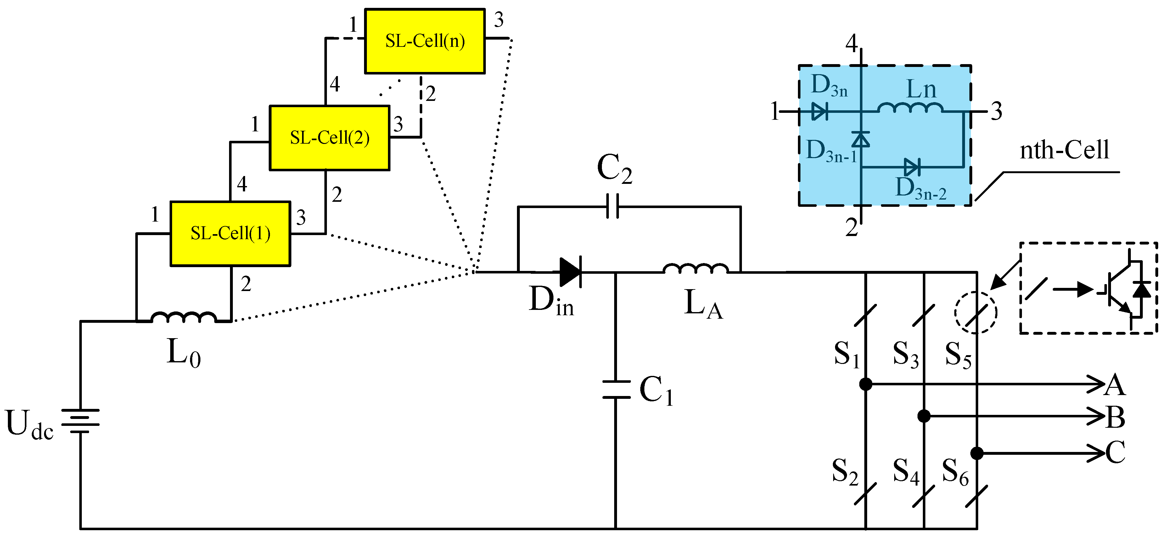
2. Traditional Multicell Switched-Inductor Quasi-Z-Source Inverter

The traditional multicell switched-inductor quasi-Z-source inverter topology (MSL-qZSI) [24] is shown in Figure 1, which is based on the qZSI, where the single inductor connected to the DC voltage source is replaced by an n-cell cascaded switched-inductor. Each of these switched-inductor cells is made up of three diodes and an inductor. As the number of n increases, the boost factor of the inverter rises gradually.
U P N = 1 + n D 1 2 D n D 2 U d c = B n U d c
Equation (1) is the voltage relationship equation for the MSL-qZSI topology, where n is the number of cascaded switched-inductor units, D is the duty cycle of the shoot-through state, and Bn is the boost factor of the inverter. The boost factor of the inverter increases as n increases.

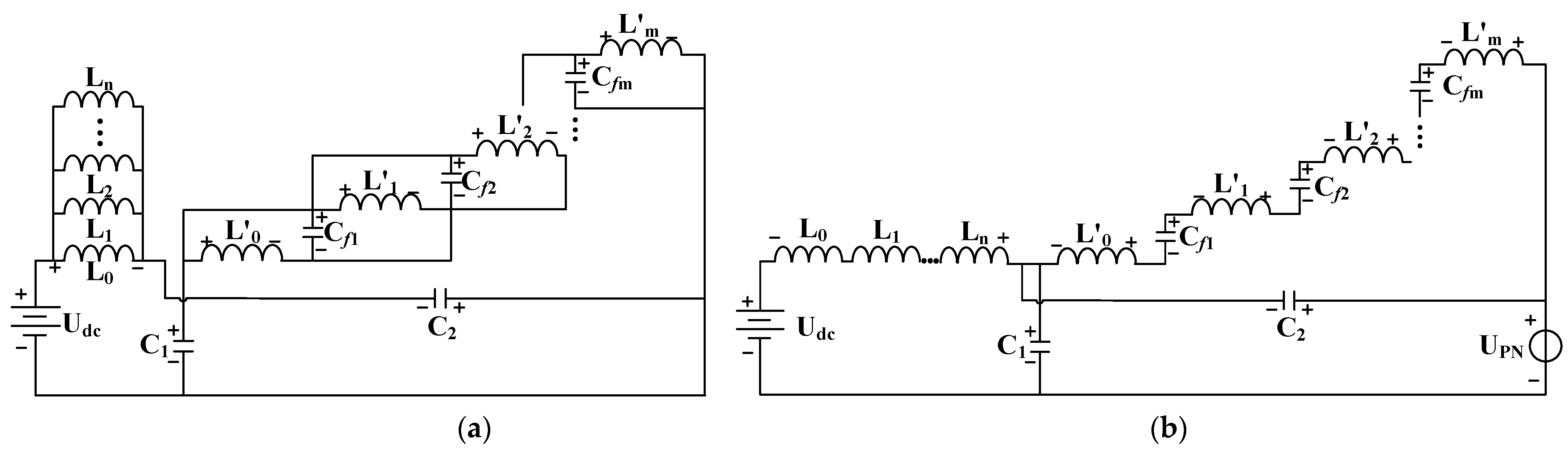
3. New Multicell Switched-Inductor Quasi-Z-Source Inverter

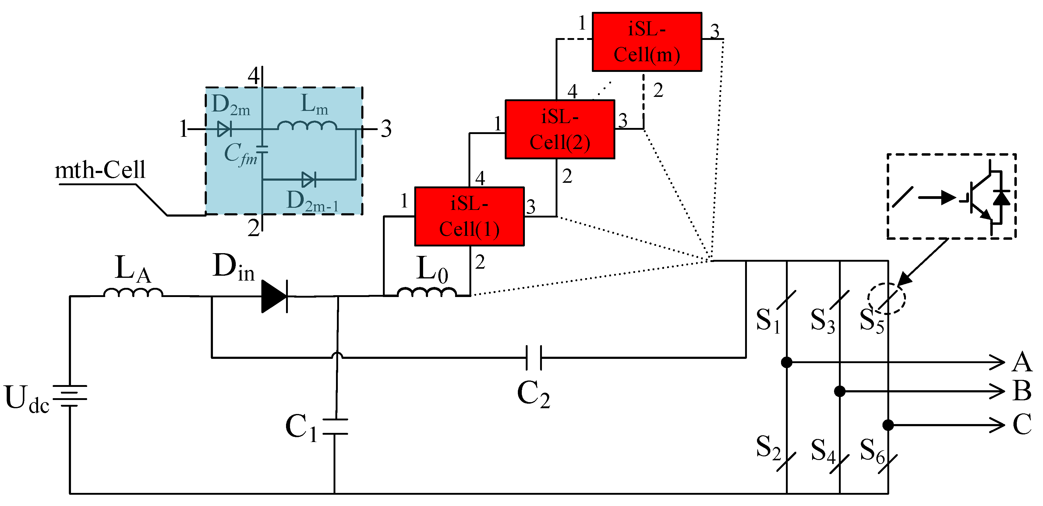
3.1. Multicell Improved-Switched-Inductor Quasi-Z-Source Inverter

The multicell improved-switched-inductor quasi-Z-source inverter (MISL-qZSI) topology proposed in this paper is based on the quasi-Z-source inverter, where the second inductor in the qZSI is replaced by a modified switched-inductor unit. The improved switched-inductor replaces a diode in the conventional switched-inductor unit with a capacitor, which has a higher boost capability. By cascading the modified switched-inductor cells, the MISL-qZSI topology can be obtained, as shown in Figure 2. For each modified switched-inductor unit, one inductor, one capacitor, and two diodes are required.
The MISL-qZSI topology has a shoot-through state and a non-shoot-through state, and the equivalent circuit is shown in Figure 3. For the convenience of analysis, let the inductance and capacitance in the impedance source network be equal, i.e., LA = L0 = … = Lm = L, Cf1 = Cf2 = … = Cfm = C1 = C2 = C.
In the shoot-through state, the three-phase inverter bridge can be replaced by a short line, with diodes D2m and D2m−1 on and diode Din off, whose equivalent circuit is shown in Figure 3a. In this case, capacitor C2 with a DC power supply together charges the inductor LA, capacitor C1, and Cf1, Cf2 … Cfm, and inductors L0, L1, L2 … Lm are connected in parallel. According to Kirchhoff’s voltage and current law and the characteristics of the components, the relationship of the circuit in the shoot-through state can be obtained:
U L A = U d c + U C 2 U C 1 = U L i = U C f j ( i = 0 , 1 m ; j = 1 m ) U P N = 0
In the non-shoot-through state, diode D2n and D2n−1 are off, while diode Din is on; its equivalent circuit diagram is shown in Figure 3b. Currently, capacitors Cf1, Cf2 … Cfm and inductors L0, L1, L2 … Lm are in series with C2 to constitute a circuit, and inductor LA and DC power supply together charge capacitor C1. At this time, according to the equivalent circuit diagram, the voltage relationship can be obtained as follows:
U L A = U C 1 U d c U C 2 = i = 0 m U L i + j = 1 m U C f j ( i = 0 , 1 m ; j = 1 m ) U P N = U C 1 + U C 2
From Equations (2) and (3), combined with volt-second equilibrium, we obtain:
D T ( U d c + U C 2 ) = ( 1 D ) T ( U C 1 U d c ) D T U C 1 = ( 1 D ) T U C 2 m U C f 1 m + 1
Since the voltage of the capacitor cannot change rapidly during a switching cycle, it can be assumed that the capacitor C1 is a voltage source, then according to Equation (2), it follows that:
U C 1 = U C f j ( j = 1 m ) .
From Equation (2) to Equation (5), the relationship between the capacitor voltage and the DC link voltage can be further derived as follows:
U C 1 = 1 D 1 ( m + 2 ) D U d c U C 2 = m + D 1 ( m + 2 ) D U d c U P N = 1 + m 1 ( m + 2 ) D U d c = B n U d c
where m is the number of cascades of the improved switched-inductor units, and B n is the boost factor of the inverter.

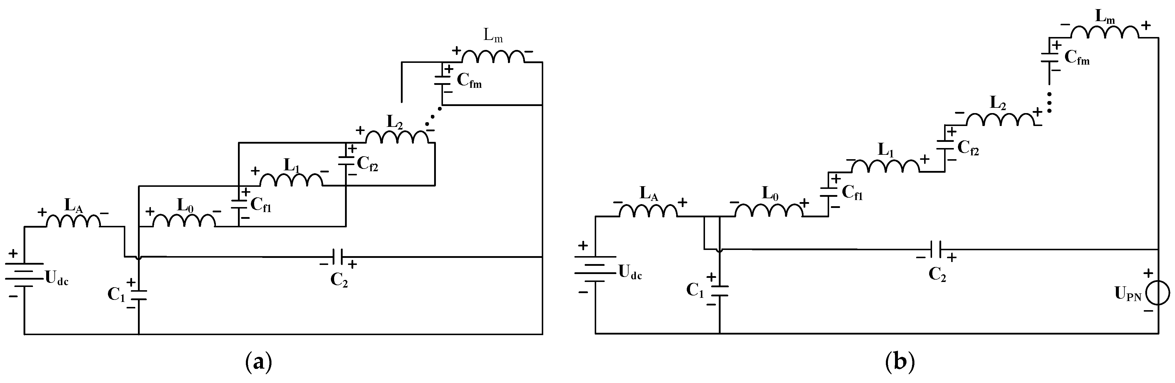
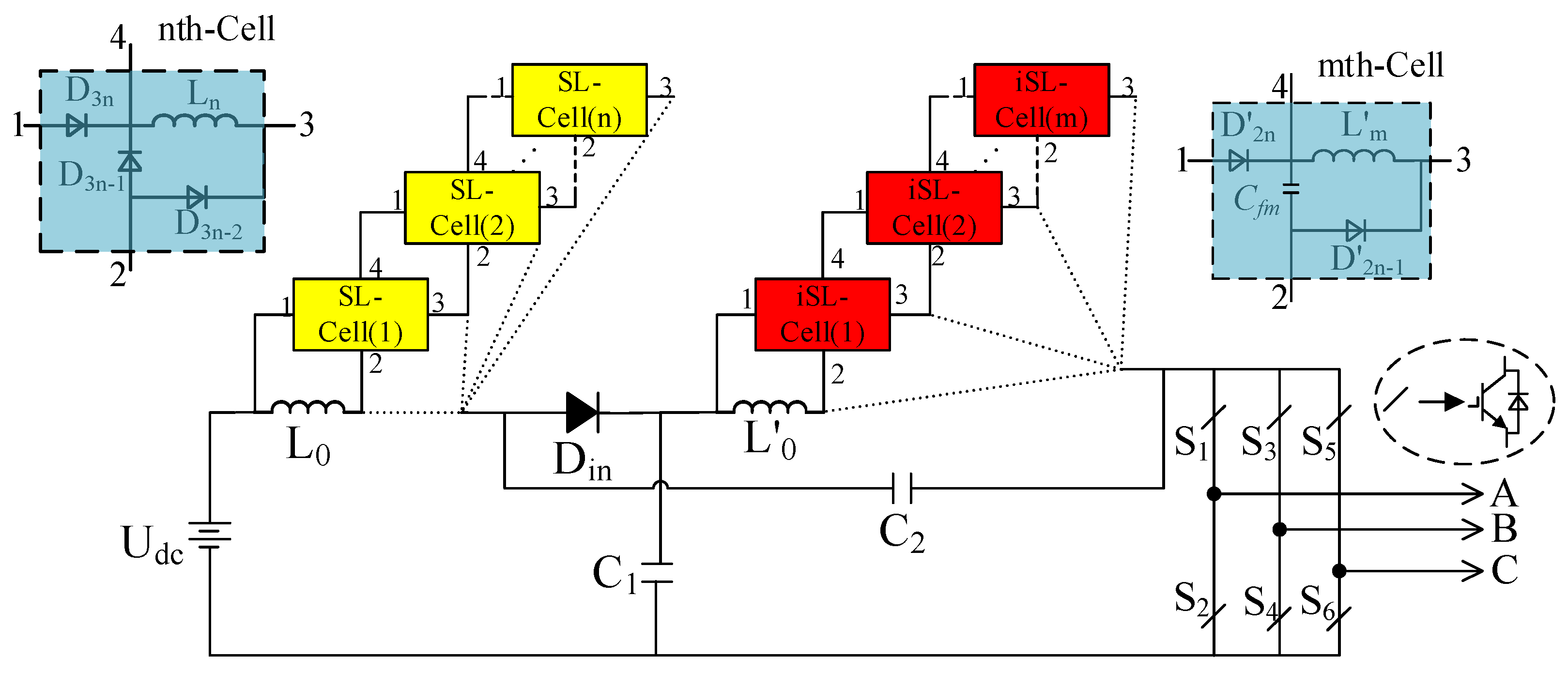
3.2. Hybrid Multicell Switched-Inductor Quasi-Z-Source Inverter

Combining the MSL-qZSI topology and the proposed MISL-qZSI, a hybrid multicell switched-inductor quasi-Z-source inverter (HMSL-qZSI) is obtained, as shown in Figure 4. This inverter replaces the first inductor in the quasi-Z source inverter with an n-cell cascaded switched-inductor, and the latter inductor with a m-cell modified switched-inductor. To simplify the analysis, let L0 = … =Ln =L′0 = … =L′m = L, Cf1 = Cf2 = … =Cfm = C1 = C2 = C.
In the shoot-through state, the diodes D3n and D3n−2 in the n-cell cascaded switched-inductor unit are in the forward conduction state, and the diode D3n−1 is in the reverse cutoff state. The diodes D2m and D2m−1 in the m-unit modified switched-inductor of the rear stage are on and the diode Din is off. At this time, capacitors C1, Cf1, Cf2 … Cfm and inductors L′0, L′1, L′2 … L′m are connected in parallel, and the DC power supply and capacitor C2 together charge the parallel inductors L0, L1, L2 … Ln. At this point, the following voltage relationship can be obtained:
U L 0 = U L 1 = = U L n = U d c + U C 2 U C 1 = U L i = U C f j ( i = 0 , 1 n ; j = 1 , 2 m ) U P N = 0
The equivalent circuit in the non-shoot-through state is shown in Figure 5b. Diodes D3n and D3n−2 in the n-cell switched-inductor unit reverse cutoff and diode D3n−1 conducts, while diodes D2n and D2n−1 in the m-unit modified switched-inductor in the rear stage reverse cutoff and diode Din conducts. Currently capacitors Cf1, Cf2 … Cfm and inductors L′0, L′1, L′2 … L′m in series charge capacitor C2, and inductors L0, L1, L2 … Ln in series with the DC power source supply capacitor C1. At this point, according to the equivalent circuit, the voltage relationship can be obtained as follows:
U C 1 U d c = k = 0 n U L k U P N = U C 1 + U C 2 U C 2 = i = 0 m U L i + j = 1 m U C f j
From Equations (7) and (8), and combined with the principle of volt-second equilibrium, the following relationship is derived:
D T ( U C 2 + U d c ) = ( 1 D ) T U C 1 U d c n + 1 D T U C 1 = ( 1 D ) T U C 2 m U c f m + 1 .
Furthermore, the following voltage relationship equation can be obtained:
U C 1 = ( 1 D ) ( 1 + n D ) 1 ( 2 + n m + m ) D n D 2 U d c U C 2 = ( m + D ) ( 1 + n D ) 1 ( 2 + n m + m ) D n D 2 U d c U P N = ( 1 + m ) ( 1 + n D ) 1 ( 2 + n m + m ) D n D 2 U d c = B n U d c .
From Equation (10), it can be noticed that when m and n are taken as different values, different types of topologies and boost factor relationships can be obtained. When m is 0, HMSL-qZSI topology is just the traditional multicell switched-inductor quasi-Z source inverter, and when n is 0, it is the MISL-qZSI topology.

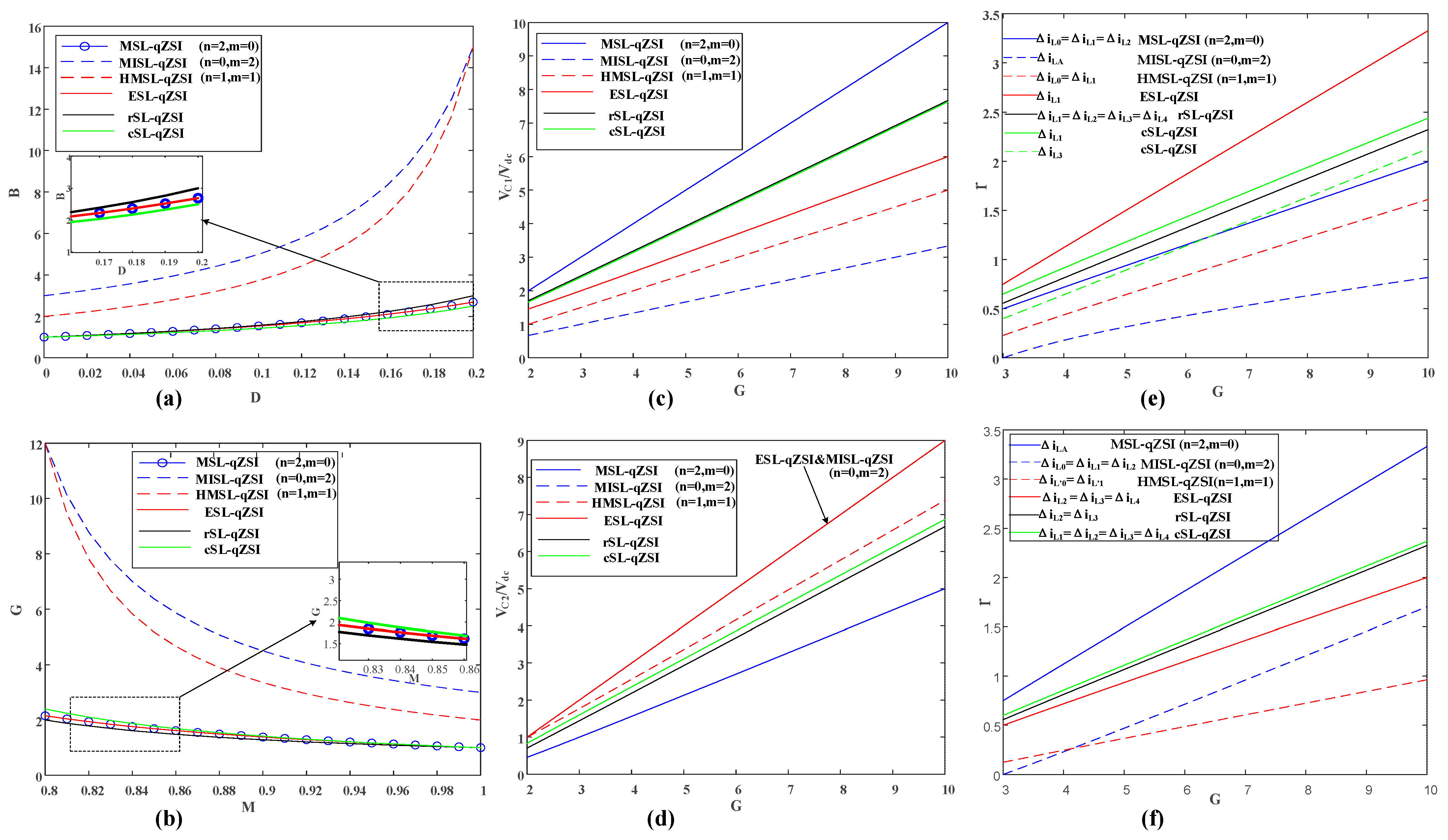
3.3. Comparative Analysis of the Boosting Capacity of Three Types of Inverters

In the previous sections, two new multicell switched-inductor quasi-Z-source inverter topologies were introduced and their operating principles and voltage relationship equations were investigated in detail. From Equations (1), (6) and (10), the boost factor of the inverter varies when the number of switched-inductor cells m, and n is taken to different values. Table 1 shows the boost factors for the three inverters when the total number of switched-inductor cells is 1, 2, 3, and 4.
Figure 6 shows the boost factor of the MSL-qZSI topology against the proposed MISL-qZSI topology and HMSL-qZSI topology for different numbers of switched-inductor units. For the same number of switched-inductor units, the boost factor of both MISL-qZSI and HMSL-qZSI is much larger than MSL-qZSI. Therefore, the proposed new inverter topology is more advantageous than the conventional topology in terms of boosting capability.

4. Comparative Analysis of the Performance of Inverters of the Same Type

In order to further demonstrate the superiority of the proposed new topology, an in-depth comparison is made with several existing Z-source inverters in terms of overall voltage gain, boosting capability, device stress, and current ripple. For brevity and to keep the number of components in the impedance source network comparable, the multicell topologies in this paper all use two switched-inductor cells, i.e., n = 2 for the MSL-qZSI topology, m = 2 for the MISL-qZSI topology and m = n = 1 for the HMSL-qZSI topology. Table 2 summarizes the number of components of the impedance source network in the inverters involved in the comparison. Each of the inverters in the comparison is obtained by adding the same number of switched-inductor units to the conventional Z-source inverter, and the number of components in the impedance source network remains the same. In Table 3, the expressions of important performance parameters of the proposed new topologies and each of the considered existing topologies are given.

4.1. Boosting Ability

Based on the boost factor of the different inverters in Table 3, Figure 7a shows the boost factors between the proposed new topologies in this paper and the existing topologies of the same type. It can be clearly seen that when the same shoot-through duty cycle D is taken, MISL-qZSI (n = 0, m = 2) has the largest boosting capability, followed by HMSL-qZSI (n = 1, m = 1). The performance advantage of the new topology in terms of boosting capacity is demonstrated.

4.2. Voltage Gain

From the literature [3], the voltage gain of a Z-source/quasi-Z-source inverter can be expressed as
G = M B = V o V d c / 2 ,
where Vo is the peak of the output phase voltage of the inverter, Vdc is the input DC voltage, M is the modulation index of the inverter, and B is the boost factor. The simple boost modulation strategy is all used in this paper, and the relationship between the modulation factor M and the shoot-through duty cycle D satisfies the following equation:
D = 1 M .
By substituting Equation (12) into the boost factor of different inverters, respectively, the relationship between G and M can be obtained as shown in Table 3. Figure 7b shows the comparison of the modulation index M versus the voltage gain G for these inverters. It can be clearly found that MISL-qZSI (n = 0, m = 2) and HMSL-qZSI (n = 1, m = 1) have a higher voltage gain G over the entire range of modulation index M compared to the existing inverters. Therefore, for the same overall voltage gain, the proposed topology can be operated with a higher modulation index M and a lower shoot-through duty cycle D, which means that the new inverter topology can obtain a higher quality output voltage.

4.3. Capacitor Voltage Stress

In addition to the boosting capacity, the voltage stress and current ripple of the components should also be of interest as indicators of the overall performance of the Z-source inverter. The magnitude of the voltage stress and current ripple directly determines the values of the capacitance and inductance in the impedance source network, which further affects the economic performance of the system. Therefore, it is necessary to analyze the capacitor voltage stress and inductor current ripple in different topologies.
Figure 7c,d shows the graphs of the voltage stresses of capacitors C1 and C2 with the inverter voltage gain in the above types of inverter topologies. From Figure 7c, it can be obtained that the voltage stress of capacitor C1 in the proposed MISL-qZSI topology is the smallest, followed by the HMSL-qZSI topology. The voltage stress of capacitor C2 in the HMSL-qZSI topology is significantly higher than the other topologies, while the voltage stress of C2 in the MISL-qZSI topology is in the intermediate range.

4.4. Inductor Current Ripple

Based on Table 3, the variation curves of the inductor current ripple pulsation coefficient r versus voltage gain G for different topologies are shown in Figure 7e,f. From Figure 7e,f, it can be found that the inductor current ripple of the proposed MISL-qZSI (n = 0, m = 2) and HMSL-qZSI (n = 1, m = 1) is smaller than that of the other topologies with the same voltage gain G.

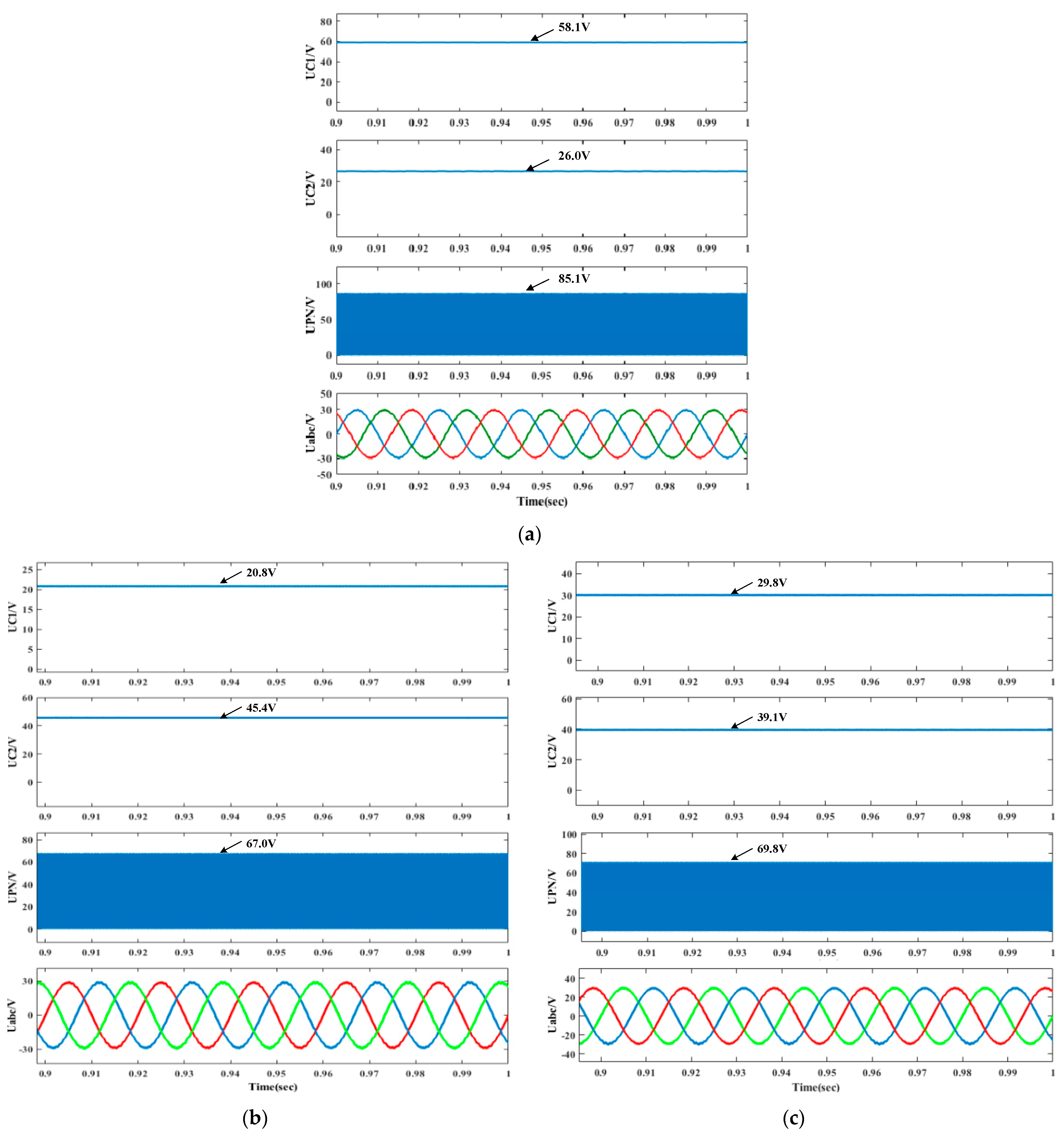
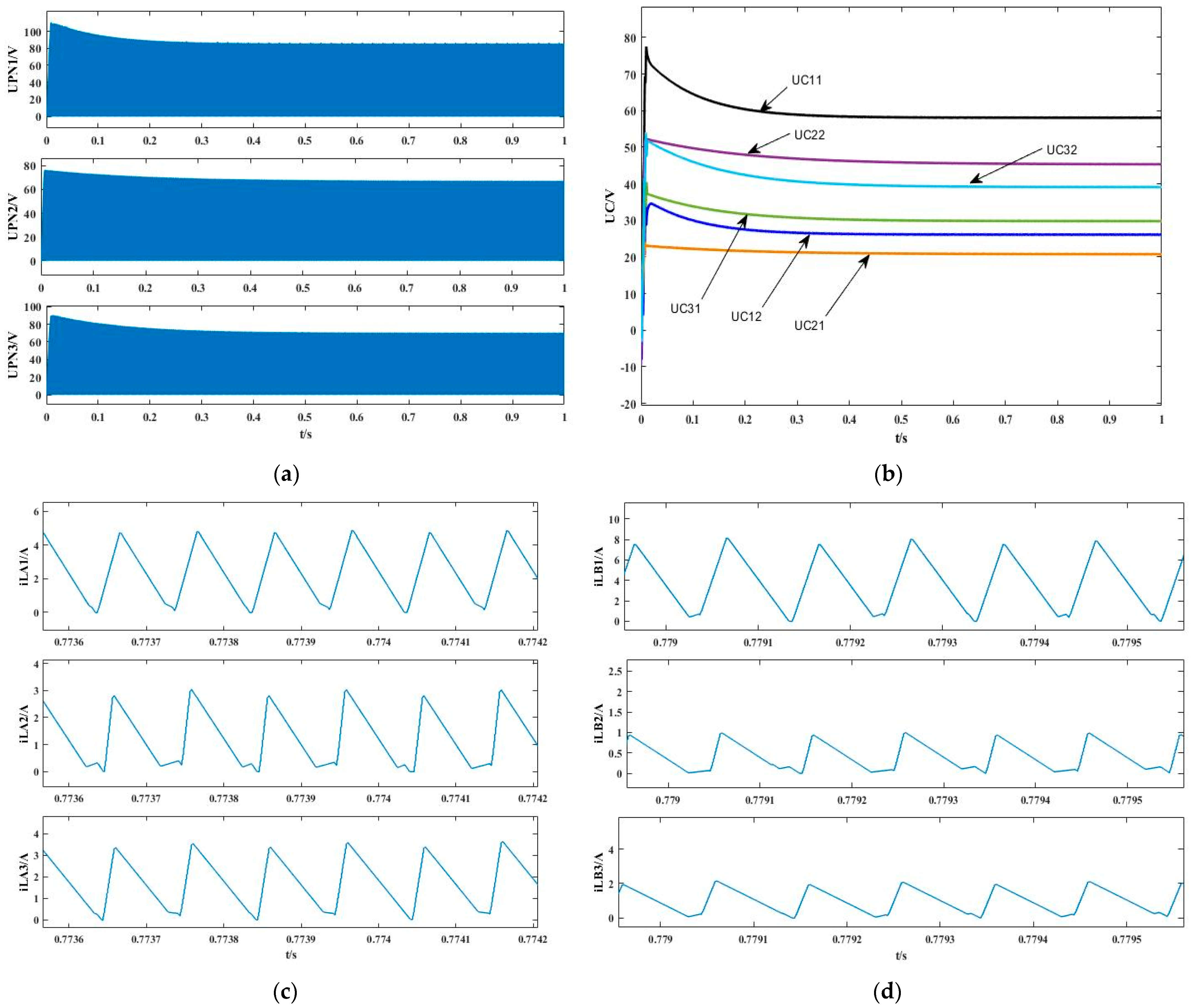
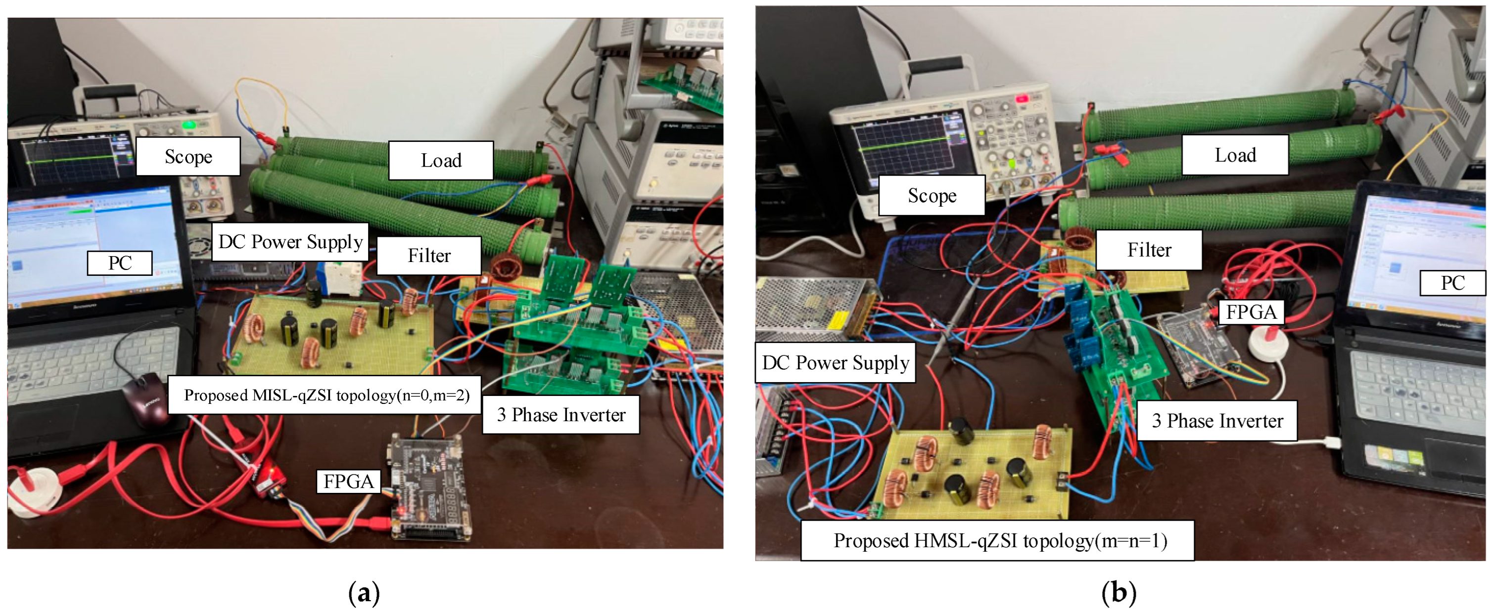
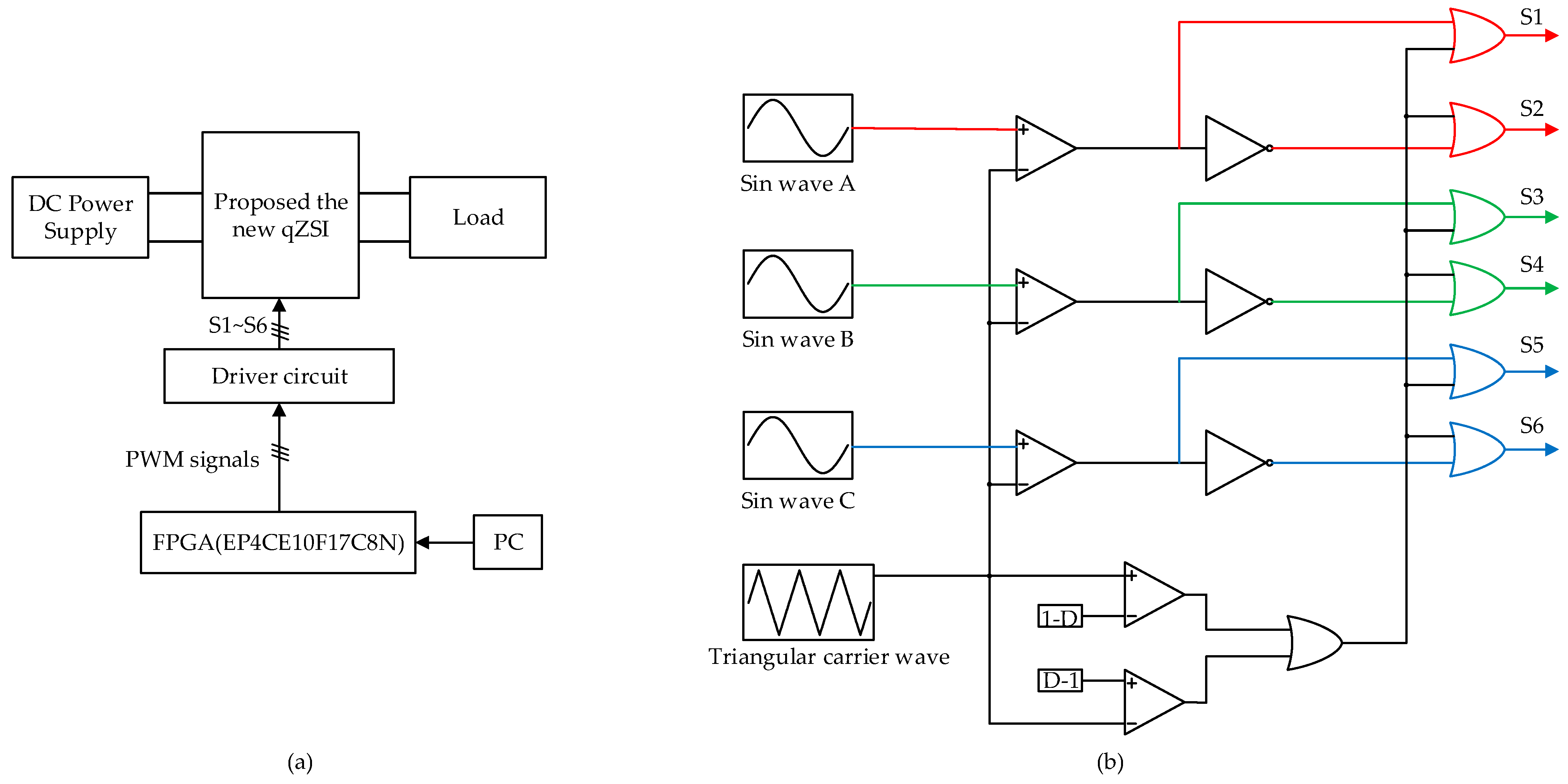
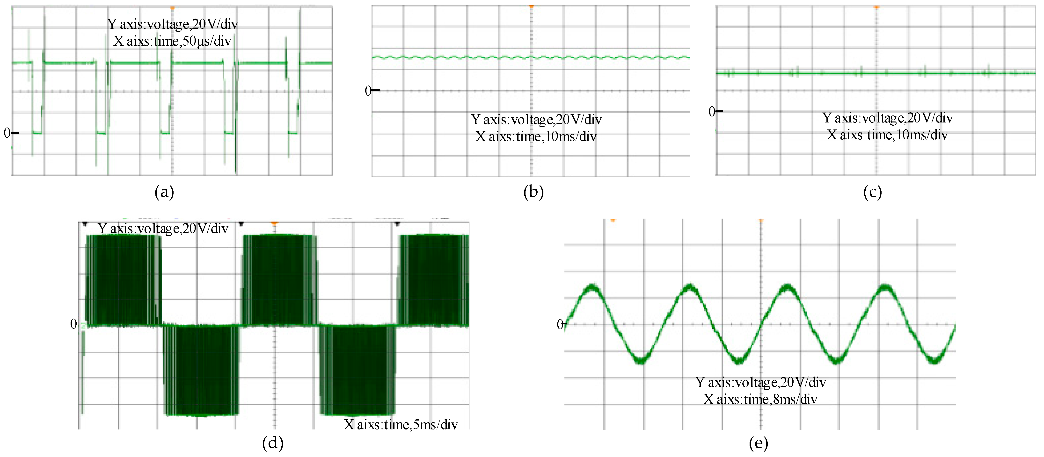
5. Simulation Analysis and Experimental Verification

In order to verify the superiority of the proposed topologies and the correctness of the previous theoretical analysis, the simulation models of MSL-qZSI topology (n = 2, m = 0), MISL-qZSI topology (n = 0, m = 2) and HMSL-qZSI topology (n = m = 1) are established in Matlab/Simulink. Then, small prototypes of MISL-qZSI (n = 0, m = 2) and HMSL-qZSI (n = m = 1) are further constructed for experimental verification.
As the simple boost modulation (SBM) is simple and effective, both the experimental and simulation parts will be conducted by SBM in this paper; the relevant parameters of the simulation and experiment are shown in Table 4. In order to compare the relevant performance of the inverter, the input voltage of each inverter is 12 V, and the peak value of the output phase voltage is 30 V. According to the input-output relationship of the inverter, the overall gain (G) of the inverter can be obtained as G = 5. From Equations (1), (6) and (10), the corresponding modulation index M and the shoot-through duty cycle D can be obtained as shown in Table 4, in which Mx and Dx (x = 0, 1, 2) correspond to the modulation index and the shoot-through duty cycle for the MSL-qZSI (n = 2, m = 0), MISL-qZSI (n = 0, m = 2), and HMSL-qZSI (n = m = 1), respectively.
Figure 8a–c shows the simulation waveforms of the three types of inverters with the same input voltage and the same output voltage, respectively. According to Equations (1), (6) and (10), the theoretical values are basically consistent with the simulation values.
From Figure 9a, it is known that when the overall gain of the inverters is the same, the DC chain voltage UPN is the lowest for the MISL-qZSI (n = 0, m = 2), followed by the HMSL-qZSI (n = m = 1). This result means that the voltage stress across the switches of the proposed new topology is smaller than that of the other topologies.
Figure 9b shows the simulation waveforms of the voltages of capacitors C1 and C2 in the three topologies. Among them, UC11, UC12, UC21, UC22, UC31, and UC32 are the voltage of capacitors C1 and C2 in the MSL-qZSI, MISL-qZSI, and HMSL-qZSI, respectively. For capacitor C1, the proposed MISL-qZSI and HMSL-qZSI topologies have lower voltage stress than the MSL-qZSI topology. Thus, the proposed new topology effectively lowers the voltage stress on capacitor C1 in the impedance source network.
The waveforms of the front- and back-stage inductor current of the impedance source network in the three inverters are shown in Figure 9c,d, respectively, where iLAx and iLBx (x = 1, 2, 3) correspond to the inductor current in the MSL-qZSI, MISL-qZSI (n = 0, m = 2), and HMSL-qZSI (n = m = 1) topologies, respectively. It is clear that the inductor current ripple in the proposed new topologies is smaller than the conventional type topologies.
To further verify the performance of the new topology, based on the theoretical and simulation analyses, small prototypes of MISL-qZSI (n = 0, m = 2) and HMSL-qZSI (n = m = 1) are built for experimental verification, and the experimental setups are shown in Figure 10a,b. The key parameters of the main circuit are shown in Table 4, which are the same as the simulation parameters. Based on the simple boost modulation, the gating signals of the three-phase inverter bridge are generated by ALTERA FPGA (EP4CE10F17C8N). The control block diagram of the experimental setup and the logic diagram of gate signal generation are shown in Figure 11.
Figure 12 and Figure 13 show the experimental results of the two types of inverters, respectively. The experimental results are slightly lower than the theoretical values due to the losses of passive components as well as switches in the impedance source network, but the errors are within the acceptable range, proving the correctness of the proposed topology.

6. Conclusions

Aiming at the problems of limited boost capability and high capacitor voltage stress in the traditional quasi-Z source inverter, a novel family of multicell switched-inductor quasi-Z source inverters is proposed in this paper. Simulation models and experimental platforms for MISL-qZSI (n = 0, m = 2) and HMSL-qZSI (n = m = 1) were constructed. Theoretical analyses, simulations, and experiments show that:
(1)
Compared to the conventional quasi-Z-source inverter, the proposed MISL-qZSI and HMSL-qZSI topology have higher boost capability, and its voltage stress across the capacitors and the current ripple through the inductors are effectively reduced.
(2)
As the number of cascaded switched-inductor units increases, the boost capability of the new inverter is significantly improved. Therefore, the designers can flexibly select the number of switched-inductor units in the new topologies to meet the requirements of practical applications.
The limitations of the research work in this paper include the following: (1) The selection of impedance source network parameters in the new inverter needs to be further optimized, and (2) the efficiency and cost-effectiveness of the new inverter have not been considered.
In the future, we will further analyze the efficiency, loss, and other properties of the new inverter and consider its application to photovoltaic power generation and motor drives.

Author Contributions

Conceptualization, J.T. and R.G.; methodology, J.T.; validation, J.T. and X.W.; writing—original draft preparation, J.T.; writing—review and editing, J.T., R.G. and H.W.; project administration, R.G.; funding acquisition, R.G. All authors have read and agreed to the published version of the manuscript.

Funding

This research was funded by the National Natural Science Foundation of China, grant number 61561007, and the Natural Science Foundation of Guangxi Province, China, grant number 2017GXNSFAA198168.

Data Availability Statement

The data used to support the findings of the study are available within the article.

Conflicts of Interest

The authors declare no conflict of interest.

References

  1. Tripathi, P.R.; Thakura, P.; Keshri, R.K.; Ghosh, S.; Guerrero, J.M. Twenty-Five Years of Single-Stage Buck–Boost Inverters: Development and Challenges. IEEE Ind. Electron. Mag. 2022, 16, 4–10. [Google Scholar] [CrossRef]
  2. Siwakoti, Y.P.; Peng, F.Z.; Blaabjerg, F.; Loh, P.C.; Town, G.E. Impedance-Source Networks for Electric Power Conversion Part I: A Topological Review. IEEE Trans. Power Electron. 2015, 30, 699–716. [Google Scholar] [CrossRef]
  3. Peng, F.Z. Z-Source Inverter. IEEE Trans. Ind. Appl. 2003, 39, 504–510. [Google Scholar] [CrossRef]
  4. Anderson, J.; Peng, F.Z. Four Quasi-Z-Source Inverters. In Proceedings of the 2008 IEEE Power Electronics Specialists Conference, Rhodes, Greece, 15–19 June 2008; pp. 2743–2749. [Google Scholar]
  5. Gajanayake, C.J.; Luo, F.L.; Gooi, H.B.; So, P.L.; Siow, L.K. Extended-Boost Z-Source Inverters. IEEE Trans. Power Electron. 2010, 25, 2642–2652. [Google Scholar] [CrossRef]
  6. Fathi, H.; Madadi, H. Enhanced-Boost Z-Source Inverters with Switched Z-Impedance. IEEE Trans. Ind. Electron. 2016, 63, 691–703. [Google Scholar] [CrossRef]
  7. Jagan, V.; Kotturu, J.; Das, S. Enhanced-Boost Quasi-Z-Source Inverters with Two-Switched Impedance Networks. IEEE Trans. Ind. Electron. 2017, 64, 6885–6897. [Google Scholar] [CrossRef]
  8. Zhu, M.; Yu, K.; Luo, F.L. Switched Inductor Z-Source Inverter. IEEE Trans. Power Electron. 2010, 25, 2150–2158. [Google Scholar]
  9. Nguyen, M.-K.; Lim, Y.-C.; Cho, G.-B. Switched-Inductor Quasi-Z-Source Inverter. IEEE Trans. Power Electron. 2011, 26, 3183–3191. [Google Scholar] [CrossRef]
  10. Deng, K.; Zheng, J.; Mei, J. Novel Switched-Inductor Quasi-Z-Source Inverter. J. Power Electron. 2014, 14, 11–21. [Google Scholar] [CrossRef]
  11. Lim, Y.-C.; Nguyen, M.-K.; Choi, J.-H. Two Switched-Inductor Quasi-Z-Source Inverters. IET Power Electron. 2012, 5, 1017–1025. [Google Scholar]
  12. Ho, A.-V.; Chun, T.-W.; Kim, H.-G. Extended Boost Active-Switched-Capacitor/Switched-Inductor Quasi-Z-Source Inverters. IEEE Trans. Power Electron. 2015, 30, 5681–5690. [Google Scholar] [CrossRef]
  13. Masoud, G.; Seyed Masoud, B.; Bin, W. Extended Switched-Inductor Quasi-Z-Source Inverter: Modeling and Prototype Realization. Int. Trans. Electr. Energy Syst. 2019, 29, e2744. [Google Scholar]
  14. Abbasi Bolaghi, J.; Taheri, A.; Babaei, M.H.; Gholami, M. Quasi Z-Source Inverter with Switched-Capacitor-Inductor for Enhancing Boost Factor. IET Power Electron. 2021, 14, 2545–2562. [Google Scholar] [CrossRef]
  15. Qian, W.; Peng, F.Z.; Cha, H. Trans-Z-Source Inverters. IEEE Trans. Power Electron. 2011, 26, 3453–3463. [Google Scholar] [CrossRef]
  16. Loh, P.C.; Li, D.; Blaabjerg, F. Γ-Z-Source Inverters. IEEE Trans. Power Electron. 2013, 28, 4880–4884. [Google Scholar] [CrossRef]
  17. Siwakoti, Y.P.; Loh, P.C.; Blaabjerg, F.; Town, G.E. Y-Source Impedance Network. IEEE Trans. Power Electron. 2014, 29, 3250–3254. [Google Scholar] [CrossRef]
  18. Tang, Y.; Sun, H.; Wang, S. A Family of High Step-Up Quasi Z-Source Inverters with Coupled Inductor. Energies 2020, 13, 5667. [Google Scholar] [CrossRef]
  19. Sharifi, S.; Chulaee, Y.; Zarchi, H.A.; Monfared, M. Generalized Three-Winding Switched-Coupled-Inductor Impedance Networks with Highly Flexible Gain. IEEE Trans. Ind. Electron. 2021, 68, 2130–2141. [Google Scholar] [CrossRef]
  20. Ji, Y.; Geng, L.; Li, F.; Liu, H.; Wheeler, P. An Enhanced-Boost Coupled-Inductor Impedance Network Inverter Without Limitation of Inductor Parameters. IEEE Trans. Transp. Electrif. 2022, 8, 699–709. [Google Scholar] [CrossRef]
  21. Tang, Y.; Wang, T.; Fu, D. Multicell Switched-Inductor/Switched-Capacitor Combined Active-Network Converters. IEEE Trans. Power Electron. 2015, 30, 2063–2072. [Google Scholar] [CrossRef]
  22. Li, D.; Loh, P.C.; Zhu, M.; Gao, F.; Blaabjerg, F. Generalized Multicell Switched-Inductor and Switched-Capacitor Z-Source Inverters. IEEE Trans. Power Electron. 2013, 28, 837–848. [Google Scholar] [CrossRef]
  23. Majeed, R.; Chughtai, A.H. Multicell Schemes for Active-Switched-Capacitor and Active-Switched-Capacitor/Switched- Inductor Quasi-Z-Source Inverters. IEEE J. Emerg. Sel. Top. Power Electron. 2020, 8, 1739–1754. [Google Scholar] [CrossRef]
  24. Cheng, Z.; Cheng, J.; Yu, H.; Ye, S.; Zhang, Z. Switched-inductor quasi-Z -source inverter based on multi-cascaded. J. Anhui Univ. Nat. Sci. 2013, 37, 48–56. [Google Scholar]
  25. Barath, J.N.; Soundarrajan, A.; Stepenko, S.; Husev, O.; Vinnikov, D.; Nguyen, M.-K. Topological Review of Quasi-Switched Boost Inverters. Electronics 2021, 10, 1485. [Google Scholar] [CrossRef]
Figure 1. Traditional multicell switched-inductor quasi-Z source inverter topology.
Electronics 12 03814 g001
Figure 2. MISL-qZSI topology.
Electronics 12 03814 g002
Figure 3. Equivalent circuit diagram: (a) shoot-through state; (b) non-shoot-through state.
Electronics 12 03814 g003
Figure 4. HMSL-qZSI topology.
Electronics 12 03814 g004
Figure 5. Equivalent circuit: (a) shoot-through state; (b) non-shoot-through state.
Electronics 12 03814 g005
Figure 6. (a) Boost factor comparison between MSL-qZSI and MISL-qZSI; (b) boost factor comparison between MSL-qZSI and HMSL-qZSI.
Electronics 12 03814 g006
Figure 7. The Comparison of MISL-qZSI (n = 0, m = 2) and HMSL-qZSI (n = 1, m = 1) with other topologies; (a) the boost factor; (b) the overall voltage gain; (c) the voltage stress of capacitor C1; (d) the voltage stress of capacitor C2; (e) the current stress of inductor LA; (f) the current stress of inductor LB.
Electronics 12 03814 g007
Figure 8. Simulation waveforms of the three types of inverters. From top to bottom, the waveforms are the capacitor voltage UC1, the capacitor voltage UC2, the peak dc-link voltage UPN, and the three-phase output phase voltage Uabc. (a) MSL-qZSI (n = 2, m = 0); (b) MISL-qZSI (n = 0, m = 2); (c) HMSL-qZSI (n = m = 1).
Electronics 12 03814 g008
Figure 9. Comparison of simulation results for three inverters: (a) the peak dc-link voltage UPN; (b) the capacitor voltage UC; (c) the inductor current iLA; (d) the inductor current iLB.
Electronics 12 03814 g009
Figure 10. Photograph of the experimental setup: (a) MISL-qZSI (n = 0, m = 2); (b) HMSL-qZSI (n = m = 1).
Electronics 12 03814 g010
Figure 11. (a) block diagram of the experimental setup; (b) logic diagram of gate signal generation.
Electronics 12 03814 g011
Figure 12. Experimental results for MISL-qZSI (n = 0, m = 2): (a) the dc-link voltage UPN; (b) the capacitor voltage UC1; (c) the capacitor voltage UC2; (d) the unfiltered output line voltage Uab; (e) the filtered output phase voltage Ua.
Electronics 12 03814 g012
Figure 13. Experimental results for HMSL-qZSI (n = m = 1): (a) the dc-link voltage UPN; (b) the capacitor voltage UC1; (c) the capacitor voltage UC2; (d) the unfiltered output line voltage Uab; (e) the filtered output phase voltage Ua.
Electronics 12 03814 g013
Table 1. Boost factor for different numbers of switched-inductor cells.
Topology TypeMSL-qZSI (m = 0)MISL-qZSI (n = 0)HMSL-qZSI (m, n ≠ 0)
Num of
SL Units
1 1 + D 1 2 D D 2 2 1 3 D /
2 1 + 2 D 1 2 D 2 D 2 3 1 4 D 2 ( 1 + D ) 1 4 D D 2
3 1 + 3 D 1 2 D 3 D 2 4 1 5 D 3 ( 1 + D ) 1 6 D D 2 (m = 2, n = 1)
2 ( 1 + 2 D ) 1 5 D 2 D 2 (m = 1, n = 2)
4 1 + 4 D 1 2 D 4 D 2 5 1 6 D 3 ( 1 + 2 D ) 1 8 D 2 D 2 (m = 2, n = 2)
Table 2. Comparative analysis of passive component count.
ParametersMSL-qZSI
(n = 2, m = 0)
MISL-qZSI (n = 0, m = 2)HMSL-qZSI (n = 1, m = 1)ESL-qZSI [10]rSL-qZSI [11]cSL-qZSI [11]
Number of L444444
Number of C243222
Number of D756777
Total131313131313
Table 3. Expressions of important performance parameters in each considered topology.
ParametersBGDVCΔI
MSL-qZSI
(n = 2, m = 0)
1 + 2 D 1 2 D 2 D 2 M ( 3 2 M ) 3 + 6 M 2 M 2 2 G + 1 A 4 4 G V C 1 V d c = G V C 2 V d c = G ( 2 G + 1 A ) 3 6 G + A Δ I L 0 = Δ I L 1 = Δ I L 2 = G ( 2 G + 1 A ) 6 2 A T V d c L Δ I L A = G ( 2 G + 1 A ) 4 4 G T V d c L
MISL-qZSI (n = 0, m = 2) 3 1 4 D 3 M 4 M 3 G 3 4 G 3 V C 1 V d c = V C 3 V d c = G 3 V C 2 V d c = G 1 Δ I L A = ( G 3 ) ( G + 3 ) 3 ( 4 G 3 ) T V d c L Δ I L 0 = Δ I L 1 = Δ I L 2 = ( G 3 ) ( G 1 ) 4 G 3 T V d c L
HMSL-qZSI (n = 1, m = 1) 2 ( 1 + D ) 1 4 D D 2 2 M ( 2 M ) 4 + 6 M M 2 4 G X 4 2 G V C 1 V d c = G 2 V C 2 V d c = G ( 4 + 2 G X ) 2 ( 4 6 G + X ) Δ I L 0 = Δ I L 1 = G ( 4 G X ) 2 G X + 4 T V d c L Δ I L 0 = Δ I L 1 = G ( 4 G X ) 2 ( 4 2 G ) T V d c L
Esl-qZSI [7] 1 + 2 D 1 2 D 2 D 2 M ( 3 2 M ) 3 + 6 M 2 M 2 2 G + 1 A 4 4 G V C 1 V d c = G ( 2 2 G ) 3 A V C 2 V d c = 3 G ( 2 2 G ) ( 2 G + 1 A ) ( 3 A ) ( 3 6 G + A ) Δ I L 1 = G ( 2 G + 1 A ) 4 4 G T V d c L Δ I L 2 = Δ I L 3 = Δ I L 4 = G ( 2 G + 1 A ) 6 2 A T V d c L
rsl-qZSI [11] 1 + D 1 3 D M 3 M 2 3 G Y 2 V C 1 V d c = 2 3 G + Y 2 9 G + 3 Y V C 2 V d c = 6 G 2 Y 2 9 G + 3 Y Δ I L 1 = Δ I L 2 = Δ I L 3 = Δ I L 4 = G ( 3 G Y ) 2 + 3 G Y T V d c L
csl-qZSI [11] 1 1 3 D M ( 2 M ) 3 M 2 G 1 3 G 1 V C 1 V d c = G ( 3 G 1 ) 4 G 2 V C 2 V d c = ( G 1 ) ( 3 G 1 ) ( 4 G 2 ) Δ I L 1 = ( G 1 ) ( 3 G 2 1 ) ( 4 G 2 ) ( 3 G 1 ) T V d c L Δ I L 2 = Δ I L 4 = G ( G 1 ) 4 G 2 T V d c L Δ I L 3 = ( G 1 ) 2 4 G 2 T V d c L
Notes: A = 12 G 2 12 G + 9 ; X = 20 G 2 16 G + 16 ; Y = 9 G 2 4 G + 4 .
Table 4. Simulation and experiment parameters.
ParameterValueParameterValue
DC voltage sources Udc/V12Modulation index M00.70127
Carrier frequency fc/kHZ5Shoot-through duty ratio D00.29873
Output frequency f0/HZ50Modulation index M10.88235
Inductors L/μH220Shoot-through duty ratio D10.11765
Capacitors C/μF1000Modulation index M20.85323
Filter inductors Lf/mH1Shoot-through duty ratio D20.14677
Filter capacitors Cf/μF20Overall voltage gain G = M × B5
Disclaimer/Publisher’s Note: The statements, opinions and data contained in all publications are solely those of the individual author(s) and contributor(s) and not of MDPI and/or the editor(s). MDPI and/or the editor(s) disclaim responsibility for any injury to people or property resulting from any ideas, methods, instructions or products referred to in the content.

