Article

Design, Implementation, and Characterization of a Compact Lock-in Add-on for Low-Frequency Impedance Measurements

by
Sara Pettinato
1,
Armando Piccardi
2,
Maria Cristina Rossi
3 and
Stefano Salvatori
1,*
1
Engineering Faculty, Niccolò Cusano University, Via don Carlo Gnocchi 3, 00166 Rome, Italy
2
Computer Engineering Faculty, Giustino Fortunato University, Via Raffaele Delcogliano 12, 82100 Benevento, Italy
3
Department of Industrial, Electronic, and Mechanical Engineering, Università degli Studi Roma Tre, Via Vito Volterra 62, 00146 Rome, Italy
*
Author to whom correspondence should be addressed.
Electronics 2023, 12(16), 3406; https://doi.org/10.3390/electronics12163406
Submission received: 15 July 2023 / Revised: 29 July 2023 / Accepted: 9 August 2023 / Published: 10 August 2023

Abstract

:
Impedance measurements are crucial in a variety of applications, from the characterization of lithium batteries, microbial fuel cells, and biosensors to the study of polymers and material degradation, where strict requirements have to be met in terms of frequency bandwidth and current level. Here, we present a cost-effective compact solution for ultra-low-frequency impedance measurements, operating in a wide range, from 1 mHz to 250 kHz. Coupled to a lock-in amplifier, the designed circuit is based on a Howland current pump cascaded by a precision current divider in order to set the conversion factor at 100 nA/V, 1 μA/V, or 100 μA/V. Therefore, it is possible to generate very low-current signals to measure resistive impedances up to 100 MΩ. In addition, a feedback network is inserted to null the voltage drift induced by leakage currents and offset voltages, thus allowing the measurement of low-capacitance loads, experimentally tested down to 10 nF. Remarkably, the feedback network allows to perform measurements also in the presence of high voltage bias of the load and experimental results performed up to 60 V demonstrate the excellent stability of the designed system, thus a high voltage compliance. The proposed circuit is particularly interesting for the conditioning of both resistive and capacitive sensors and it is likely to be an effective solution for the implementation of a portable instrument for measuring signals from biosensors.

Graphical Abstract

1. Introduction

Electrochemical impedance spectroscopy (EIS) is a non-invasive measurement technique employed for the characterization of complex systems [1]. It is widely used in several research fields and various applications such as corrosion monitoring [2], characterizations of solar cells [3], food control [4], and biomedical applications [5,6,7,8].
In some specific applications, very tight constraints must be met in terms of current levels and frequency bandwidth. Indeed, several examples of impedance measurements in a very low frequency range are shown in the literature. In [9], the Warburg impedance of Li-ion cells in the range 0.1 mHz–100 Hz is investigated. Ultra-low-frequency impedance spectroscopy is also used for the investigation of wood [10], in the range 1 mHz–100 Hz, and for the analysis of thermoelectric modules [11] in the range 1 mHz–10 kHz. Impedance measurements down to 0.01 Hz are also useful for studying the deterioration of Mg electrodes [12], for characterizing microbial cell fuels [13,14], for studying the capacitive properties of polymers [15], for bioimpedance measurements [16] and for the characterization of biosensors [17].
High-performance impedance meters operating over a wide range of frequencies are commercially available [18,19]. Several low-cost solutions have been reported in the literature. Most of them are based on the AD5933 impedance converter from Analog Devices managed by a microcontroller. However, the proposed solutions reach down to a few tens [20,21] or hundreds [22] of Hz, thus not allowing impedance analysis at ultra-low frequencies. Piasecki et al. [23] describe an ultra-low frequency (down to 1 mHz) impedance meter based on the STM32F405RG microcontroller (STMicroelectronics) that uses the embedded DAC and ADC both to generate the excitation signal and to acquire the load signal. Recently, a low-cost, portable impedance analyzer, down to a few mHz, which exploits a commercial soundboard coupled to tailored external hardware and open software to adapt the configuration to the specific application has been proposed [24].
When weak signals are employed, the lock-in amplifier (LIA) appears to be the most adequate solution for voltage-signal acquisitions, guaranteeing a very high dynamic reserve, up to more than 100 dB. LIAs are used in several application areas, including EIS techniques and lock-in-based impedance analyzers have been also proposed [25,26].
The LIA input stage is optimized for voltage signal acquisitions with very high full input dynamics (from about 1 nV to more than 1 V) in a wide frequency range (from 1 mHz to about 100 kHz). LIAs allow impedance measurements implementing the amperometric measurement method, i.e., injecting a sinusoidal current IZ in the device under test (DUT) and acquiring the voltage signal VZ at DUT ends. A two-phase LIA, which receives the reference signal at the same frequency and phase of IZ, recovers both the amplitude and the phase shift of VZ, allowing for the calculation of the complex impedance by the ratio between VZ and IZ. Importantly, LIAs implement a high-performance sinusoidal oscillator, which can be used as an internal reference signal VREF, as well as be replicated at the output. An LIA can be effective for precision impedance measurements implementing a versatile and high-accuracy voltage-to-current (V/I) converter, which takes VREF as input and produces the DUT current IZ. The Howland current pump configuration is a popular solution for delivering precise current signals, also applied for ultra-low frequency EIS [27].
In this work, an add-on analog circuit for a commercial, portable USB lock-in amplifier is proposed for impedance measurements in the wide frequency range 1 mHz–250 kHz. The LIA is used both to generate the excitation signal and to acquire the voltage signal generated at the ends of the system under analysis. A Howland circuit based on the high-precision LT1995 gain-selectable amplifier operates as a V/I converter (100 µA/V), taking the sinusoidal reference signal of the LIA and thus injecting a known current in the DUT. A precision current divider, based on an LT1996, has also been inserted in order to lower the V/I conversion factor down to 1 µA/V or 100 nA/V, hence increasing the versatility of the system and allowing high impedance measurements. In addition, the prototypal circuit implements a feedback network assuring good performance also for capacitive loads and complex RC networks, as well as for biased DUTs (i.e., guaranteeing high voltage compliance, tested up to 60 V). The benefits of the proposed prototype are high compactness, versatility, and cost-effectiveness.

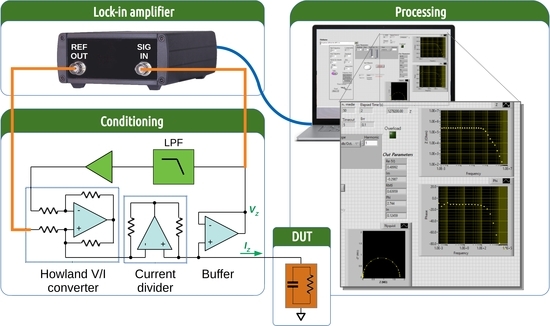
2. Materials and Methods

The solution proposed in this work is a lock-in add-on for impedance measurements of RC loads. In particular, a portable USB lock-in amplifier (Anfatec mod. 250) was used for the experimental characterization. The LIA was used to source an excitation signal VS (generated by the LIA internal oscillator), which is converted to the current IZ injected in the DUT using a custom-made voltage-to-current converter based on the Howland circuit. Then, with respect to the reference voltage VS, the LIA acquires both the modulus and the phase shift of the voltage VZ at the DUT ends as a function of the signal frequency. The DUT impedance is then calculated as the modulus and the phase-shift components of the VZ/IZ ratio. Table 1 outlines the main features of the Anfatec LIA used in this work. Although the manufacturer declares a minimum nominal frequency of 10 mHz, the instrument was adequate down to 1 mHz, as shown by the experimental results illustrated below.
The acquisitions of the complex components of VZ were performed with a specifically developed Labview virtual instrument (VI). From the front panel of the VI, the user sets the measurement parameters (e.g., both the amplitude and the frequency range of the sinusoidal signal generated by the LIA internal oscillator), and the Bode diagrams are displayed during data-sample recording. We set up the measurements to acquire up to 50 samples for each component at each frequency, then calculated the mean value and the standard deviation of each sample, obtaining a maximum error ~1%. For a rough evaluation of measurement repeatability, each DUT characterization has been repeated five times, observing an error within 1–3%.

3. Description and Characterizations of the Prototypes

The solution proposed in this paper is intended to feature extremely low-frequency operation (1 mHz) and a low V/I conversion coefficient as well, allowing for precise impedance measurements in specific applications. In addition, it must be insensitive to leakage currents for the measurement of capacitive loads, guaranteeing stability and reliability, and ensuring, at the same time, a high degree of portability and cost effectiveness. All these properties have been met using high-precision commercial devices, acting on their configuration to obtain suitable functionalities. A detailed description of the system implemented in this work is reported in the following subsections.

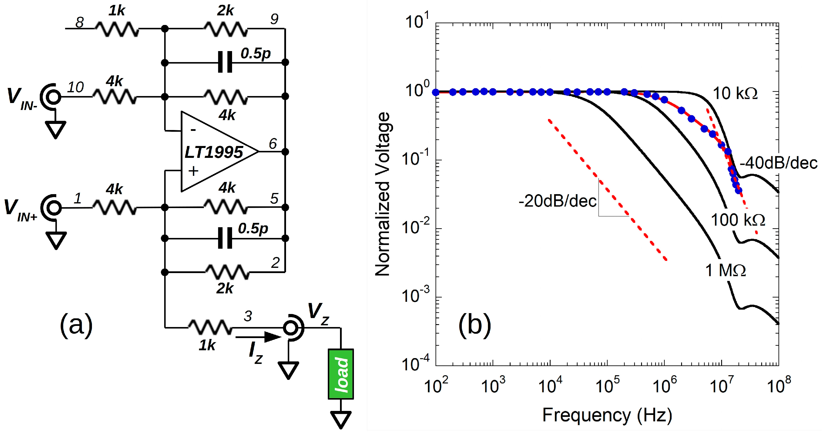
3.1. Basic Voltage-to-Current Converter Using the Conventional Howland Current Pump

To perform an efficient V/I conversion, a first stage employing an LT1995 IC from Analog Devices with suitable band characteristics was configured to obtain a Howland current pump. The most important feature of the selectable-gain amplifier LT199x series is the integration of excellent matched resistors, well suited for the implementation of a good balanced resistor bridge in the Howland circuit [28]. As sketched in Figure 1a, at the op-amp inputs, this chip is equipped with three couples of matched thin-film resistors (pins 1–3, 8–10). The net of resistors has been connected to achieve the desired balanced-bridge condition with the two feedback resistors (pins 5 and 6). The excellent resistor matching (0.2%) and the very low temperature coefficient (−30 ppm/°C) featured by the integrated thin-film resistors ensure an ideal environment to obtain a stable and highly accurate bridge condition for the Howland bridge circuit.
The V/I conversion is performed by connecting the load to one of the unused resistors (pin 3). This represents the main drawback of using a selectable-gain amplifier topology for the implementation of the Howland circuit for sourcing an RLOAD load. Indeed, the output voltage dynamics are limited, owing to the lack of a direct connection between the load and the non-inverting terminal of the op-amp. Such a limitation has been minimized using the lowest resistance (V/I output series resistance ROUT = 1 kΩ), thus reducing the unwanted voltage drop at its ends. For the typical Howland circuit (load directly connected to the op-amp non-inverting input [29]), the voltage V(+) at the non-inverting input is equal to IZ·RLOAD, where IZ is the load current. Conversely, for the circuit of Figure 1, V′(+) = (RLOAD + ROUT)·IZ. Hence, the loss in dynamics, calculated as [V(+) − V′(+)]/V(+), is ROUT/RLOAD. This implies that, when connected to a 10 kΩ resistive load, the circuit can provide 10% less than the ideal maximum output voltage, while for RLOAD >> 1 kΩ, the output dynamic limitation can be neglected.
Figure 1b shows the behavior of the LT1995 Howland circuit as simulated in the wide 102–108 Hz frequency range by LTSPICE software (continuous lines) for different values of the resistive load. By simulations, the position of the dominant-pole shifts from 5 MHz down to about 100 kHz as the load value increases from 10 kΩ to 1 MΩ. The typical bandwidth of LIAs is 100–250 kHz. Therefore, simulations shown in Figure 1b confirm the effectiveness of the proposed V/I converter coupled to an LIA for low-frequency impedance characterizations.
It is worth noting that the simulation carried out for 1 MΩ clearly shows a response with the dominant pole positioned at about 50 kHz, i.e., the presence of an equivalent parasitic capacitance Ceq~3 pF in parallel to the load, coherent with the LT1995 capacitance of 2.5 pF (typical) of each input pins declared for the device [30]. Moreover, in the Howland circuit, the finite gain bandwidth product (GBW) of the op-amp mainly affects the output capacitance COUT seen between the op-amp inverting input and ground [31]. For the LT1995, GBW~30 MHz and COUT~7 pF is estimated for the configuration shown in Figure 1a.
The circuit sketched in Figure 1a was then assembled for fast prototyping on a copper board using Manhattan style construction and enclosed in an aluminum box where three BNC connectors were used for VIN+, VIN−, and VZ connections. The integrated circuit was supplied at ±15 V and two 100 nF decoupling capacitors have been soldered close to the supply pins of the chip (not shown in the figure).
The circuit was preliminarily characterized by means of a digital oscilloscope (Agilent, DSO-X 3024A) connected at the output VZ with a 1 m coaxial cable. An Agilent 33220A waveform generator was used as the sinusoidal voltage source at the VIN+ input. To reduce the insertion loss, the waveform generator was set for 50 Ω termination. Therefore, to assure the balanced-bridge condition for the Howland circuit, the VIN− input was terminated with 50 Ω. Measurements have been carried out with a 10 kΩ load from 100 Hz to 20 MHz. Dots in Figure 1b are the ratio between the rms values of VIN+ and VZ as acquired by the oscilloscope, then normalized to the maximum value recorded at the lowest frequency. As it can be observed, the simulations reproduce the experimental measurements well for the 10 kΩ resistor for both the frequency values up to hundreds of kHz and the slope of −40 dB/decade at higher frequency. The discrepancy between the simulated and the experimental behavior in the range 0.5–10 MHz is tentatively attributed to the parasitic capacitance of the coaxial cable used for VZ connection. For a parasitic capacitance of about 100 pF (typical of 1 m coaxial cables [32]), a 200 kHz cut-off frequency is found and consistent to the result shown in Figure 1b. Significantly, such a result underlines the requirement of decoupling the load voltage VZ for accurate impedance measurements, i.e., mitigating the effect of parasitic components in parallel to the load. A solution in this regard is described in the next subsection where an upgraded version of the V/I converter is shown.

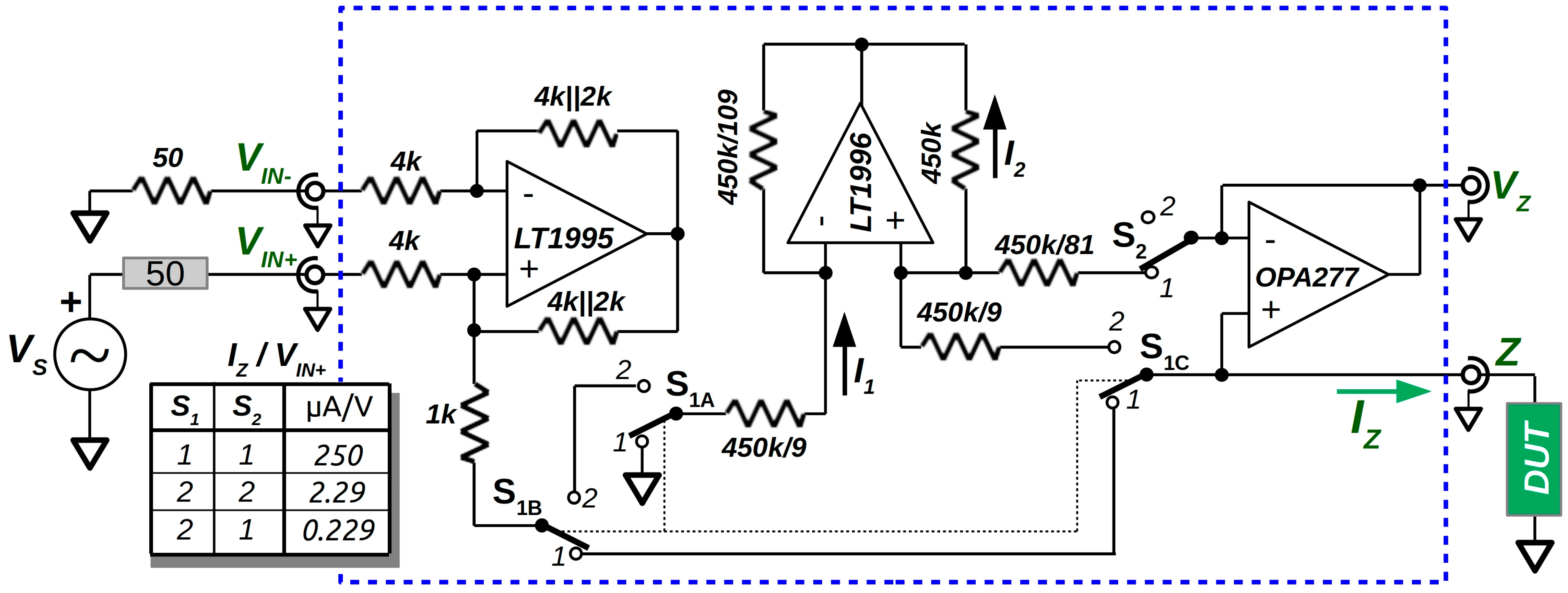
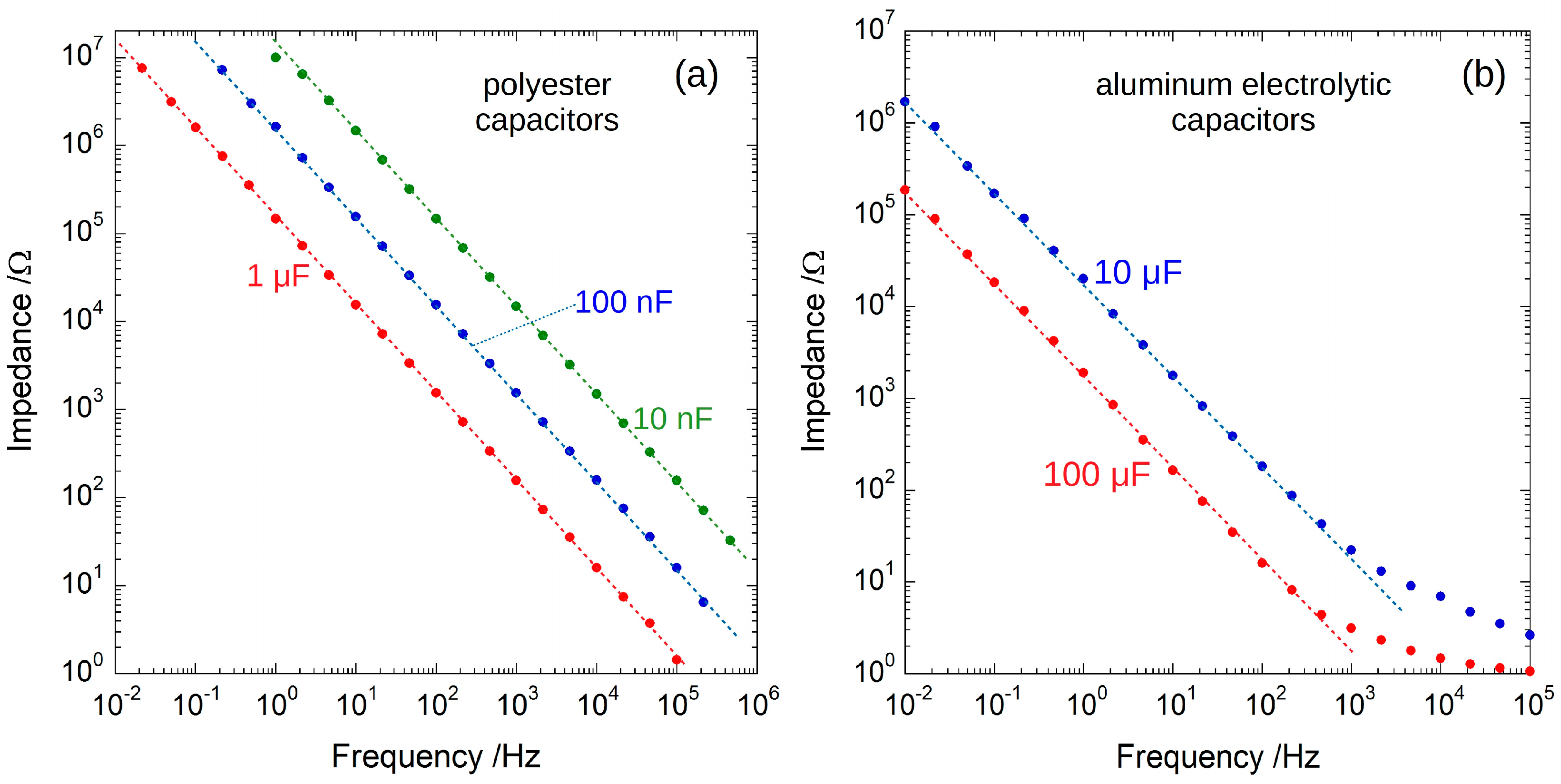
3.2. The Voltage-to-Current Converter for Low-Level Currents

In the basic configuration of Figure 1a, the voltage-to-current conversion coefficient results in IZ/VIN+ = 1/R1, where R1 is the resistance connected to the input signal. The choice of R1 (pin1, 4 kΩ) ensures the minimum available conversion coefficient for the LT1995-based Howland circuit, nominally 250 µA/V.
To further decrease the conversion coefficient down to extremely low values, a different configuration has been implemented. Figure 2 sketches the schematic of the proposed circuit, where only the relevant components are shown, using two switches (S1 and S2) allowing for setting different values for the conversion coefficient. For S1A–C switches in the ‘1′ position, the circuit is almost equivalent to the previously described configuration, except for the presence of the output buffer based on an OPA277 for decoupling the load voltage to the acquisition system.
When S1A-C are switched to ‘2’, a further stage is employed in the IZ output current path. A second IC has been used, namely the LT1996 high-precision selectable-gain amplifier equipped with high-value internal resistors and configured to act as a current divider [33,34]. Like in the first stage, the high quality of thin-film resistors ensures a precise and stable ratio between resistances in the input and output branches, which defines an exact current division I2/I1 = 1/109 (see Figure 2). The load connected to one of the resistors still reduces the output voltage dynamics. (In the next subsection, it will be shown how the final design overcomes the limit of the output voltage dynamics.) Nonetheless, it is worth noting the advantage of the implemented circuit in decreasing the V/I coefficient with the current division by more than two orders of magnitude, i.e., down to 2.29 µA/V.
The voltage buffer placed as the output stage provides two main roles. The first is to further divide the current flowing in the DUT: when the S1C and S2 switches connect the op-amp inputs to the current divider outputs (S1C = 2 and S2 = 1, see Figure 2), the buffer also acts to reduce the load current, further attenuating IZ by a factor of 10. Therefore, the conversion coefficient is reduced to 229 nA/V. At the same time, as mentioned, the buffer allows for decoupled-load voltage acquisition.
The circuit was assembled and enclosed in a metal box with BNC connectors and supplied at ±15 V. We evaluated the main feature of the assembled circuit by using a set of resistors as loads. To reduce the electromagnetic interference and the induced noise, especially for very-high values of load resistance, each resistor was encapsulated in a small copper box and connected to the Z input with a short (10 cm) coaxial cable. For the measurements, the circuit was coupled to the Anfatek LIA (mod. 250). The sinusoidal VIN+ signal was generated by the LIA (50 Ω terminated) internal oscillator, whereas VZ was connected to the input of the instrument. As indicated in Figure 2, the VIN− input was terminated at 50 Ω as well, to guarantee the balanced-bridge condition of the Howland circuit.
To obtain insight on system performances, the proposed circuit has been tested in the 1 mHz–1 MHz frequency range for different resistive load values in the range 100 Ω–100 MΩ. Figure 3 shows the Bode diagrams of the acquired data. The amplitude (Figure 3a) and the phase shift (Figure 3b) plots follow a single-pole behavior with a −20 dB/decade slope at high frequency. As expected, the lower the load value, the higher the cut-off frequency. In the 100 kΩ–100 MΩ range, a parasitic capacitance COUT~40 pF in parallel to the load is evaluated by the frequency position of the −3 dB attenuation and the −45° phase shift in Bode diagrams of Figure 3. In this case, measurements were performed with the current divider (switch S1 = 2 in Figure 2). Then, the cut-off frequency is mainly attributed to the output capacitance of the current divider. Indeed, a GBW < 1 MHz is declared for the LT1996 [35], thus an output capacitance COUT of a few tens of pF is estimated [31]. On the other hand, for resistances from 100 Ω to 10 kΩ, only the LT1995-based Howland pump was used to have a higher conversion coefficient. In this range, the attenuation observed for f > 105 Hz is attributed to the bandwidth limit of the LIA (250 kHz).

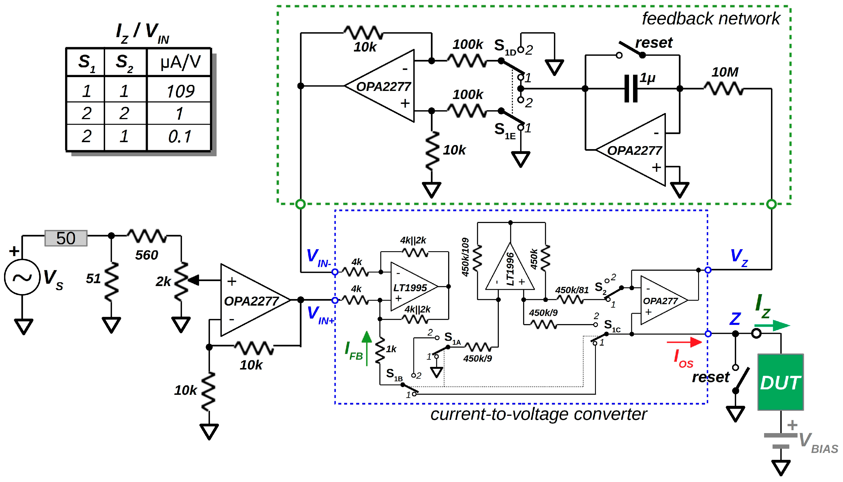
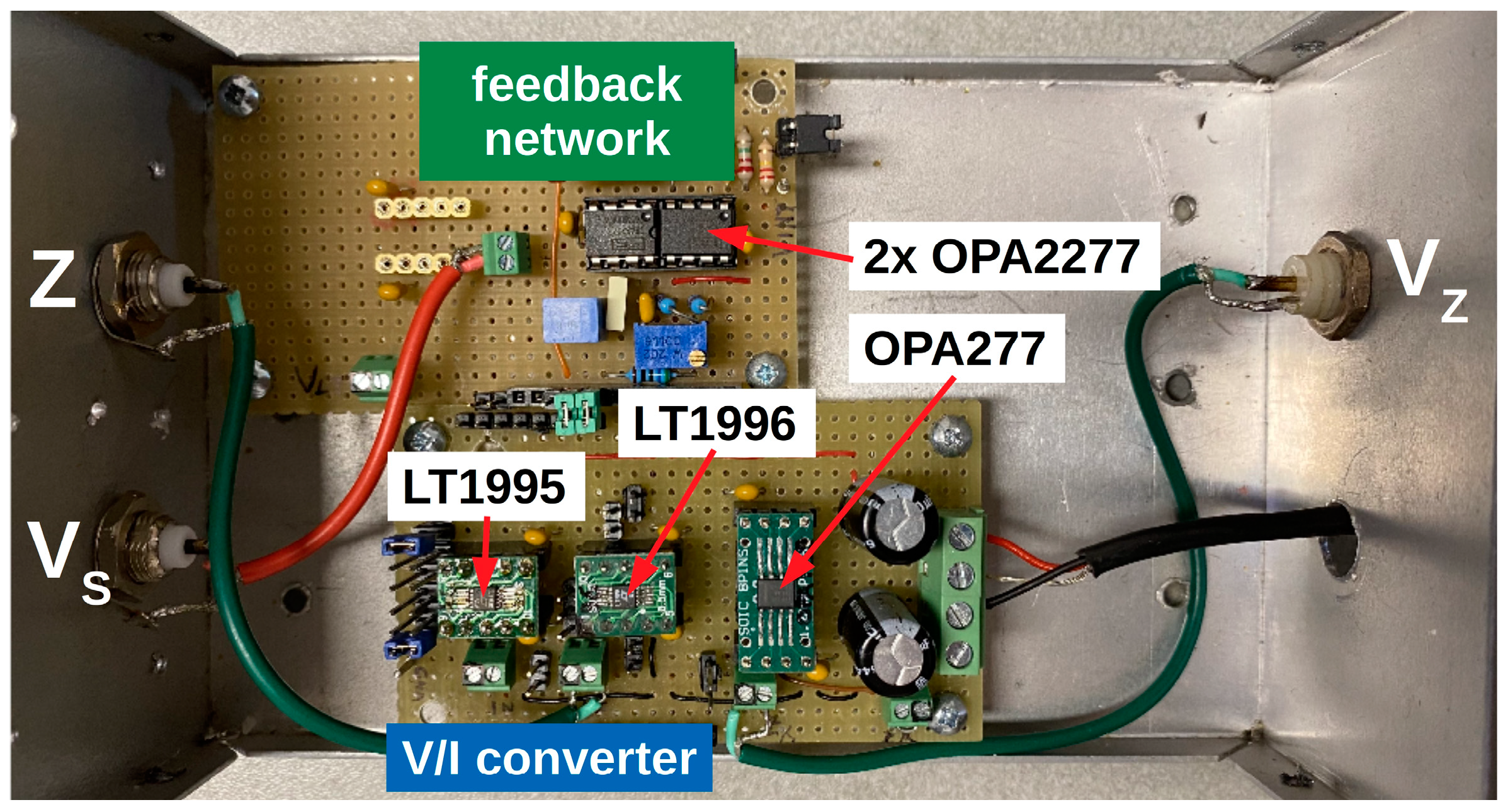
3.3. A V/I Converter with High Output Voltage Compliance

The main drawback of the solution illustrated in Figure 2 is that any offset current of both the Howland current pump and the op-amp current divider generates a leakage current in the DUT. For pure resistive loads, this results in an offset voltage that sums up to that of the OPA277 buffer. The LIA is able to eliminate any constant contribution within its input dynamics (5 V for the Anfatec 250), thus amplifying only the AC component of interest. However, for purely capacitive loads, leakage currents generate a drift of the VZ output voltage for the circuit reported in Figure 2. As an example, Figure 4 shows the signal VZ recorded by the digital oscilloscope during the characterization of a 1 µF capacitor (VS = 5 V, 30 Hz, and V/I coefficient 2.29 µA/V). Importantly, the drift of the output voltage VZ can reach the limits of the lock-in input dynamics, therefore saturating its input stage.
A simple solution to overcome the aforementioned drawback is to discharge the load capacitor through a MOSFET switch whenever the voltage gets close to the LIA limit as detected by a comparator driving the gate of the MOSFET. However, for such an implementation, the MOSFET capacitance affects the overall measured impedance, reducing the measurement accuracy. Conversely, to adapt the circuitry of Figure 2 to capacitive-load measurements and attenuate the DC component of the VZ signal, we added an analog feedback network to the circuit of Figure 2, as shown in Figure 5.
An integrator produces an output voltage proportional to the average value of VZ. The following stage drives the inverting input VIN− of the Howland current pump, which produces a constant current counteracting the DC current flowing into the DUT, i.e., the DC component of VZ. When considering the presence of a DC offset current IOS at the V/I output (S1 switch connected as indicated in Figure 5, i.e., current divider not selected), we have to take into account that OPAx227 op-amps offer an ultra-low offset voltage VOS (±10 μV at room temperature, ±100 μV in the range −40 °C–+85 °C), and ±2.8 nA maximum bias current IB. On the contrary, LT1995 and LT1996 show 5 mV and 0.2 mV maximum VOS, and typical 0.6 μA and 2.5 nA for IB, respectively. Therefore, the IOS value of about 2.5 μA is evaluated as dominated by both the VOS and IB of the LT1995 chip.
Let us assume IOS is sourcing the Z output, as indicated in Figure 5. When both the reset switches are closed, they discharge the feedback capacitor and the DUT, and force the voltage VZ to zero as well. During the reset period, IOS flows to ground and the integrator output voltage is equal to the op-amp offset voltage (±10 μV typical). On the other hand, when the reset switches are opened, the IOS flows in the DUT inducing an increase in VZ. Therefore, the output voltage of the integrator decreases and its amplitude is reported as an increase in VIN− by the inverting amplifier implemented in the feedback network. Then, the Howland current pump injects an IFB current flowing, as shown by the green arrow in Figure 5, i.e., counteracting the IOS and closing the negative feedback path of the system. The steady state condition is reached when IFB ≅ IOS, thus keeping to a stable value the VZ voltage. When the current divider is selected (S1 = 2), the negative feedback is still guaranteed by implementing a non-inverting amplifier in the network (see S1D and S1E in position “2”).
However, when the period of the sinusoidal signal VS is comparable to the integrator response time, the feedback network also induces an attenuated component at the same frequency of VS, thus affecting the V/I conversion factor in both the amplitude and the phase. To address this drawback, the values of the components implemented in the feedback network were chosen to provide the best trade-off between the integrator response time and the measurement accuracy at low frequencies. The feedback network, in the final assembly, provides an integration time of 10 s and an attenuation of 10 for the second stage. It is worth to note that the steady state value of VZ was of the order of a few tens of mV for all DUTs characterized in this work.
The circuit shown in Figure 5 also includes a 50 Ω adapter at VIN+ based on a non-inverting op-amp stage, where the trimmer was adjusted to set the V/I conversion factors reported in the table of the same figure. Significantly, the inaccuracy was maintained well below 1% for frequencies down to 2 mHz. As indicated in the schematic of Figure 5, the non-inverting input stage and the amplifier of the feedback network are based on a single OPA2277 chip. The same solution can be used for the buffer at the converter output and the integrator, thus increasing only by one the number of chips used in comparison to the open-chain solution of Figure 2.
Figure 6 shows the picture of the assembled prototype. Two different boards were used to assemble the V/I converter and the feedback network circuits. The latter includes an OPA2277 to implement the input 50 Ω adapter.
Figure 7 shows the results obtained with the completed prototype for the 1 μF capacitor, highlighting the effectiveness of the feedback network in mitigating the drift of the signal observed for the open-chain V/I converter (Figure 4).
Figure 8 reports the experimental results obtained for a set of polyester and aluminum electrolytic capacitors. As expected, for polyester capacitors (Figure 8a), the impedance is inversely proportional to the signal frequency up to the ~250 kHz limit of the lock-in amplifier. Conversely, for electrolytic capacitors (Figure 8b), the effect of an equivalent series resistance of a few Ohms is found at high frequency.
Very remarkably, the adopted solution also allows the characterization of DUTs when using a bias voltage. Indeed, let us assume that we insert a continuous voltage source VBIAS in series to the load (as indicated in light color in Figure 5). Before the measurement session, with both the reset switches closed, VBIAS is applied at the DUT ends, whereas VZ is fixed at virtual ground. Then, when the reset switches are open, the series between the DUT and the VBIAS is connected between Z and ground. In this condition, the feedback network starts reacting to maintain the VZ voltage around 0 V, driving the current pump via the VIN− input to supply the DC current required by the load.
Figure 9a shows the characterization of an aluminum electrolytic capacitor (1 μF, 16 V) carried out at different VBIAS. The device shows the same behavior up to the working voltage declared by the manufacturer. However, a different behavior is observed for twice the maximum allowed voltage: the capacitance decreases, whereas the equivalent series resistance increases, as expected for aged capacitors [36,37]. This result highlights the effectiveness of the designed system to monitor the state of capacitors, especially when employed in switching-power-supply applications.
Figure 9b shows the behavior observed for a tantalum capacitor (1 μF, 50 V). In this case, the device did not show any significant performance degradation at 60 V for 5 h.
Finally, the prototype was also tested measuring the impedance of a complex RC network that emulates the response of a diamond biosensor [17], see Figure 10a. The impedance of the emulated sensor was measured between 0.1 Hz and 100 kHz. Figure 10b reports the Bode diagrams for both the experimental results and the LTSPICE circuit simulation of the RC network. The experimental results are in excellent agreement with simulations, corroborating the data reported in the literature as well. These results confirm that the proposed circuit is suitable for impedance measurements in the wide frequency range required for the characterization of this class of diamond biosensors.

4. Conclusions

This work describes a lock-in add-on for ultra-low-frequency impedance measurements from 250 kHz down to 1 mHz. The solution is based on a Howland circuit operating as a V/I converter. Thanks to a high-precision current divider, conversion factors of 100 nA/V, 1 μA/V, and 100 μA/V can be selected. We designed, assembled and characterized a prototype which has been tested on resistive loads, allowing precise measurements from 100 Ω to 100 MΩ. A tailored feedback system has been designed to eliminate the voltage drift on capacitors induced by leakage currents. The adopted solution allows for the measurement of the complex impedance on several kinds of capacitors in the 10 nF–100 µF range, also demonstrating a high voltage compliance, at least up to 60 V, as verified by experiments. In addition, we tested the possibility to analyze the equivalent impedance of a biosensor, forecasting applications in setups where strict constraints have to be met in terms of frequency and current level. The good technical features of the device combine with compactness, cost-effectiveness and portability.

Author Contributions

Conceptualization, S.S. and S.P.; methodology, S.S.; software, S.P.; validation, S.S., S.P. and A.P.; formal analysis, S.S.; investigation, S.S. and S.P.; resources, S.S. and M.C.R.; data curation, S.S. and S.P.; writing—original draft preparation, S.P. and A.P.; writing—review and editing, S.S. and M.C.R.; visualization, A.P. and M.C.R.; supervision, S.S. All authors have read and agreed to the published version of the manuscript.

Funding

This research received no external funding.

Data Availability Statement

Data sharing is not applicable to this article.

Conflicts of Interest

The authors declare no conflict of interest.

References

  1. Bonanos, N.; Steele, B.C.H.; Butler, E.P. Applications of Impedance Spectroscopy. In Impedance Spectroscopy: Theory, Experiment and Applications, 2nd ed.; Barsoukov, E., Macdonald, J.R., Eds.; John Wiley & Sons, Inc.: Hoboken, NJ, USA, 2005; pp. 205–520. [Google Scholar]
  2. Zhu, H.; Luo, H.; Ai, D.; Wang, C. Mechanical impedance-based technique for steel structural corrosion damage detection. Measurement 2016, 88, 353–359. [Google Scholar] [CrossRef]
  3. Fabregat-Santiago, F.; Garcia-Belmonte, G.; Mora-Seró, I.; Bisquert, J. Characterization of nanostructured hybrid and organic solar cells by impedance spectroscopy. Phys. Chem. Chem. Phys. 2011, 13, 9083–9118. [Google Scholar] [CrossRef]
  4. Grossi, M.; Riccò, B. Electrical impedance spectroscopy (EIS) for biological analysis and food characterization: A review. J. Sens. Sens. Syst. 2017, 6, 303–325. [Google Scholar] [CrossRef] [Green Version]
  5. Carrion, B.; Wells, A.; Mayhew, J.; Koch, A. Concordance among Bioelectrical Impedance Analysis Measures of Percent Body Fat in Athletic Young Adults. Int. J. Exerc. Sci. 2019, 12, 324–331. [Google Scholar]
  6. Yao, J.; Wang, L.; Liu, K.; Wu, H.; Wang, H.; Huang, J.; Li, J. Evaluation of electrical characteristics of biological tissue with electrical impedance spectroscopy. Electrophoresis 2020, 41, 1425–1432. [Google Scholar] [CrossRef] [PubMed]
  7. Schwarzenberger, T.; Wolf, P.; Brischwein, M.; Kleinhans, R.; Demmel, F.; Lechner, A.; Becker, B.; Wolf, B. Impedance sensor technology for cell-based assays in the framework of a high-content screening system. Physiol. Meas. 2011, 32, 977. [Google Scholar] [CrossRef]
  8. Stupin, D.D.; Kuzina, E.A.; Abelit, A.A.; Emelyanov, A.K.; Nikolaev, D.M.; Ryazantsev, M.N.; Koniakhin, S.V.; Dubina, M.V. Bioimpedance spectroscopy: Basics and applications. ACS Biomater. Sci. Eng. 2021, 7, 1962–1986. [Google Scholar] [CrossRef] [PubMed]
  9. Oldenburger, M.; Beduerftig, B.; Gruhle, A.; Grimsmann, F.; Richter, E.; Findeisen, R.; Hintennach, A. Investigation of the low frequency Warburg impedance of Li-ion cells by frequency domain measurements. J. Energy Storage 2019, 21, 272–280. [Google Scholar] [CrossRef]
  10. Martin, T.; Nordsiek, S.; Weller, A. Low-frequency impedance spectroscopy of wood. J. Res. Spectrosc. 2015, 1, 1–9. [Google Scholar]
  11. García-Cañadas, J.; Min, G. Low frequency impedance spectroscopy analysis of thermoelectric modules. J. Electron. Mat. 2014, 43, 2411–2414. [Google Scholar] [CrossRef] [Green Version]
  12. Gomes, M.P.; Costa, I.; Pébère, N.; Rossi, J.L.; Tribollet, B.; Vivier, V. On the corrosion mechanism of Mg investigated by electrochemical impedance spectroscopy. Electrochim. Acta 2019, 306, 61–70. [Google Scholar] [CrossRef] [Green Version]
  13. Ramasamy, R.P.; Gadhamshetty, V.; Nadeau, L.J.; Johnson, G.R. Impedance spectroscopy as a tool for non-intrusive detection of extracellular mediators in microbial fuel cells. Biotechnol. Bioeng. 2009, 104, 882–891. [Google Scholar] [CrossRef]
  14. Sekar, N.; Ramasamy, R.P. Electrochemical impedance spectroscopy for microbial fuel cell characterization. J. Microb. Biochem. Technol. 2013, 6, 1–14. [Google Scholar]
  15. Martins, J.C.; Neto, J.C.D.M.; Passos, R.R.; Pocrifka, L.A. Electrochemical behavior of polyaniline: A study by electrochemical impedance spectroscopy (EIS) in low-frequency. Solid State Ion. 2020, 346, 115198. [Google Scholar] [CrossRef]
  16. Vizvari, Z.; Gyorfi, N.; Odry, A.; Sari, Z.; Klincsik, M.; Gergics, M.; Kovacs, K.; Kovacs, A.; Pal, J.; Karadi, Z.; et al. Physical validation of a residual impedance rejection method during ultra-low frequency bio-impedance spectral measurements. Sensors 2020, 20, 4686. [Google Scholar] [CrossRef]
  17. Pippione, G.; Olivero, P.; Fischer, M.; Schreck, M.; Pasquarelli, A. Characterization of CVD Heavily B-Doped Diamond Thin Films for Multi Electrode Array Biosensors. Phys. Stat. Sol. 2017, 214, 1700223. [Google Scholar] [CrossRef]
  18. Novocontrol: BETA Series Analyzers. Available online: https://www.novocontrol.de/php/ana_alpha_n.php (accessed on 5 July 2023).
  19. Solartron: Frequency Response Analyzer 1255. Available online: https://www.ameteksi.com/-/media/ameteksi/download_links/documentations/1255b/model-1255b.pdf?revision=4412c40c-8960-4a99-8d95-7b9d29604323 (accessed on 5 July 2023).
  20. Wang, M.H.; Kao, M.F.; Jang, L.S. Single HeLa and MCF-7 cell measurement using minimized impedance spectroscopy and microfluidic device. Rev. Sci. Instrum. 2011, 82, 064302. [Google Scholar] [CrossRef]
  21. Chen, C.J.; Liu, J.T.; Chang, S.J.; Lee, M.W.; Tsai, J.Z. Development of a portable impedance detection system for monitoring the growth of mouse L929 cells. J. Taiwan Inst. Chem. Eng. 2012, 43, 678–684. [Google Scholar] [CrossRef]
  22. Broeders, J.; Duchateau, S.; Van Grinsven, B.; Vanaken, W.; Peeters, M.; Cleij, T.; Thoelen, R.; Wagner, P.; De Ceuninck, W. Miniaturised eight-channel impedance spectroscopy unit as sensor platform for biosensor applications. Phys. Stat. Sol. 2011, 208, 1357–1363. [Google Scholar] [CrossRef]
  23. Piasecki, T.; Chabowski, K.; Nitsch, K. Design, calibration and tests of versatile low frequency impedance analyser based on ARM microcontroller. Measurement 2016, 91, 155–161. [Google Scholar] [CrossRef]
  24. Scandurra, G.; Arena, A.; Cardillo, E.; Giusi, G.; Ciofi, C. Portable and highly versatile impedance meter for very low frequency measurements. Appl. Sci. 2021, 11, 8234. [Google Scholar] [CrossRef]
  25. Vizvari, Z.; Kiss, T.; Ver, C.; Mathe, K.; Kuljic, B.; Henezi, F.; Odry, P. A multi-chanel electrical impedance meter based on digital lock-in technology. Pollack Period. 2019, 14, 211–222. [Google Scholar] [CrossRef] [Green Version]
  26. Miyazaki, D.R.; Bonfim, M.J.; Gonçalves, R.D.; da Silva Ferraz, R.; da Fonseca, R.S.; Ribeiro, E.P. Lock-in amplifier impedance meter using a low-cost microcontroller. In Proceedings of the 2019 4th International Symposium on Instrumentation Systems, Circuits and Transducers (INSCIT), São Paulo, Brazil, 26–30 August 2019. [Google Scholar]
  27. Lopresto, V.; Pisa, S.; Pittella, E.; Piuzzi, E. Compact system for measuring the dielectric properties of biological tissues at extremely-low and ultra-low frequencies. In Proceedings of the 2022 IEEE International Symposium on Medical Measurements and Applications (MeMeA), Messina, Italy, 22–24 June 2022; pp. 1–6. [Google Scholar]
  28. Salvatori, S.; Rossi, M.C.; Girolami, M. High-precision voltage-to-current converters based on single-chip gain-selectable amplifiers. Analog. Integr. Circuits Signal Process. 2019, 99, 491–495. [Google Scholar] [CrossRef]
  29. Sheingold, D.H. Impedance and admittance transformations using operational amplifiers. Light. Empiricist 1964, 12, 1–8. [Google Scholar]
  30. Analog Devices. LT1995 32MHz, 1000V/µs Gain Selectable Amplifier. Available online: https://www.analog.com/media/en/technical-documentation/data-sheets/1995fb.pdf (accessed on 15 July 2023).
  31. Texas Instruments. AN-1515 A Comprehensive Study of the Howland Current Pump. Available online: https://www.ti.com/lit/an/snoa474a/snoa474a.pdf?ts=1689174885599&ref_url=https%253A%252F%252Fwww.google.com%252F (accessed on 15 July 2023).
  32. Making Stable Low Current Measurements with High Test Connection Capacitance Using the 4201-SMU and 4211-SMU. Available online: https://download.tek.com/document/1KW616090_Making_Stable_Low_Current_Measurements_4201_4211_Application_Note_100419.pdf (accessed on 15 July 2023).
  33. Salvatori, S. Precision programmable current source uses two ICs. Electronics Design News, EDN. 20 November 2015. Available online: https://www.edn.com/precision-programmable-current-source-uses-two-ics (accessed on 15 July 2023).
  34. Pettinato, S.; Orsini, A.; Salvatori, S. Compact current reference circuits with low temperature drift and high compliance voltage. Sensors 2020, 20, 4180. [Google Scholar] [CrossRef]
  35. Analog Devices. LT1996, Precision, 100µA Gain Selectable Amplifier. Available online: https://www.analog.com/media/en/technical-documentation/data-sheets/1996f.pdf (accessed on 5 July 2023).
  36. Amaral, A.M.R.; Laadjal, K.; Cardoso, A.J.M. Advanced Fault-Detection Technique for DC-Link Aluminum Electrolytic Capacitors Based on a Random Forest Classifier. Electronics 2023, 12, 2572. [Google Scholar] [CrossRef]
  37. Suskis, P.; Zakis, J.; Suzdalenko, A.; Van Khang, H.; Pomarnacki, R. Diagnostics of Pre-Fault Conditions Using The Impact of Electrolytic Capacitor Aging on Power Supply Dynamics. In Proceedings of the 2023 IEEE 10th Jubilee Workshop on Advances in Information, Electronic and Electrical Engineering (AIEEE), Vilnius, Lithuania, 27–29 April 2023; pp. 1–4. [Google Scholar] [CrossRef]
Figure 1. (a) Sketch of the Howland circuit based on the LT1995, with the thin-film resistors connected to obtain a voltage-to-current converter. The input signal is connected to the 4 kΩ resistor, representing the conversion coefficient. The equivalent matched feedback resistances are given by the parallel connection between the 4 kΩ and 2 kΩ resistors. (b) Characterization of the Howland current pump for different load resistors. The continuous black lines represent the LTSPICE simulations, while dots are the experimental data related to a 10 kΩ resistor. Red dashed lines indicate the asymptotic slopes for single- or double-pole response.
Electronics 12 03406 g001
Figure 2. Sketch of the complete circuit for impedance measurement, where only the relevant values of components are represented. The LT1995 performs the V/I conversion, while the LT1996 IC acts as a current divider. The OPA277 is used as a buffer, further dividing the current and decoupling the load from the instrument used for the voltage measurement. The switches S1 and S2 can be used to configure the circuit with different V/I coefficients from 250 µA/V to 229 nA/V.
Electronics 12 03406 g002
Figure 3. Bode diagrams of the (a) modulus and (b) phase shift for resistive-load measurements. The red dashed curve is a guideline to indicate a single-pole slope.
Electronics 12 03406 g003
Figure 4. Measured output signal of the circuit of Figure 2 for a 1 µF capacitor (LIA reference signal at 30 Hz). The signal is clearly affected by the drift induced by leakage currents at the circuit output.
Electronics 12 03406 g004
Figure 5. Schematic of the V/I converter for impedance measurements with improved output voltage compliance. The table reports the new V/I conversion coefficients as resulting when adding the 50 Ω adapter at VIN+.
Electronics 12 03406 g005
Figure 6. Picture of the assembled prototype, indicating the employed integrated circuits, as well as the input and output connectors.
Electronics 12 03406 g006
Figure 7. Measured output signal on the capacitance load (1 µF) when the feedback network is used. As can be seen, the signal is no longer affected by the drift (see Figure 4). The frequency of the reference signal is 30 Hz.
Electronics 12 03406 g007
Figure 8. Experimental results of impedance measurements carried out with the prototype sketched in Figure 5 for polyester (a) and aluminum electrolytic (b) capacitors in the range 0.01–100 µF.
Electronics 12 03406 g008
Figure 9. Impedance measurements of electrolytic capacitors at different bias voltages. (a) Aluminum (1 µF, 16 V) and (b) tantalum (1 µF, 50 V) capacitors up to 32 V and 60 V, respectively.
Electronics 12 03406 g009
Figure 10. (a) RC network used to emulate a diamond biosensor [17]. (b) Simulations (continuous lines) and measurement results (dots) of the modulus and the phase shift of the RC network (red and blue dots, respectively).
Electronics 12 03406 g010
Table 1. Main features of the Anfatec USB lock-in amplifier.
Signal Input
Input impedance1 MΩ||20 pF
Input Sampling Rate20 MHz
BandwidthDC to 250 kHz
Input Sensitivity10 nV to 10 V
Amplitude Accuracy 1<1%
Reference Output
Internal Oscillator10 mHz–250 kHz
Amplitude Accuracy 1<0.5%
Reference Output Voltage<1 mVpp–15 Vpp
Output Sampling Rate≥20 MHz
1 From DC to 250 kHz.
Disclaimer/Publisher’s Note: The statements, opinions and data contained in all publications are solely those of the individual author(s) and contributor(s) and not of MDPI and/or the editor(s). MDPI and/or the editor(s) disclaim responsibility for any injury to people or property resulting from any ideas, methods, instructions or products referred to in the content.

