1. Introduction
Comparators are considered the heart of analog-to-digital converters (ADCs). They are used as a means to convert from analog domain signals to digital domain signals in modern signal processing and communications. In the design of high-speed ADCs, low-power and high-speed comparators are of great demand [
1]. Thanks to strong positive feedback and dynamic bias provided by a pair of cross-coupled inverters as the latching stage, dynamic comparators have higher speed and less static power consumption compared to static comparators [
2]. Therefore, with a view to optimizing comparators’ performance with respect to speed and power consumption, the dynamic comparator is chosen as a feasible candidate.
The analog circuit design consists of three main stages: topology selection, component sizing, and layout extraction. In the design of the comparator, this paper focuses on the first two stages. Both stages must ensure that the resulting circuit meets the specifications [
3,
4]. Since the first phase completes with the topology of the dynamic comparator, the second phase involves choosing the size of components to meet design specifications. Due to the repetitive task of manual iteration of circuit parameters, this sizing procedure is considered time-consuming and monotonous [
4,
5]. Hence, automation in the process of optimizing the sizes of circuits’ components is critical to the ability to design high-performance circuits quickly [
6].
To address the issue of laborious circuit sizing in analog circuit design, effective optimization techniques are crucial. Automated component sizing for analog circuit optimization can be classified as equation-based methods and simulation-based methods. On the basis of circuit analysis, equation-based methods utilize posynomial or monomial functions built on circuit parameters to represent specific circuit performances of interest. Despite the fast execution time and high certainty of reaching a global optimum, deriving such equations is often challenging and time-consuming. Moreover, to obtain explicit and closed-form expressions for circuit performances, various approximations and simplifications are usually applied, at the expense of MOSFET’s higher-order effects, hence the model’s accuracy and completeness. By contrast, simulation-based counterparts are independent of analytical functions but instead rely on SPICE simulation data. In the optimization procedure, these methods handle fitness functions (or objective functions) and design constraints in the form of black box functions, which are evaluated by simulated results. This approach might ensure better accuracy, generality, and convenience. Consequently, our optimization system in this research is chosen to be simulation-based.
Among various existing equation-free optimization methods, the genetic algorithm (GA), based on the Darwinian principle of natural selection and concepts of natural genetics, has been found to be an effective solution to large search spaces without being trapped in local minima [
5]. In spite of GA’s advantages, it has not been extensively applied to the field of circuit design. To the authors’ best experience and knowledge, the algorithm is mostly implemented in the design of operational amplifiers as in [
5,
6] and has not been utilized for the case of the dynamic comparator. Furthermore, the design of [
6,
7] uses the HSPICE simulator for circuit simulations, which normally requires an additional step of using scripting languages for collecting necessary data. Alternatively, the Spectre simulator allows the use of the SKILL programming language’s syntax in Ocean-based scripts. In view of the role of the Spectre simulator in the overall optimization system, the flexibility of SKILL programming establishes the authors’ preference of Spectre over its HSPICE counterpart in terms of manipulating output data.
In recognition of GA’s strengths and Spectre’s convenience of data output, this paper proposed a GA-Spectre model that might break new ground as the prototype for the optimization problem of propagation delay and power dissipation for the dynamic comparator design. With only 100 iterations of GA, the optimized dynamic comparator achieved a power-delay product (PDP) of 0.2258 fJ, including an average delay of 72.61 ps and power consumption of 3.11 µW at a 1 GHz clock frequency and 1.2 V supply voltage. These are desirable and promising values for assessment parameters, especially for the case of PDP since this work’s PDP surpasses its counterparts in the works of [
8,
9,
10,
11]. More importantly, thanks to its flexibility and adaptability, our GA-Spectre framework could also be the optimization tool for different circuits, which is likely to revolutionize the mindset and work approach of analog circuit design engineers.
The remaining part of the paper is organized as follows.
Section 2 demonstrates the operation of the single-tail dynamic comparator as well as its delay and power analysis. Subsequently,
Section 3 illustrates the optimization process, including GA’s flow and the proposed GA-Spectre model to optimize the delay and power of the dynamic comparator. Simulation results and discussion are presented in
Section 4, followed by the conclusion of the paper in
Section 5.
2. Dynamic Comparator Analysis
2.1. Working Principle of the Single-Tail Dynamic Comparator
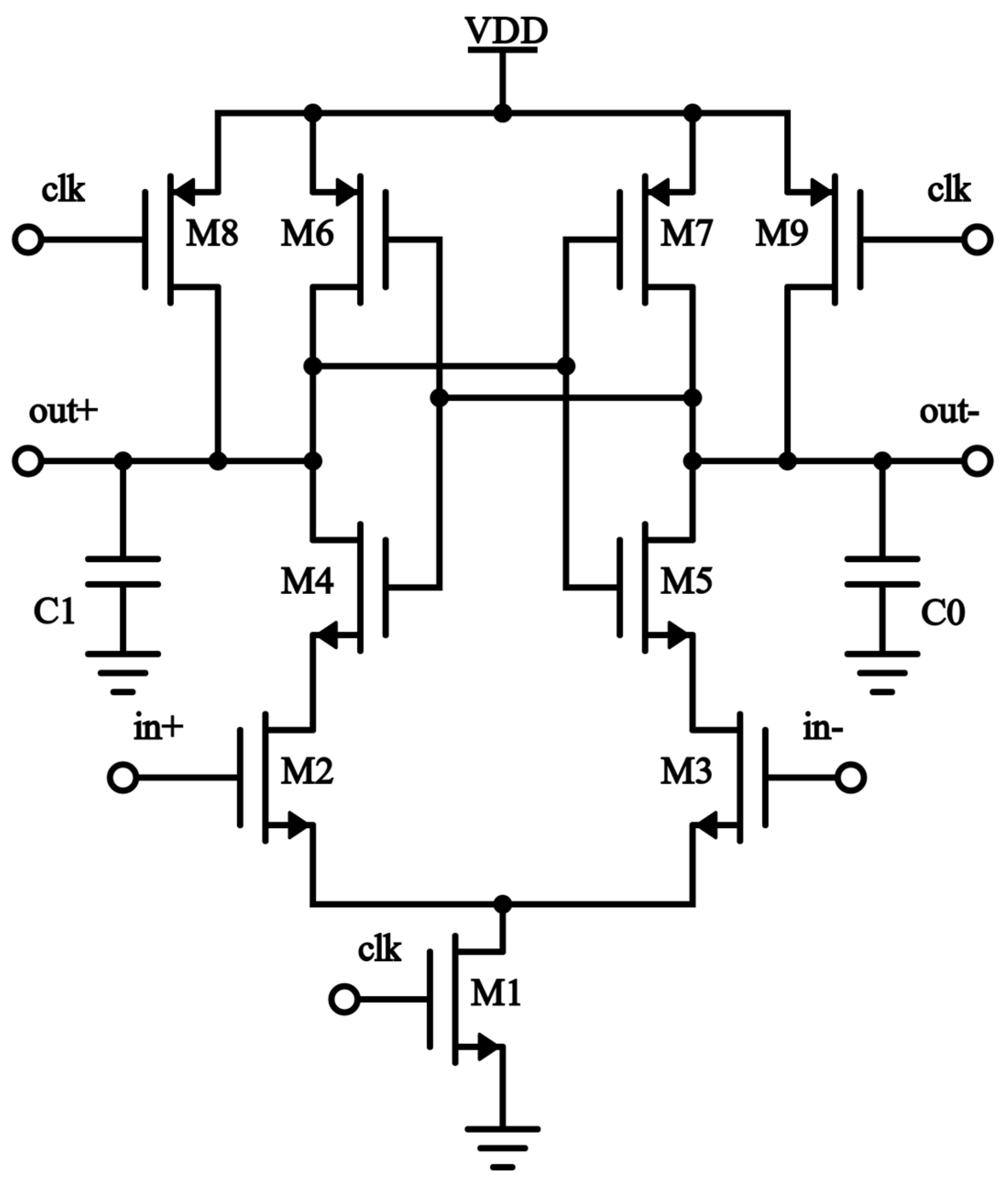
The operation of the conventional single-tail dynamic comparator depicted in
Figure 1 consists of two phases [
12]:
Reset phase: The reset phase starts when clk = 0. In this phase, the reset transistors and are on while the tail transistor is off. As a result, output nodes out+ and out− are pulled up to , which ensures the initial condition as well as a valid logic level for the comparator.
Comparison phase (decision-making phase): The comparison phase starts when clk = . In this phase, the reset transistors and are off while the tail transistor is on. The output nodes out+ and out−, previously precharged to , turn and on. Also, these two output nodes begin to discharge their voltages, which is still high enough to keep and on. The discharging rate of out+ and out− depends on the voltages at two input nodes in+ and in−.
When in+ > in−: Out+ discharges at a faster rate compared to out−. This means that the voltage at out+ drops to before out−, making turn on before . Since () and together form back-to-back inverters, the latch regeneration is activated. Hence, out+ and out− are pulled down to GND and pulled up to , respectively.
When in+ < in−: The circuit works in the opposite manner with the final result of out+ and out− being pulled up to and pulled down to GND, respectively.
In summary, during the comparison phase:
2.2. Delay Analysis
The propagation delay is one of the key features of a comparator. It consists of two parts:
Delay for the capacitors
and
to discharge to the point when
and
turn on:
where
is the load capacitor at the output nodes with equal values (i = 0, 1 and
);
is the threshold voltage of p-channel MOSFETs
; and
are the drain currents through
, respectively.
Delay from the two cross-coupled inverters:
Since the threshold voltage of the comparator is considered to be half of the supply voltage, or
, it means that
where
is the output voltage swing and
is the supply voltage.
Therefore, the latch delay is calculated as
where
is the equivalent transconductance of the latch and
is the output voltage difference.
Also, at time
:
where
is the drain current through
and
is the current difference at the input ends.
Since
:
where
are the current factors of
respectively.
The total delay is the sum of its two parts:
The simulation results illustrate that
dominates
[
1] and
follows the change in
. In other words, when
decreases,
increases and
hence increases, and vice versa.
2.3. Power Analysis
In order to prevent inaccuracies at boundaries between operating regions, instead of MOSFET’s existing models, its time-variant model is applied to analyze the power of the conventional dynamic comparator [
13]. The formula for drain current applicable to all operating regions is expressed in the work of [
14] as
where
is the gate–source potential difference,
is the threshold voltage,
is the drain–source potential difference, and
is the thermal voltage
.
and
are given by
where
is the body-effect coefficient,
is the gate-bulk potential difference,
is the threshold voltage with zero source-bulk voltage
,
, k is Boltzmann’s constant, q is the electron charge,
is the doping density of the subtrate, and
is the density of electrons in undoped silicon.
For one period of comparison, the average power of the supply voltage is calculated as
where
is the frequency of the comparator’s clock,
is the supply voltage, and
is the current drawn from the supply voltage.
When clk = 0 (reset phase), in order to charge the output nodes to , a current is drawn from the supply voltage source.
When clk =
(decision-making phase), assuming that in+ > in−, according to the working principle of the conventional dynamic comparator explained above,
will turn on before
. Since
has already been on, there is a current drawn from
from
. Therefore, during this comparison phase,
is equivalent to the current through
. Meanwhile, as the voltage at out− discharges to the ground,
will be off and there will be no current drawn from
. As a result, such a comparator is classified as dynamic [
13].
To calculate the average power during the comparison phase, we apply the time-variant model for current through
described in (8) to the formula in (11):
where the lower and upper bound of the integral in (12),
and
, respectively, are clarified in the delay analysis part.
For the integral in (12) to be solvable, it is necessary that the approximation when is used. Since the exponential terms of (12) are much larger than 1, the mentioned approximation is valid.
Simplifying the integral in (13), the closed-form expression for power is obtained as
where
and
(
is the equivalent transconductance of the latch as mentioned in the delay analysis).
For the case in+ < in−, power dissipation can be obtained by substituting
with
in the formula of (14):
2.4. Cadence Virtuoso Simulation
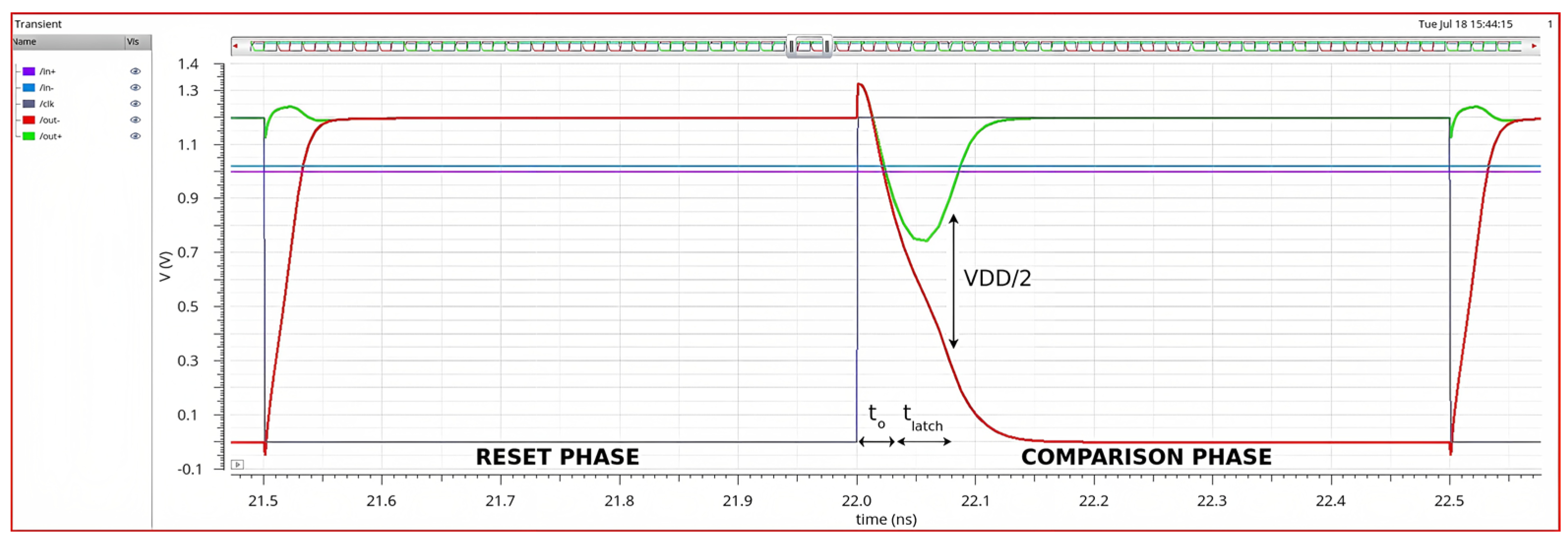
The conventional dynamic comparator is designed and simulated in the 65 nm technology of the TSMCN65 process. The frequency at which the circuit functions is = 1 GHz and the supply voltage is = 1.2 V. The voltage at node in− is constant at 1 V as a reference voltage, while in+ is a pulse voltage source with the maximum and minimum value of 1.005 V and 0.995 V, respectively, and a frequency of 100 MHz. With this input configuration, = 5 mV.
Figure 2 shows the transient simulation of the conventional comparator in one clock period that consists of both the comparison and the reset phase.
and
are the parameters explained above in
Section 2. The total propagation delay of the dynamic comparator is the sum of
and
in
Figure 2,
.
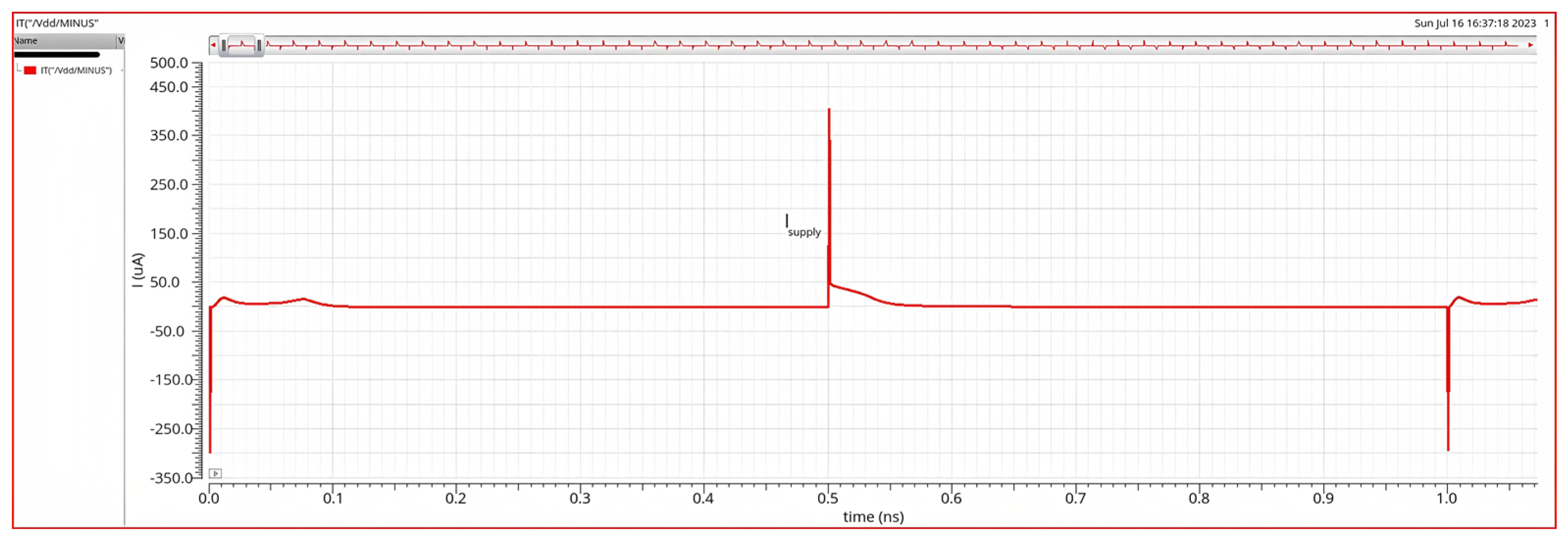
Figure 3 demonstrates the transient simulation of the current
drawn from the supply voltage
in one period from 0 to 1 ns. To calculate the power dissipation of the dynamic comparator, we integrate
with respect to time from 0 to 1 ns and multiply with
and
as in Equation (11) to obtain the result.
4. Results and Discussion
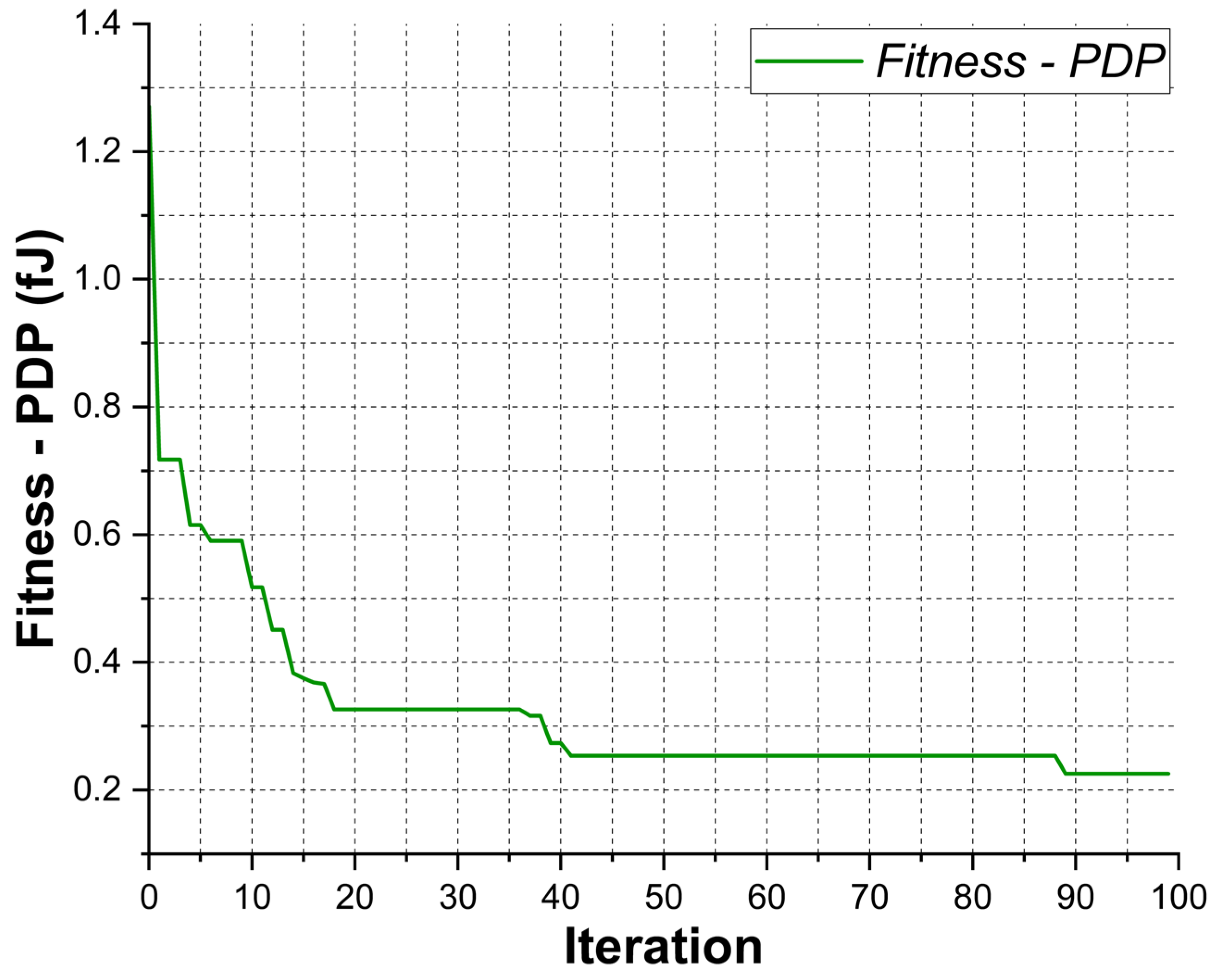
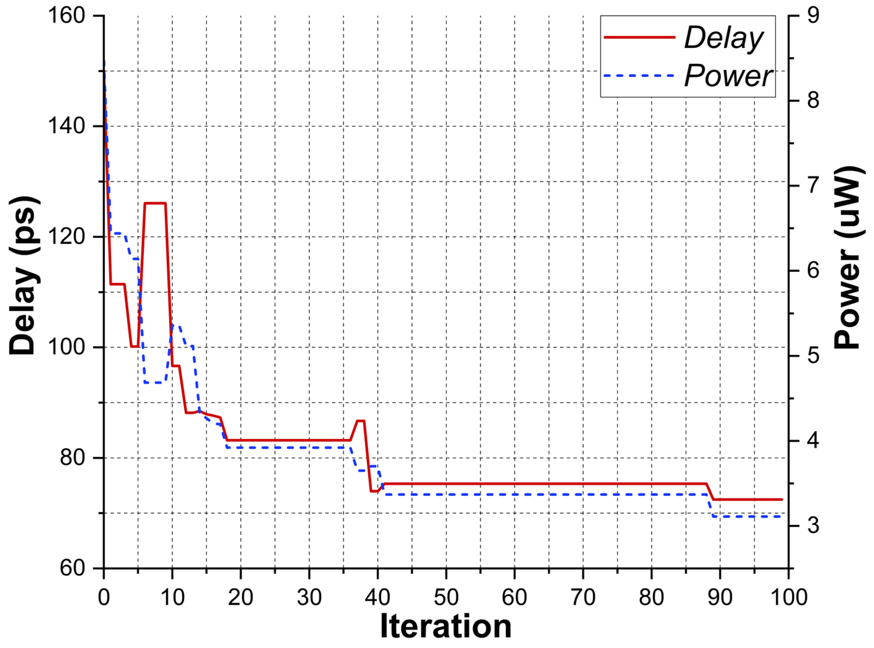
The simulation results indicate that the lowest value for PDP of 0.2254 fJ is achieved for the case of
= 0.8 and
= 0.05. With PDP = 0.2254 fJ, the delay and power of the conventional dynamic comparator are 72.48 ps and 3.11 µW, respectively. PDP fitness values as well as the delay and power over 100 iterations of GA are illustrated in
Figure 6 and
Figure 7, respectively.
As can be clearly observed in
Figure 7, the values for delay and power vary in an unpredictable and non-monotonous manner. However, their corresponding PDP in
Figure 6 decreases monotonously throughout the 100 iterations. Since GA produces chromosomes with better fitness values at the end of each iteration, PDP’s downward trend conforms to the working principle of the algorithm. In terms of the variables declared for GA, the optimal set
= (0.4463 µm, 0.1277 µm, 0.1553 µm, 0.1 fF) is obtained after 100 iterations of the algorithm. Nevertheless, it is worth noticing that the process grid of the TSMCN65 process is 5 nm. This means that the widths of
need to be rounded to their closest feasible values as
= (0.445 µm, 0.13 µm, 0.155 µm). Re-simulated results with the set
= (0.445 µm, 0.13 µm, 0.155 µm, 0.1 fF) vary slightly with the final values of 72.61 ps for delay, 3.11 µW for power consumption, and 0.2258 fJ for PDP.
The post-optimization sizes of all MOSFETs in the circuit are presented in
Table 1:
Table 2 summarizes the performance of the conventional dynamic comparator of this research and other research works:
As the conventional dynamic comparator in this work has zero static power consumption, its power consumption at 1 GHz is much lower than that of the circuit of [
10]. Since clock frequency is directly proportional to power dissipation as presented in Equation (11), the designs of [
8,
9,
11] with higher clock frequency exhibit a higher power than our design, which is reasonable. Meanwhile, the power consumption in [
1] is still lower despite operating at higher frequency. The parameter energy per conversion, which is equal to the ratio of power over sampling frequency (or clock frequency), is therefore needed to evaluate dynamic comparators’ performance with respect to power. From
Table 2, it is clear that our research work has the second-lowest energy per conversion value at 3.11 fJ per conversion.
In addition, compared to [
9,
10,
11], our work has approximately a 20% higher average delay. On the contrary, our average delay is less than one-fifth in comparison with the delay of [
1]. Because delay and power trade off with each other, PDP is utilized as the FoM in the case of optimizing both parameters. With respect to PDP, our design obtains the second-best value of 0.2258 fJ versus the lowest number of 0.0984 fJ by [
1].
For further assessment of our optimization system, the optimization platform of the Analog Design Environment (ADE) GXL, which offers both local and global optimization of circuit performances of interest, can be utilized as a suitable reference model. For setup steps, PDP is chosen as the optimization function, and the optimization variables and their bounds are similar to the GA-Spectre-based system. Regarding ADE GXL’s local optimization, the post-optimization transistors’ sizes = (0.445 µm, 0.13 µm, 0.155 µm, 0.1 fF) obtained from the GA-Spectre framework are set as the reference points. With regard to global optimization from ADE GXL, due to our constrained data, the C version Feasible Sequential Quadratic Programming (CFSQP) is selected by the Spectre simulator as the optimization algorithm. It is worth acknowledging that while the CFSQP utilizes a single individual for each iteration rather than a population of individuals, GA in our system is implemented on a population of six individuals per iteration. Hence, for a decent comparison, the PDP result of 100 iterations of our GA-based optimization system should be compared with that of 6 × 100 = 600 iterations of the ADE GXL’s global optimization tool.
Table 3 indicates that the result of PDP acquired by our optimization system is lower and has a higher convergence rate compared to that of ADE GXL’s local as well as global optimization tool.
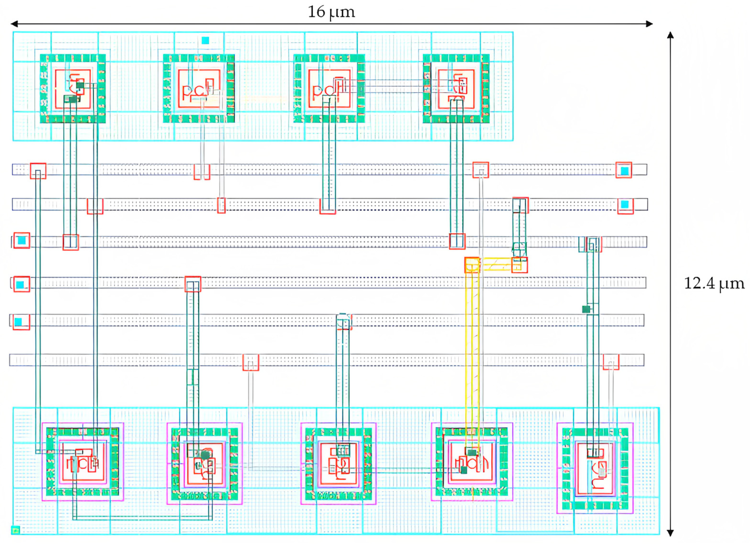
Figure 8 depicts the layout of the conventional dynamic comparator, which occupies an area of approximately 198.4 µ
(16 µm × 12.4 µm). Additionally,
Table 4 demonstrates layout parameters of different designs while
Table 5 represents a comparison between pre-layout and post-layout simulation results.


