Article

Adaptive Image Size Padding for Load Balancing in System-on-Chip Memory Hierarchy

Faculty of Applied Energy System, Electronic Engineering Major, Jeju National University, Jeju 63243, Republic of Korea
*
Author to whom correspondence should be addressed.
Electronics 2023, 12(16), 3393; https://doi.org/10.3390/electronics12163393
Submission received: 6 July 2023 / Revised: 6 August 2023 / Accepted: 8 August 2023 / Published: 9 August 2023
(This article belongs to the Section Computer Science & Engineering)

Abstract

:
The conventional address map often incurs traffic congestion in on-chip memory components and degrades memory utilization when the access pattern of an application is not matched with the address map. To reduce traffic congestion and improve the memory system performance, we propose an adaptive image size padding technique for a given address mapping and a hardware configuration. In the presented software approach, the system can adaptively determine the image pad size at the application-invoke time to enhance the load balancing across the on-chip memory hierarchy. Mainly targeting a high-bandwidth image processing application running in a device accelerator of an embedded system, we present the design, describe the algorithm, and conduct the performance experiment. As a result, the experiments indicate the presented design can improve load balancing up to 95% and performance up to 35%, with insignificant memory footprint overheads.

1. Introduction

In modern system-on-chip (SoC), the performance gap between a processor and memory is significant. This well-known gap, called the “memory wall”, is the growing disparity of speed between a processor and off-chip memory. To reduce this gap, modern SoCs internally accommodate multiple DRAM channels. To reduce row-buffer conflicts and better utilize the DRAM components, interleaving techniques are widely used [1,2,3,4,5,6,7,8]. Using such techniques, DRAM components can handle the transactions in parallel, balance traffic loads, and enhance system utilization. The state-of-the-art SoC accommodates multiple cache instances attached to a single processing unit. However, there has been little work taking both caches and the main memory into account. In this work, we present a systematic design method to enhance load balancing in the SoC memory hierarchy.
In an image processing application, pixels have their memory addresses. In practice, a linear address map (LIAM) is commonly used to associate a pixel and a memory address. We mainly target a 2D data (such as image processing) application as an example due to the following. First, image processing applications require high bandwidth and the load balancing is an important issue. Second, the traffic pattern is regular and known information. We use the known traffic pattern to efficiently configure the system. When the address pattern of memory traffics is linear, the traffic can be well interleaved across memory components. In certain scenarios, however, the traffic pattern is not linear and some memory components are not well utilized. Then, the system often does not achieve the expected bandwidth that the memory subsystem provides. To reduce the traffic congestion, dynamic memory mappings [9,10,11] or sophisticated interleaving schemes [12,13,14] are reported. Nevertheless, conventional methods require complex mapping schemes or hardware changes. To address this issue, we present the adaptive and efficient image size padding to enhance channel interleaving across the memory hierarchy. The presented design allocates additional memory space to exploit the master’s operation pattern and the system configuration. In the presented software approach, the device master can explicitly control the memory interleaving. Our approach combines the advantages of the simplicity of the conventional linear mapping and the configurability in the master. The main contributions of this paper are:
  • We propose the adaptive image size padding technique with the following features. First, the presented approach takes both caches and the main memory hierarchy into account. Second, the system can adaptively determine the image pad size at the application-invoke time. To develop the adaptive pad sizing algorithm, we conduct the metric analysis and derive the condition.
  • The design, the performance evaluation, and the overhead analysis are described. The experiments indicate the presented design can significantly enhance the traffic load balancing and the performance. Additionally, the analysis indicates that the memory footprint overhead is insignificant especially when the image is large sized.
This paper is organized as follows. In Section 2, related work is described. In Section 3 and Section 4, the conventional and the proposed designs are described. We present experimental results in Section 5 and draw the conclusion in Section 6.

2. Related Work

2.1. Dram Address Mapping

A number of techniques to reduce row-buffer conflicts in DRAM were reported. In ref. [1], an XOR permutation-based bank interleaving scheme is presented. In ref. [2], the memory map for the minimal open page is presented. In ref. [3], the bit-reversal memory mapping is presented. In ref. [4], to reduce DRAM row-buffer conflicts in a memory channel for a neural network accelerator, different banks have different memory mapping schemes. In ref. [5], a tool to uncover DRAM mapping is presented. In ref. [6], the impacts of the memory mapping on DRAM self-refresh power are analyzed. In ref. [7], the hardware-software collaborative address mapping to reduce row-buffer conflicts is presented. In ref. [8], a burst scheduling access reordering scheme for a 3D memory device is presented. Unlike [1,2,3,4,5,6,7,8], we present a pixel-to-address mapping scheme to enhance load balancing in cache and memory channels. In ref. [9], the dynamic re-arrangement of memory mapping to improve DRAM performance is presented. Our work is similar to [9] in that the mapping is determined in an adaptive way. In ref. [10], dynamic memory interleaving is controlled by the decoder. In ref. [11], the dynamic memory mapping to control the rank access pattern is presented. Unlike [9,10,11], we present a pixel-to-address mapping scheme determined at the application-invoke time.

2.2. Address Generation

In ref. [12], the rearrangeable hardware address map for DRAM bank interleaving is presented. Our metric analysis and adaptive address map are similar to [12]. Our work differs from [12] in that we present the image size padding (software) approach. In ref. [13], the address generation scheme for parallel interleaved architecture for the communication system is presented. In ref. [14], loop and data layout transformations for data access locality and reducing conflict cache miss are presented. In ref. [15], transposed matrix algorithms to enhance coalesced access and conflict-free bank access for GPU are presented. Unlike [13,14,15], we present the data-to-address mapping (transaction-level padding) scheme to enhance the traffic load balancing across memory hierarchy levels.

2.3. Image Applications and Deep Learning

In ref. [16], a deep-learning based assessment technique using human–computer interaction and virtual reality for mental health physical examination is presented. In ref. [17], the impact of hyperglycaemic crisis episodes on long-term outcomes for inpatients presenting with acute organ injury is presented. In ref. [18], the hyperspectral image classification method using deep learning is presented. Unlike [16,17,18], we present the address mapping scheme for the convolution, which is the key computation in deep learning.

2.4. Cache

In ref. [19], to reduce cache traffic congestion and enhance spatial locality between a GPU and a cache, the memory request prioritization and a grouping scheme are presented. In ref. [20], a tag-free page cache is presented. In ref. [20], when the non-cacheable bit is 0, virtual-cache mapping is used. When the cacheable bit is 1, a virtual-to-physical mapping is used. Our work is similar to [20] in that addresses are differently mapped depending on the cacheable and the non-cacheable attributes. Our work differs from [19,20] in that we present a pixel-to-address mapping scheme to enhance load balancing in cache and memory channels. In ref. [21], to reduce cache misses, execution instances of the vectored code are interleaved. Unlike [21], we present a cache interleaving scheme for load balancing.

2.5. Padding

The data (image) size padding itself is not a new idea. A number of data-size padding schemes to reduce cache conflict misses are presented. In ref. [22], a padding scheme for the convolution operation is presented. In ref. [23], the zero padding for the convolution operation is presented. Unlike [22,23], we present the memory allocation padding. In ref. [24], the compile-time data-layout transformation techniques mainly for software loop iterations are presented. To do that, the inter-variable padding (that adjusts a variable base address) and the intra-variable padding (that adjusts array dimension size) are presented. In ref. [25], an algorithm for array padding (increasing the size of array dimensions) is presented. In ref. [26], for a multiprocessor system, the inter-array padding among macro-tasks with a data localization scheme is presented. This method decomposes loops sharing the same arrays to fit cache size and executes the decomposed loops consecutively at the same processor. In ref. [27], a program transformation to reduce conflict misses for multi-level caches is presented. In ref. [28], parallel algorithms for integral image computation are presented. The implementation in [28] aims to reduce bank conflicts by adding a variable amount of padding to each shared memory index. In ref. [29], the scheme utilizing a single instruction multiple data (SIMD) and an array padding technique to reduce the memory bank conflict are introduced. Unlike [24,25,26,27,28,29], we present the adaptive scheme configured at the application-invoke time to enhance the load balancing across the memory hierarchy.

3. Background

In this section, design conventions, traditional linear mapping methods, and motivational examples are reviewed. We mainly target embedded systems where device accelerators run high-bandwidth 2D data applications. Table 1 shows design parameters. The example values are used in this section.

3.1. Transaction and Memory Attributes

Figure 1 depicts an example SoC organization where there are four cache instances and four memory channels. An I/O (Input/Output) device master such as a camera controller operates at the pixel coordinate level. A master accesses memory uses transactions. A transaction is memory access. It consists of read and write channels. In both channels, there are pre-defined request and response hardware signals to deliver the transaction. The transaction contains address, data, and control information. If an image pixel is an RGB format, a pixel is 4-byte sized. When the transaction size (TranSize) is 64 bytes, a transaction accesses 16 RGB pixel data. Typically, a transaction requires significant latency to access memory. Accordingly, a master issues multiple requests before their responses return back to the master. This is called multiple outstanding [30]. This is widely used in a modern SoC because it significantly improves the throughput performance. As an example, if a master issues four requests (before their responses arrive at the master), the multiple outstanding count is 4.
When an application is invoked, an operating system (OS) allocates memory space. When an image size is 128 × 32 pixels, 16,384 (=128 × 32 × 4) bytes of memory is allocated. Different applications have different memory attributes. When a single master (the image processing unit) operates a 2D data application and the application has certain data localities, OS sets the allocated memory as cacheable. In this case, transactions can be stored in on-chip system caches, as depicted in Figure 1. On the other hand, in the camera preview application, a camera controller captures an image and the display controller displays the image in the raster-scan order. A raster scan is a method of constructing an image through the use of horizontal lines by starting in the upper left-hand corner of the screen and drawing a horizontal line that ends on the right edge of the screen. In this scenario, multiple masters (the camera and the display controllers) communicate data using shared main memory, as depicted with the dotted line. In this case, the OS sets allocated memory space as non-cacheable. In practice, a cache line and a transaction are usually the same size.

3.2. Address Mapping

Image pixels are mapped onto their unique address numbers and memory locations. To do this, three mapping steps are required.
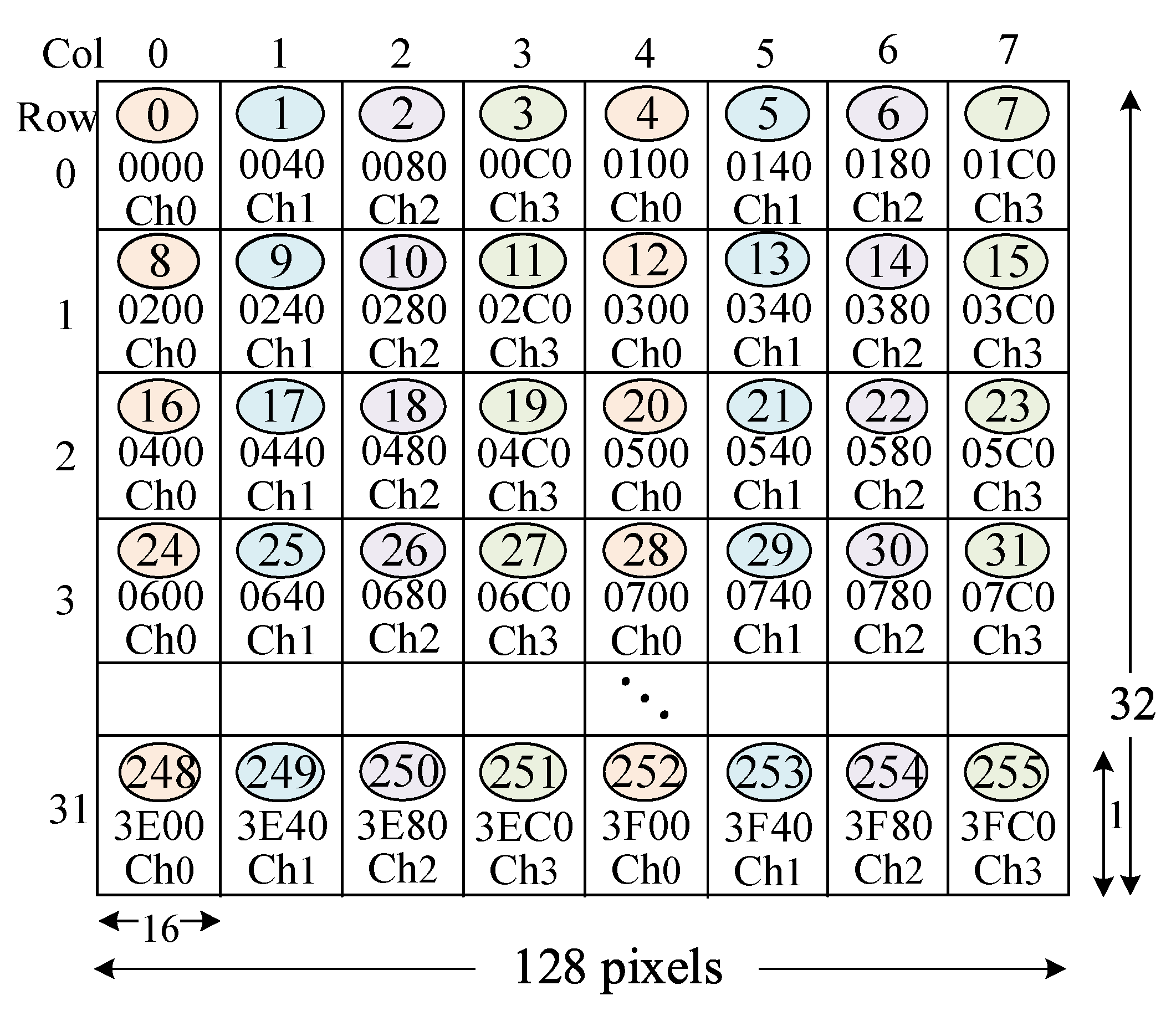
  • An address map converts image pixels onto their transaction addresses. Figure 2 depicts the linear address map (LIAM) for the image with 128 × 32 pixels. In Figure 2, the transaction addresses sequentially increase in the horizontal direction. This conventional method is widely used in practice due to its simplicity. The number in the circle is the transaction number that indicates the order of the addresses. A single transaction accesses 64 bytes of data or 16 RGB pixels. Suppose a master generates the transaction ➈ to access the pixel coordinate (16, 1). Then, the transaction address is 240 in the hexadecimal number.
  • A cache map converts an address onto a tag, an index, a channel, and an offset number. Figure 3a depicts an example in which the cache line size is 64 bytes. The address 240 for the transaction ➈ is mapped to the cache channel 1 as denoted by Ch1.
  • A memory map converts the transaction address onto a DRAM location (a row, a bank, a channel, and a column number). Figure 3b depicts an example. The address 240 for the transaction ➈ is mapped to the DRAM channel 1.
In Figure 2, when the address pattern is linear or raster scan, the traffic pattern is well matched with LIAM. In Figure 2, suppose the address patterns are Electronics 12 03393 i001, ➀, ➁, and ➂, then the targeted channels are Ch0, 1, 2, and 3. This means the outstanding transactions desirably access memory components in the interleaved and the load-balanced way.

3.3. Motivational Use Cases

The memory performance is significantly affected by address patterns. When the traffic pattern is not linear, the traffic is not well matched with LIAM. An example is an image rotation application. When a camera captures an image in the landscape mode and displays the image in portrait mode, the image should be rotated. In this case, the traffic accesses an image in the vertical direction. In Figure 2, suppose the address patterns are Electronics 12 03393 i001, ➇, ⑯, and so on, and thus, the targeted channels are Ch0, 0, 0, and so on. This means the outstanding transactions access a single component and incur the congestion. However, a single component can serve a single transaction at a time. Subsequently, the traffic congestion incurs undesirable delay and degrades memory performance.
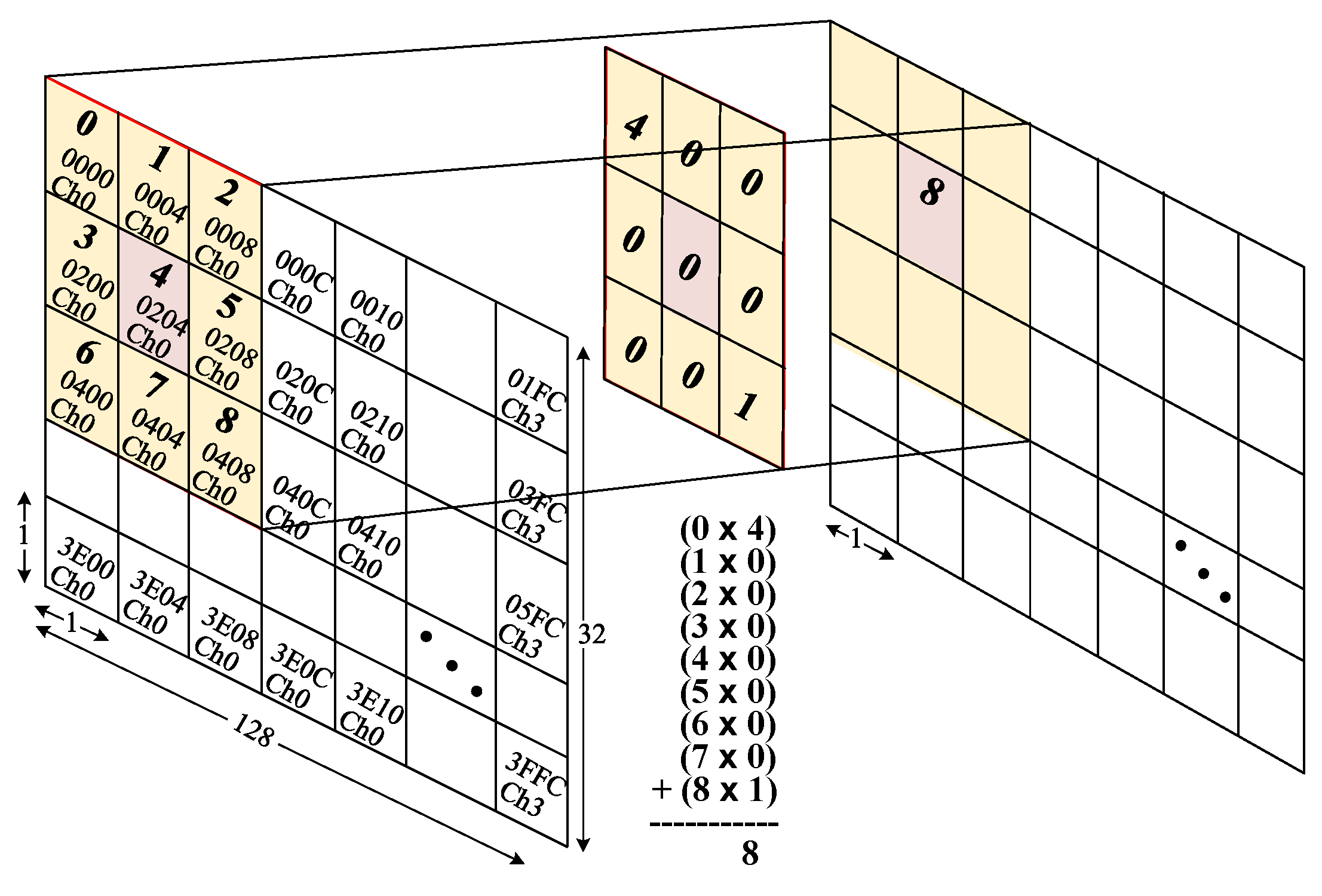
Another example is a convolution operation. Convolution is one of the fundamental image processing operators processed at the block level. The convolution is performed by sliding the kernel over the image to move the kernel through all the positions where the kernel fits entirely within the boundaries of the image. The output image pixel values are calculated by multiplying each kernel value by the corresponding input image pixel values. In Figure 4, a block with 3 × 3 pixels is processed in the convolved way. To access the rectangle block, three transactions access the channel 0. This is undesirable because those outstanding transactions access the same cache and incur the congestion. To alleviate this congestion problem, we present the design that can enhance load balancing in the next section.

4. Proposed Design

4.1. Overview

We mainly target embedded systems where device accelerators run high-bandwidth 2D data applications. The presented approach is summarized by the following. First, we conduct the metric analysis and identify the condition where the conventional LIAM is undesirable. Second, when an application is invoked, the device driver checks the condition. If the condition is met, the device driver conducts the image size padding by allocating additional memory. If the condition is not met, the device driver uses the conventional LIAM. In the subsequent sections, the details are described.

4.2. Liam Metric Analysis

To reduce traffic congestions, it is desired that outstanding transactions access different channels in the interleaved way. To quantify the interleaving, we define the relative metric as follows:
Metric a d j = 1 , if different channel accessed 0 , if same channel accessed
where Metric a d j denotes a relative metric between the adjacent transactions. Metric a d j can be 1 (desirably interleaved) or 0 (undesirable). Our metric analysis is similar to [12]. However, our metric is defined for (cache or memory) channel interleaving, whereas the metric in [12] is defined for DRAM bank interleaving. Additionally, multiple outstanding is not taken into account in [12]. Considering multiple outstanding, we define a metric for a transaction (column i and row j) as follows:
Metric i , j = N , S , E , W m = 1 M 1 Metric a d j
where M denotes a multiple outstanding count. We calculate Metric i , j by adding Metric a d j between M 1 neighbors in the northern (N), the southern (S), the eastern (E), and the western (W) directions.
Example 1.
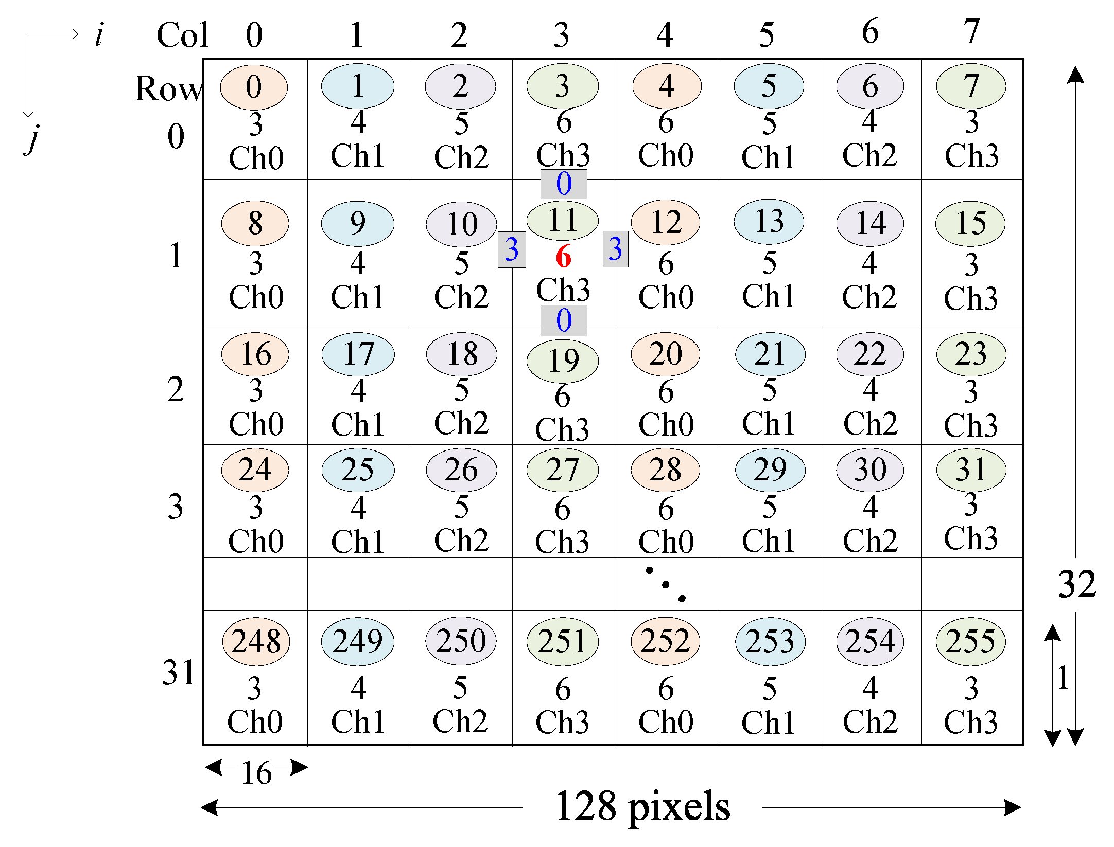
Suppose a master sends four outstanding transactions ⑪, ⑫, ⑬, and ⑭. Metric a d j between (⑪, ⑫),(⑪, ⑬),(⑪, ⑭) in the eastern direction is 1,1,1. Then, Metric 3 , 1 of the transactionin the eastern direction is 3 (=1 + 1 + 1). Similarly, Metric 3 , 1 in the other directions can be calculated as depicted in the shaded rectangles in Figure 5. Accordingly, Metric 3 , 1 for the transactionis 6 (=0 + 0 + 3 + 3).
Finally, the average metric is calculated by:
Average metric = i , j Metric i , j Total number of transactions
In Figure 5, total number of transactions is 256. Then the average metric is calculated by 5.9 (= 3 + 4 + 5 + + 3 256 ). To identify the relationship between interleaving, image size, and memory system configuration, we define the super-line size (SLS) calculated by:
SLS = LineSize × NumCacheCh ( if an attribute is cacheable ) TranSize × NumMemCh ( if an attribute is non - cacheable )
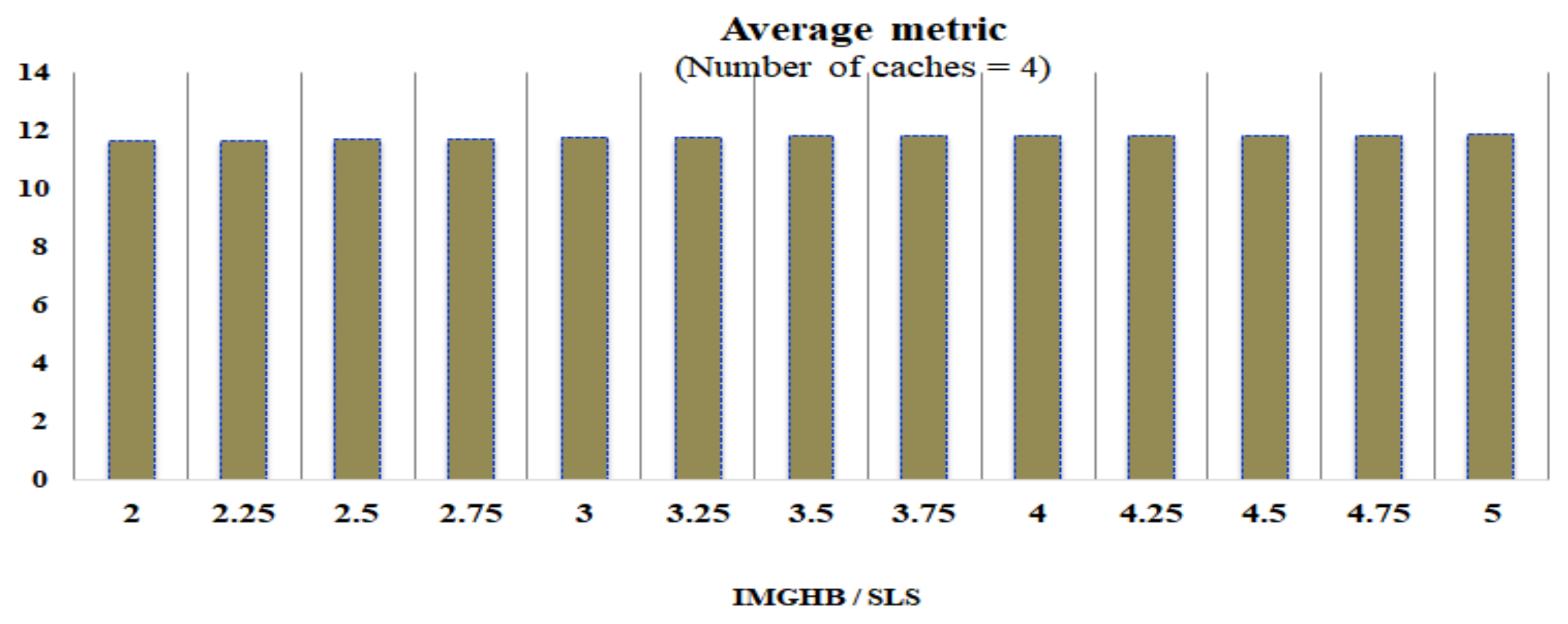
As an example, if there are four memory channels and the transaction size is 64 bytes, SLS is 256 (=4 × 64) bytes. Figure 6 depicts the average metric versus I m g H B S L S values. The I m g H B S L S value indicates the image horizontal size for a given system memory configuration. In Figure 6, the higher metric indicates better interleaving. Figure 6 suggests that the metric is lower or undesirable when the following condition is met:
p 2 1 8 < I m g H B S L S < p 2 + 1 8 , ( p is natural integer )
As an example, when I m g H B S L S is within the ranges [1.875, 2.125], [2.375, 2.625], [2.875, 3.125], and so on, the metric is undesirably low. If this condition is true, LIAM gives undesirable interleaving. When SLS is 2 n bytes, Equation (5) can be efficiently implemented by checking ImgHB[ n 2 : n 3 ]. If these two bits are 00 2 or 11 2 , the condition in Equation (5) is true.

4.3. Padded Linear Address Map

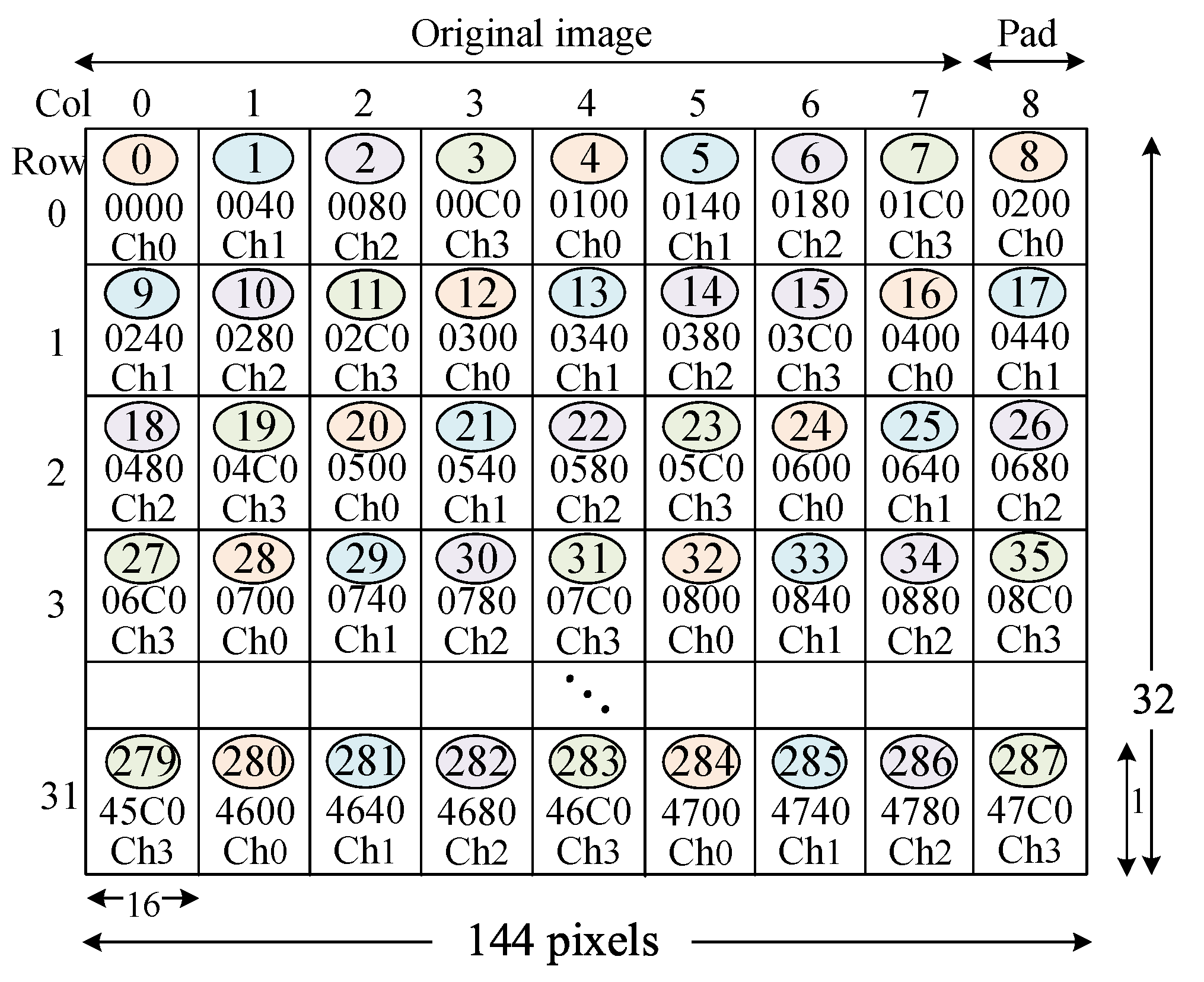
We identified the condition in Equation (5) where LIAM is undesirable. To improve the memory load balancing, we present the padded address map. Our design goal is that adjacent outstanding transactions access different memory components such that the performance penalty due to traffic congestion is reduced. This can be efficiently achieved by padding horizontal image size or allocating additional memory. Figure 7 depicts the example of the padded address map where the horizontal image size increases by a transaction size. When the access pattern is vertical, the targeted channels are Ch0, 1, 2, 3, and so on. We call this a padded linear address map (pLIAM). The main novel features of pLIAM are:
  • An image size padding technique is applied in the adaptive way, taking both caches and the main memory hierarchy into account.
  • The system can adaptively determine the image pad size at the application-invoke time.

4.4. Adaptive Pad Sizing

Figure 8 depicts the pad sizing algorithm where the padding is conducted when an access pattern is not linear and when Equation (5) is true. To determine the pad size, a sophisticated method can be developed taking the channel interleaving into account. However, to simplify the design, we determine the pad size by a transaction size considering that a single transaction is a minimum granularity to access memory. If the original image horizontal size (ImgH) is 128 pixels and a transaction size is 64 bytes (or 16 RGB pixels), then the padded ImgH will be 144 (=128 + 16) pixels. Figure 9 depicts the pLIAM average metric for Figure 7 when the algorithm is applied. As clearly depicted in Figure 9, the average metric is significantly higher than the LIAM metric in Figure 6. This means pLIAM can improve interleaving and load balancing. Table 2 shows the pad sizing examples. Given an image size, if the I m g H B S L S value meets Equation (5), the padding is conducted. The main disadvantage of our design is the memory footprint overhead. The memory footprint refers to the amount of main memory that an application uses while running. In Figure 7, the padded space (for column 8) is allocated but it is not used. Accordingly, 18,432 (=144 × 32 × 4) bytes of memory is allocated. In this case, 13% more memory space than LIAM is required. In other words, the footprint overhead is 13%, which is significant. However, as further described later in Section 5, the memory overhead decreases when an image size increases. The computation complexity of the proposed method is the constant time or O(1). This is because the algorithm depicted in Figure 8 can be implemented using three “if” statements without any iterations.

4.5. System Configuration Furthermore, Operation

The hardware memory organization (the number of cache and memory channels) is determined at the design time. The address mapping scheme (Figure 3) is determined at design time or reset time. In an embedded system, the traffic pattern of an application is typically the known information. Figure 10 depicts the system operation. When an application is invoked, the information on the I m g H B S L S value and an access pattern is available. Using this information, the OS checks Equation (5), determines the image pad size, and allocates memory. Then, the OS sets the cacheability attributes of the allocated memory and initiates the hardware master. When this information is set, the application runs in the hardware system.

5. Experimental Results

To experiment with the presented designs, we modified the system performance model in [12] to support multiple caches and memory channels previously depicted in Figure 1. The components communicate with each other using the AXI bus protocol [30]. To support channel interleaving, we implemented the re-order buffer model in the interconnect. We implemented the pad sizing algorithm in C++ and integrated it into the system model. Table 3 shows the configuration.
Table 4 shows workload scenarios. In camera preview, a camera controller captures an image and displays it. In image scaling, an image is resized. In image blending, two images are blended and a composite image is created. In these workloads, an access pattern is raster scan or linear. In this case, an image size padding is not conducted. On the other hand, there are a number of applications such as rotation and reversing that access an image in a non-linear manner. In this paper, we mainly consider these workloads because they are widely used in modern mobile devices. In these non-cacheable (denoted by NC) workloads, masters communicate each other using the shared main memory and the address pattern has little localities. Edge detection and convolution operate at the block level. These applications have relatively high address localities and have cacheable (denoted by C) attributes. The memory access behaviors of these workloads are implemented in the master model in the system. In Table 4, the pad size is 0 or TranSize. Based on the algorithm previously depicted in Figure 8, the pad size is TranSize when the condition is met. Otherwise, the pad size is 0.
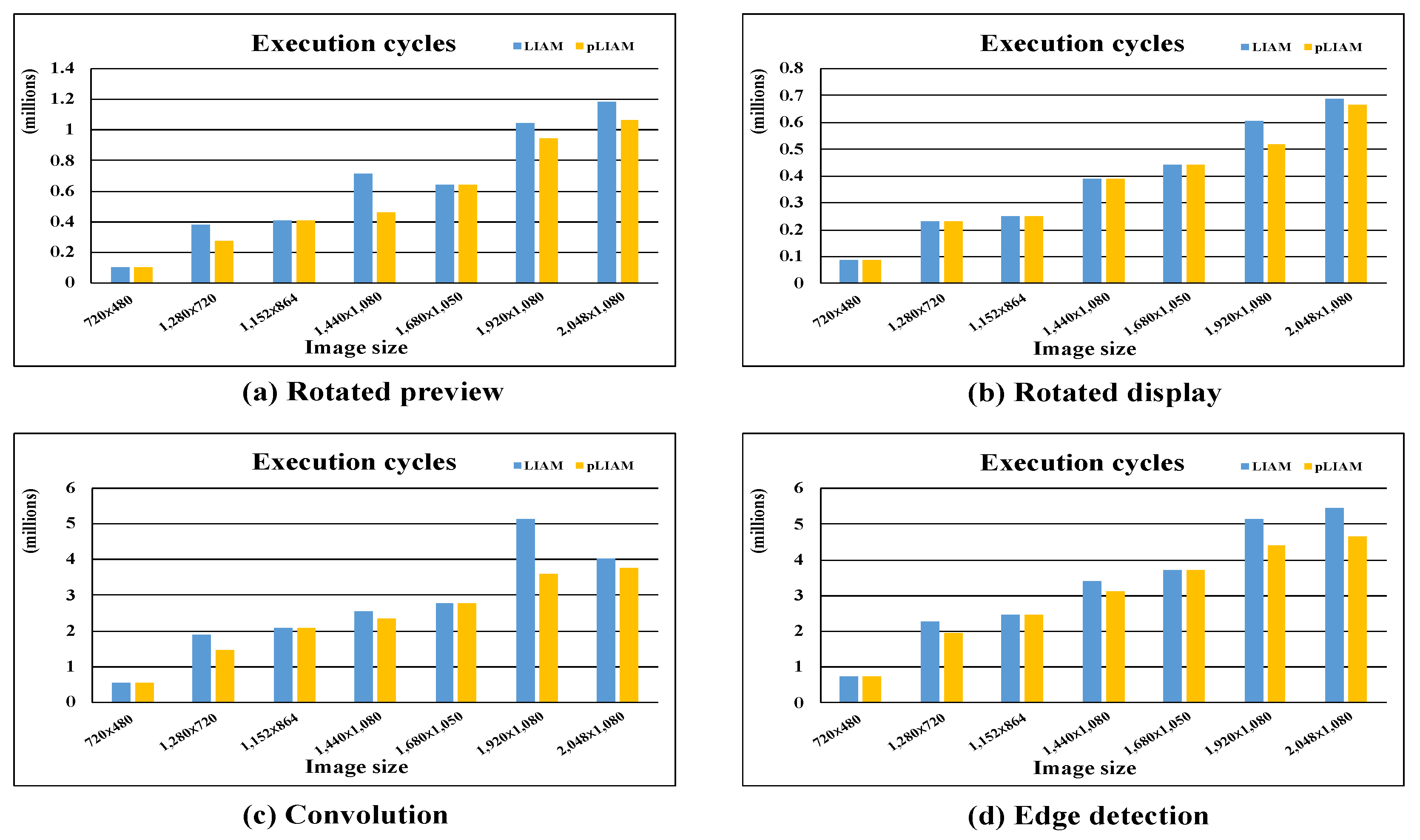
We conduct three experiments. First, to evaluate the performances of the workloads, we measure execution cycles. Figure 11 depicts the results. In workloads with linear access patterns, the pad size is 0. Then, pLIAM and LIAM are identical. In workloads with non-linear access patterns, the performance varies with the I m g H B S L S value. When the image sizes are 720 × 480 and 1680 × 1050, the pad size is 0. In other image sizes, 16 pixels are padded. It is noted that the performance is additionally affected by memory scheduling, bank access patterns, memory mappings, cache mappings, and so on. Accordingly, in some cases, the performance differences between pLIAM and LIAM are insignificant. Overall, however, pLIAM tends to improve the performance. In rotated preview, rotated display, edge detection, and convolution, pLIAM is up to 35%, 14%, 30%, and 15%, respectively, better than LIAM. This is mainly because of the load balancing in the memory components. Additionally, we conducted an experiment on the different configuration. Figure 12 depicts the performance results when there are four cache channels and two memory channels. As in the previous experiment, the same algorithm depicted in Figure 8 is applied. As a result, the performance is significantly improved. In rotated preview, rotated display, edge detection, and convolution, pLIAM is up to 39%, 32%, 37%, and 13%, respectively, better than LIAM. We experimented with other image sizes and obtained similar results. Our approach is generic in that other experimental setups do not require different solutions.
Second, to evaluate the load balancing, we measure the number of outstanding requests in a cache or a memory channel for an image size of 1920 × 1080 pixels. To quantify the load, we measure the number of on-going transactions in a request queue in every 20 cycles. When the number of outstanding requests in a channel is 0, the memory component is idle. To balance the loads, the deviations between the channels should be small. Figure 13 and Figure 14 depict the number of outstanding requests in non-cacheable workloads. Figure 13a and Figure 14a depict the undesirably balanced loads in LIAM. As an example, in cycle 15,000 of Figure 13a, cache channel 2 serves 15 outstanding transactions while the other channels are idle. This is undesirable because traffic congestion occurs in the channel 2. Figure 14a,b clearly depict the desirably balanced loads in pLIAM. As an example, in Figure 14b, the loads are evenly distributed in all channels. Figure 15 and Figure 16 depict the loads in cacheable workloads. Figure 15a and Figure 16a depict the undesirably balanced loads in LIAM. Figure 15b and Figure 16b depict the desirably balanced loads in pLIAM.
To quantify the load balancing, we measure the averages and standard deviations of the number of outstanding requests in Figure 13, Figure 14, Figure 15 and Figure 16. Table 5 shows the average numbers measured during the entire execution time. As a result, each channel handles a similar number of requests overall. However, to better balance the load and reduce the traffic congestion, it is important to reduce the deviations during the short period of time. Table 6 shows the standard deviations measured every 500 cycles. The lower the deviation is, the better balanced the load is. As a result, pLIAM improves load balancing up to 95%.
Third, we measure the memory footprint overheads with various image sizes. Figure 17 depicts the result. When an image size is 500 × 480 with 8 channels, pLIAM has 13% footprint overhead and it is significant. However, when an image size increases, the overheads tend to decrease. When the number of memory channels is 4, the overheads are 0.6% for an RGB format and 2.2% for a YUV format on average. When the number of memory channels is 8, the overheads are 0.8% for a RGB format and 3.1% for a YUV format on average. Overall, the overhead is 1.6%, which is insignificant.

6. Conclusions

  • Summary
The memory system performance is significantly affected by the address patterns and the load distributions. In this work, to enhance the load balancing across the memory hierarchy in SoC, we presented the image size padding scheme. The pad size is determined by the traffic address pattern, image size, hardware memory configuration, and allocated memory attributes. We presented two advantages (memory utilization and performance) and one overhead (memory footprint).
  • Memory utilization and performance
First, the presented design can improve memory utilization using the load balancing technique and memory interleaving. By adaptively padding the image size, the memory traffic can achieve better interleaving. Second, when the image size is sufficiently large and the traffic address pattern is non-linear, performance can be improved.
  • Overhead, limitation, and future work
The presented design can require the additional memory footprint. Though the presented scheme has certain memory allocation overheads, the overheads decrease when the image size increases. The overhead can be traded with improved performance. In this work, we focus on the address mapping for 2D data for a special-purpose I/O device accelerator in an embedded system. Accordingly, the application of our design is limited to high-bandwidth 2D data (for example, image processing) application. The address mapping for a multipurpose or general system where the address pattern is unknown can be further investigated. To generalize the solution, a sophisticated hardware design to detect the traffic pattern can be further developed. We leave these investigations for future research.

Author Contributions

Conceptualization, S.-Y.K. and J.-Y.H.; methodology, J.-Y.H.; investigation, S.-Y.K.; writing—original draft preparation, S.-Y.K. and J.-Y.H.; software, S.-Y.K. and J.-Y.H.; funding acquisition, J.-Y.H.; validation, S.-Y.K.; writing—original draft, S.-Y.K.; writing—review and editing, J.-Y.H. All authors have read and agreed to the published version of the manuscript.

Funding

This work was supported by the research grant of Jeju National University in 2021.

Data Availability Statement

The data used to support the finding of this study are included in the article.

Conflicts of Interest

The authors declare no conflict of interest.

References

  1. Zhang, Z.; Zhu, Z.; Zang, Z. Breaking address mapping symmetry at multi-levels of memory hierarchy to reduce DRAM row-buffer conflicts. J. Instr.-Level Parallelism 2001, 3, 29–63. [Google Scholar]
  2. Kaseridis, D.; Stuecheli, J.; John, L.K. Minimalist open-page: A DRAM page-mode scheduling policy for the many-core era. In Proceedings of the 44th Annual IEEE/ACM International Symposium on Microarchitecture, Porto Alegre, Brazil, 3–7 December 2011; pp. 24–35. [Google Scholar]
  3. Shao, J.; Davis, B.T. The bit-reversal SDRAM address mapping. In Workshop on Software and Compilers for Embedded Systems; Association for Computing Machinery: New York, NY, USA, 2005; pp. 62–71. [Google Scholar]
  4. Wei, R.; Li, C.; Chen, C.; Sun, G.; He, M. Memory access optimization of a neural network accelerator based on memory controller. Electronics 2021, 4, 438. [Google Scholar] [CrossRef]
  5. Wang, M.; Zhang, Z.; Cheng, Y.; Nepal, S. Dramdig: A knowledge-assisted tool to uncover dram address mapping. In Proceedings of the 2020 57th ACM/IEEE Design Automation Conference (DAC), San Francisco, CA, USA, 20–24 July 2020; pp. 1–6. [Google Scholar]
  6. Zhu, Z.; Cao, J.; Li, X.; Zhang, J.; Xu, Y.; Jia, G. Impacts of memory address mapping scheme on reducing DRAM self-refresh power for mobile computing devices. IEEE Access 2018, 6, 78513–78520. [Google Scholar] [CrossRef]
  7. Islam, M.; Shaizeen, A.G.A.; Jayasena, N.; Kotra, J.B. Hardware-Software Collaborative Address Mapping Scheme for Efficient Processing-in-Memory Systems. U.S. Patent 11,487,447 B2, 1 November 2022. [Google Scholar]
  8. Shao, J.; Davis, B.T. A Burst Scheduling Access Reordering Mechanism. In Proceedings of the 2007 IEEE 13th International Symposium on High Performance Computer Architecture, Scottsdale, AZ, USA, 10–14 February 2007; pp. 285–294. [Google Scholar]
  9. Ghasempour, M.; Jaleel, A.; Garside, J.D.; Luján, M. Dream: Dynamic re-arrangement of address mapping to improve the performance of drams. In Proceedings of the International Symposium on Memory Systems, Alexandria, VA, USA, 3–6 October 2016; pp. 362–373. [Google Scholar]
  10. Cypher, R.E. System and Method for Dynamic Memory Interleaving and De-Interleaving. U.S. Patent No. 7,318,114, 8 January 2008. [Google Scholar]
  11. Sato, M.; Han, C.; Komatsu, K.; Egawa, R.; Takizawa, H.; Kobayashi, H. An energy-efficient dynamic memory address mapping mechanism. In Proceedings of the 2015 IEEE Symposium in Low-Power and High-Speed Chips (COOL CHIPS XVIII), Yokohama, Japan, 13–15 April 2015; pp. 1–3. [Google Scholar]
  12. Hur, J.Y.; Rhim, S.W.; Lee, B.H.; Jang, W. Adaptive Linear Address Map for Bank Interleaving in DRAMs. IEEE Access 2019, 7, 129604–129616. [Google Scholar] [CrossRef]
  13. Chavet, C.; Coussy, P.; Urard, P.; Martin, E. Static address generation easing: A design methodology for parallel interleaver architectures. In Proceedings of the 2010 IEEE International Conference on Acoustics, Speech and Signal Processing, Dallas, TX, USA, 14–19 March 2010; pp. 1594–1597. [Google Scholar]
  14. Lin, H.; Wolf, W. Co-design of interleaved memory systems. In Proceedings of the Eighth International Workshop on Hardware/Software Codesign; Association for Computing Machinery: New York, NY, USA, 2000; pp. 46–50. [Google Scholar]
  15. Khan, A.; Al-Mouhamed, M.; Fatayar, A.; Almousa, A.; Baqais, A.; Assayony, M. Padding Free Bank Conflict Resolution for CUDA-Based Matrix Transpose Algorithm. In Proceedings of the 15th IEEE/ACIS International Conference on Software Engineering, Artificial Intelligence, Networking and Parallel/Distributed Computing (SNPD), Las Vegas, NV, USA, 30 June–2 July 2014; pp. 1–6. [Google Scholar]
  16. Li, M.; Zhang, W.; Hu, B.; Kang, J.; Wang, Y.; Lu, S. Automatic Assessment of Depression and Anxiety through Encoding Pupil-wave from HCI in VR Scenes. Acm Trans. Multimed. Comput. Commun. Appl. 2022. [Google Scholar] [CrossRef]
  17. Duan, Z.; Song, P.; Yang, C.; Deng, L.; Jiang, Y.; Deng, F.; Jiang, X.; Chen, Y.; Yang, G.; Ma, Y.; et al. The impact of hyperglycaemic crisis episodes on long-term outcomes for inpatients presenting with acute organ injury: A prospective, multicentre follow-up study. Front. Endocrinol. 2022, 13, 1057089. [Google Scholar] [CrossRef] [PubMed]
  18. Chen, H.; Wang, T.; Chen, T.; Deng, W. Hyperspectral Image Classification Based on Fusing S3-PCA, 2D-SSA and Random Patch Network. Remote Sens. 2023, 15, 3402. [Google Scholar] [CrossRef]
  19. Jia, W.; Shaw, K.A.; Martonosi, M. MRPB: Memory request prioritization for massively parallel processors. In Proceedings of the 2014 IEEE 20th International Symposium on High Performance Computer Architecture (HPCA), Orlando, FL, USA, 15–19 February 2014; pp. 272–283. [Google Scholar]
  20. Lee, Y.; Kim, J.; Jang, H.; Yang, H.; Kim, J.; Jeong, J.; Lee, J.W. A fully associative, tagless DRAM cache. ACM Sigarch Comput. Archit. News 2015, 43, 211–222. [Google Scholar] [CrossRef]
  21. Fang, Z.; Zheng, B.; Weng, C. Interleaved multi-vectorizing. Proc. VLDB Endow. 2019, 13, 226–238. [Google Scholar] [CrossRef]
  22. Wu, S.; Wang, G.; Tang, P.; Chen, F.; Shi, L. Convolution with even-sized kernels and symmetric padding. Adv. Neural Inf. Process. Syst. 2019, 32, 1194–1205. [Google Scholar]
  23. Hashemi, M. Enlarging smaller images before inputting into convolutional neural network: Zero-padding vs. interpolation. J. Big Data 2019, 6, 98. [Google Scholar] [CrossRef] [Green Version]
  24. Rivera, G.; Tseng, C.W. Data transformations for eliminating conflict misses. In Proceedings of the ACM SIGPLAN Conference on Programming Language Design and Implementation, Montreal, QC, Canada, 17–19 June 1998; pp. 38–49. [Google Scholar]
  25. Hong, C.; Bao, W.; Cohen, A.; Krishnamoorthy, S.; Pouchet, L.N.; Rastello, F.; Ramanujam, J.; Sadayappan, P. Effective Padding of Multidimensional Arrays to Avoid Cache Conflict Misses. ACM SIGPLAN Not. 2016, 51, 129–144. [Google Scholar] [CrossRef] [Green Version]
  26. Ishizaka, K.; Obata, M.; Kasahara, H. Cache Optimization for Coarse Grain Task Parallel Processing Using Inter-Array Padding. In Languages and Compilers for Parallel Computing: 16th International Workshop, LCPC 2003, College Station, TX, USA, 2–4 October 2003; Revised Papers 16; Springer: Berlin/Heidelberg, Germany, 2004; pp. 64–76. [Google Scholar]
  27. Vera, X.; Llosa, J.; González, A. Near-Optimal Padding for Removing Conflict Misses. In Languages and Compilers for Parallel Computing: 15th Workshop, LCPC 2002, College Park, MD, USA, 25–27 July 2002; Revised Papers 15; Springer: Berlin/Heidelberg, Germany, 2002; pp. 329–343. [Google Scholar]
  28. Bilgic, B.; Horn, B.K.; Masaki, I. Efficient integral image computation on the GPU. In Proceedings of the 2010 IEEE Intelligent Vehicles Symposium, La Jolla, CA, USA, 21–24 June 2010; pp. 528–533. [Google Scholar]
  29. Zhang, Q.; Li, Q.; Dai, Y.; Kuo, C.C. Reducing memory bank conflict for embedded multimedia systems. In Proceedings of the 2004 IEEE International Conference on Multimedia and Expo (ICME) (IEEE Cat. No.04TH8763), Taipei, Taiwan, 27–30 June 2004; Volume 1, pp. 471–474. [Google Scholar]
  30. ARM Architecture Reference Manual, ARMv8-A Edition. Available online: Http://www.arm.com (accessed on 20 May 2023).
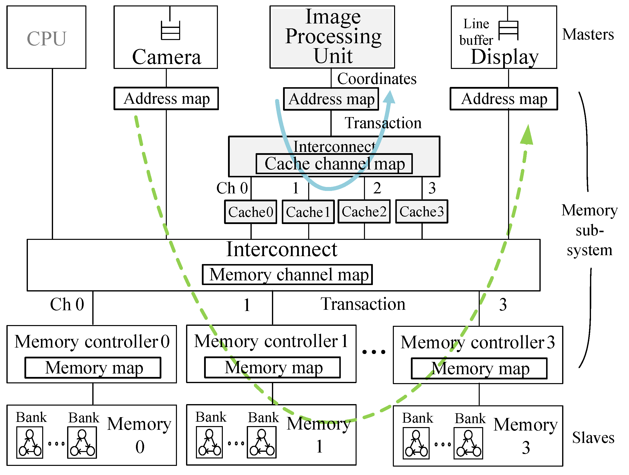
Figure 1. System-on-chip.
Electronics 12 03393 g001
Figure 2. Linear address map (LIAM) in the transaction granularity. The number in the circle indicates the transaction number.
Electronics 12 03393 g002
Figure 3. Cache and memory mapping example.
Electronics 12 03393 g003
Figure 4. Block-level convolution operation.
Electronics 12 03393 g004
Figure 5. Transaction Metric i , j .
Electronics 12 03393 g005
Figure 6. Average metric in LIAM.
Electronics 12 03393 g006
Figure 7. Padded linear address map (pLIAM).
Electronics 12 03393 g007
Figure 8. Pad sizing algorithm.
Electronics 12 03393 g008
Figure 9. Average metric in pLIAM.
Electronics 12 03393 g009
Figure 10. System operation.
Electronics 12 03393 g010
Figure 11. Performance results. The number of cache and memory channels is 4.
Electronics 12 03393 g011
Figure 12. Performance results. The number of cache channel is 4 and the number of memory channels is 2.
Electronics 12 03393 g012
Figure 13. The evaluation on load balancing in the rotated preview (non-cacheable) workload. The lower the deviation between the channels is, the better balanced the load is.
Electronics 12 03393 g013
Figure 14. The evaluation on load balancing in the rotated display (non-cacheable) workload. The lower the deviation between the channels is, the better balanced the load is.
Electronics 12 03393 g014
Figure 15. The evaluation on load balancing in the convolution (cacheable) workload.
Electronics 12 03393 g015
Figure 16. The evaluation on load balancing in the edge detection (cacheable) workload.
Electronics 12 03393 g016
Figure 17. Memory footprint overheads.
Electronics 12 03393 g017
Table 1. Main design parameters.
ParametersDescriptionUnitExample
LineSizeCache line sizebytes64
TranSizeTransaction sizebytes64
MMultiple outstanding count-4
NumCacheChNumber of cache channels-4
NumMemChNumber of memory channels-4
SLSSuper-line size
= LineSize  ×  NumCacheCh
or TranSize  ×  NumMemCh
bytes256
ImgHImage horizontal sizepixels128
ImgVImage vertical sizepixels32
BytePixelByte per pixelbytes4 (RGB)
ImgHBImage horizontal size
= ImgH   ×   BytePixel
bytes512
Table 2. Image size padding examples. An access pattern is non-linear. SLS is 256 bytes. BytePixel is 4 bytes. ImgHB is ImgH × BytePixel. TranSize and LineSize are 64 bytes.
Image Size (Pixels) ImgHB SLS Equation (5)Pad SizePadded Image Size
720 × 48011.25Not met0720 × 480
1280 × 72020Met161296 × 720
1152 × 86418Met161168 × 864
1440 × 108022.5Met161456 × 1080
1680 × 105026.25Not met01680 × 1050
1920 × 108030Met161936 × 1080
2048 × 108032Met162064 × 1080
Table 3. System configuration.
ComponentsItemConfiguration
CacheChannelsConfigurable
Line size64 bytes
Organization16-way set associative
MappingTag, Index, Channel, Offset
Size512 lines
ReplacementLeast Recently Used (LRU)
InterconnectData width128 bits
ArbitrationRound-robin
Transaction size64 bytes
Multiple outstandingMax. 16
Memory ControllerMappingRow, Bank, Col, Channel, Col
Request queue16 entries
Memory (DRAM)ModelDDR3-800
Timingt CL -t RCD -t RP = 5-5-5
ChannelsConfigurable
Schedulingbank-hit first
Banks4
Table 4. Workloads. NC denotes non-cacheable. C denotes cacheable.
WorkloadsTypeComponentOperationAccessPad Size
Camera previewNCCameraWriteRaster scan0
DisplayReadRaster scan0
Image scaling × 1.5NCCameraWriteRaster scan0
ScalerRead, WriteRaster scan0
DisplayReadRaster scan0
Image blendingNCBlenderRead, Read, WriteRaster scan0
Rotated displayNCDisplayReadVertical0 or TranSize
Rotated previewNCCameraWriteVertical0 or TranSize
DisplayReadRaster scan0 or TranSize
Edge detectionCImage processing
unit
Read, Read, WriteBlock0 or LineSize
ConvolutionCImage processing
unit
Read, Read, WriteBlock0 or LineSize
Table 5. Averages of the number of outstanding requests measured during the entire execution time.
WorkloadsLIAMpLIAM
Rotated previewChannel 0:4.0Channel 0:2.68
Channel 1:4.0Channel 1:2.62
Channel 2:4.0Channel 2:2.51
Channel 3:4.0Channel 3:2.61
Rotated displayChannel 0:3.04Channel 0:1.38
Channel 1:3.03Channel 1:1.38
Channel 2:3.03Channel 2:1.38
Channel 3:3.04Channel 3:1.38
ConvolutionCache 0:0.53Cache 0:0.68
Cache 1:0.51Cache 1:0.59
Cache 2:0.49Cache 2:0.61
Cache 3:0.49Cache 3:0.58
Edge detectionCache 0:0.46Cache 0:0.50
Cache 1:0.43Cache 1:0.44
Cache 2:0.41Cache 2:0.43
Cache 3:0.42Cache 3:0.43
Table 6. Standard deviations of the number of outstanding requests measured every 500 cycles. Lower is better.
WorkloadsLIAMpLIAMImprovement (%)
Rotated preview6.92.2667.2
Rotated display5.330.2595.3
Convolution0.590.3639.1
Edge detection0.510.478.8
Disclaimer/Publisher’s Note: The statements, opinions and data contained in all publications are solely those of the individual author(s) and contributor(s) and not of MDPI and/or the editor(s). MDPI and/or the editor(s) disclaim responsibility for any injury to people or property resulting from any ideas, methods, instructions or products referred to in the content.