Communication

Research on High-Dose-Rate Transient Ionizing Radiation Effect in Nano-Scale FDSOI Flip-Flops

1
Beijing Microelectronics Technology Institute, Beijing 100076, China
2
Laboratory of Science and Technology on Radiation-Hardened Integrated Circuits in CASC, Beijing 100076, China
3
China Academy of Aerospace Electronics Technology, Beijing 100094, China
*
Author to whom correspondence should be addressed.
Electronics 2023, 12(14), 3149; https://doi.org/10.3390/electronics12143149
Submission received: 9 June 2023 / Revised: 6 July 2023 / Accepted: 7 July 2023 / Published: 20 July 2023
(This article belongs to the Special Issue Radiation Effects of Advanced Electronic Devices and Circuits)

Abstract

:
This paper presents an experimental study on the high-dose-rate transient ionizing radiation response and influencing factors of a Nano-Scale Fully Depleted Silicon-On-Insulator (FDSOI) D flip-flops (DFFs) circuit. Results indicate that data errors occur in DFFs at the lowest dose rate of 4.70 × 10¹¹ rad(Si)/s in experiments, and the number of data errors shows a nonlinear increasing trend with the increase in dose rate and supply voltage. Three-dimensional technology computer-aided design (TCAD) simulations were conducted to analyze the transient photocurrent and charge collection mechanism at advanced process. The simulation results indicated that the charge collection efficiency is heightened with an increase in supply voltage, resulting in the higher photocurrent. This plays a major role in the process of charge collection for Ultra-Thin Body and Buried oxide (UTBB) FDSOI technology. The investigation into the high-dose-rate transient ionizing radiation effect (HDR-TIRE) in Nano-Scale FDSOI DFFs will aid in the assessment and application of advanced integrated circuits in aerospace.

1. Introduction

Exposure to various radiation environments may result in diverse radiation effects on Integrated Circuits (ICs), such as high-dose-rate transient ionizing radiation effect (HDR-TIRE), total ionizing dose effect (TID) and single-event effect (SEE). HDR-TIRE is a phenomenon in which circuits experience signal upset and strong disturbance when exposed to high-dose-rate radiation environments. This effect is primarily caused by the generation of transient photocurrents in semiconductor devices due to ionizing effects. The stability of the supply voltage is crucial for the proper functioning of ICs. Unfortunately, HDR-TIRE causes significant disruptions to the supply voltage, which directly affects the normal operation of circuits [1,2,3,4,5]. Currently, experimental studies of HDR-TIRE depend on large ground-based devices to build up the radiation environment, while relevant research is carried out by using “Qiangguang-I” accelerator.
As the feature size of Nano-Scale ICs continues to scale down, short-channel effects (SCEs) limit the performance of traditional bulk planar technology. To extend CMOS scaling beyond the sub-28 nm node, Fin Field-Effect Transistor (FinFET) and FDSOI technology routes have been proposed. Nano-Scale FDSOI technology has overcome the performance of traditional planar bulk transistors due to improved electrostatic control, and it is scalable according to Moore’s Law. In addition, it provides best the performance-power tradeoffs using the body biasing [6]. Moreover, FDSOI has great potential for military and space applications.
SOI, as a modern type of semiconductor device structure, has also attracted considerable attention in the field of radiation hardening [7,8,9,10]. To achieve a complete dielectric isolation structure, a thin layer of SiO2 is inserted into the substrate of SOI devices, which eliminates the latch-up effect commonly found in traditional bulk devices [11]. Additionally, the buried oxide (BOX) layer prevents a significant amount of charge generated in the substrate from being collected by the top silicon film, leading to a lower intensity of photocurrent generated by SOI circuits compared to bulk circuits in a high dose rate irradiation environment [12,13,14]. A previous study showed that SOI presents a bipolar parasitic transistor, which may amplify the charge injected by irradiation [15]. Under the same process conditions, the tolerance to HDR-TIRE of an SOI device is substantially improved [16]. SOI devices can be divided into PDSOI (Partially Depleted) and FDSOI (Fully Depleted), in which the FDSOI structure gains high tolerance against radiation [17]. The structure comparison between FDSOI and a planar bulk device is shown in Figure 1.
A study has investigated the HDR-TIRE of SOI CMOS RF ICs [18]. A radiation-hardened FPGA chip based on a 0.5 μm SOI process has been shown to tolerate a dose rate of over 1.5 × 10¹¹ rad(Si)/s [19]. For a radiation-hardened SRAM chip with a 0.8 μm SOI process, although the stored data remained intact and the read/write function worked normally after being exposed to a dose rate of 2.45 × 10¹¹ rad(Si)/s, there was an increase in current after irradiation from the experiment results [20]. However, related research into advanced integrated circuits based on Ultra-Thin Body and Buried oxide (UTBB) FDSOI technology has not been reported.
Flip-flops are one of the fundamental and widely used components in digital circuits. Therefore, it is essential to discover the radiation response of flip-flops. This paper focuses on an experimental and simulation study to investigate the impact of supply voltage and dose rate on the high-dose-rate transient ionizing radiation response of FDSOI-based D Flip-Flops (DFFs). In the following Section 2 and Section 3, the test circuit based on Nano-Scale FDSOI and experiment setups is described. Additionally, experimental and simulation results are discussed in Section 4. Finally, the conclusion of the analyzed data is provided in Section 5.

2. Circuit Samples

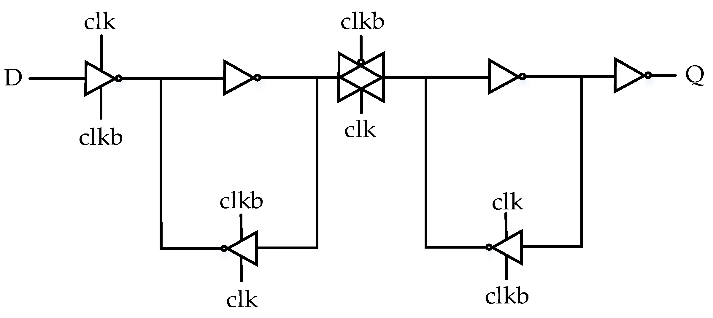
The test sample was a customized Nano-Scale UTBB FDSOI DFFs circuit, which was developed to test and verify the radiation tolerance performance of FDSOI technology. Figure 2 shows the structure schematic of conventional DFF [21]; it is composed of two latches, each designed with back-to-back connect inverters, where D is the input, clk is the clock signal, and Q is the output.

3. Radiation Experiments

The high-dose-rate transient ionizing radiation experiments were carried on the “Qiangguang-I” accelerator at Northwest Institute of Nuclear Technology. This accelerator is capable of simulating a variety of pulsed radiation environments formed by nuclear explosions. Experiments were performed by simultaneously bombarding multiple samples. In order to shield electromagnetic interference, the devices under the test board and configuration board were placed in aluminum boxes. The dose rate values required were obtained by placing the sample at a certain position from the gamma ray radiation source. Additionally, two power supply voltages (0.8 V and 0.88 V) were set up, respectively, in this experiment for observing the radiation characteristics of supply voltage effect.

4. Experimental Analysis and Discussion

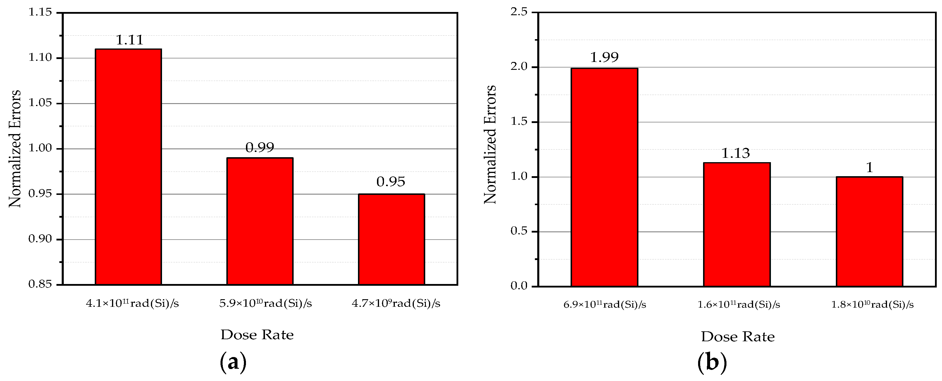
The relationship between data errors of FFs and dose rate values for different supply voltages is represented in Figure 3, where the number of data errors is normalized to the value at 0.88 V supply voltage and 1.80 × 10¹⁰ rad(Si)/s dose rate. The supply voltage was set to 0.8 V in Figure 3a, and it can be calculated that the normalized error increased by 4.2% as the dose rate was raised from 4.70 × 10⁹ rad(Si)/s to 5.90 × 10¹⁰ rad(Si)/s; the dose rate is increased by a factor of 12.6. It increased by 16.8% as the dose rate was raised from 4.70 × 10⁹ rad(Si)/s to 4.10 × 10¹¹ rad(Si)/s, and the dose rate increased by a factor of 87.2. Additionally, the normalized error was increased by 12.1%, with the dose rate increasing by a factor of 6.9 from 5.90 × 10¹⁰ rad(Si)/s to 4.10 × 10¹¹ rad(Si)/s. When the supply voltage was 0.88 V, as shown in Figure 3b, the normalized error was raised by 13.0% and 99.0% with the dose rate increased from 1.80 × 10¹⁰ rad(Si)/s to 1.60 × 10¹¹ rad(Si)/s and 1.80 × 10¹⁰ rad(Si)/s to 6.90 × 10¹¹ rad(Si)/s, respectively; the dose rates increased by a factor of 8.9 and 38.3. Test results have confirmed a nonlinear increase in data errors induced by transient ionizing radiation as the dose rate increased. It is noted that though the dose rate value could be roughly expected according to the distance from the radiation source, the same order of magnitude of dose rate values could not be completely equivalent during multiple trials.
Supply voltage acted as a global influence factor on the high-dose-rate transient ionizing radiation response in the circuit. As illustrated in Figure 4, the number of the normalized error was lower for the 0.8 V and 4.10 × 10¹¹ rad(Si)/s combination than the 0.88 V and 1.60 × 10¹¹ rad(Si)/s combination, which indicates that even with a lower dose rate a higher supply voltage results in a higher number of errors in DFFs.
The impact of the supply voltage on the high-dose-rate transient ionizing radiation response of FDSOI circuits is closely related to the circuit structure and power supply network. This complexity is reflected in the behavior of the electron-hole pairs. Some work has been based on circuit level simulation [22], but this is not adequate for research on the microphysical mechanism. Therefore, this paper presents TCAD simulation in order to analyze the HDR-TIRE on Nano-Scale FDSOI devices for different supply voltages. The width of the transistor was 324 nm and 396 nm, corresponding to NMOS and PMOS, respectively. The buried oxide layer thickness was 20 nm. The top silicon film thickness was 6 nm. Three-dimensional TCAD models were developed using the Synopsys Sentaurus suit of TCAD tools.
The initial device models of NMOS and PMOS were established and the electrical characteristic curves were simulated. The gate voltage was swept from 0 V to 0.8 V for NMOS and from −0.8 V to 0 V for PMOS. Additionally, the electrical characteristic curves of NMOS and PMOS in the SPICE model were obtained. The results of the electrical characteristics calibration are shown in Figure 5. It can be seen that the electrical characteristic curves of the two models could be matched nicely with an average error of less than 5%, indicating that the established FDSOI device models can be used for HDR-TIRE simulations.
As depicted in Figure 6, the 3D model of the Nano-Scale FDSOI inverter was established based on NMOS and PMOS devices. The logic function of the inverter was correct and the inverter gate switching time was less than 60 ps. Therefore, it could be operated normally at the frequency of 15 GHz.
Supply voltage is a key factor for both SEE [23] and HDR-TIRE [24]. As ICs technology advances, Moore’s law describes ICs development accurately, namely, performance improvement and power consumption reduction. For Nano-Scale FDSOI, the standard core supply voltage has been reduced to 0.8 V. Additionally, since the thickness of the top silicon film is on the order of a few nanometers, the mechanism of HDR-TIRE for different supply voltages is quite complicated. Therefore, this paper presents a simulation study of the FDSOI inverter in order to explore the effect of power supply voltage on high-dose-rate transient ionizing radiation response and charge collection mechanism. The simulations were carried out for two supply voltages (0.8 V, 1.2 V) and two dose rates (1 × 10¹² rad(Si)/s, 1 × 10¹¹ rad(Si)/s).
HDR-TIRE results in the appearance of photocurrent pulses in the device. To facilitate the observation of the leakage current variation, the ΔIpeak for different supply voltages is compared in Figure 7a. ΔIpeak is defined as the difference between photocurrent peak and initial leakage current since raising the supply voltage can increase the initial static leakage current of the device. The ΔIpeak was normalized with a 0.8 V supply voltage and a dose rate of 1 × 10¹² rad(Si)/s condition, which was 8.24 × 10⁻⁸ A. It can be illustrated that an increase in supply voltage leads to an increase in ΔIpeak, as the dose rate is fixed. For instance, the ΔIpeak increased by a factor of 5.5 when the supply voltage was increased from 0.8 V to 1.2 V at the dose rate of 1 × 10¹² rad(Si)/s. And the ΔIpeak at a dose rate of 1 × 10¹² rad(Si)/s was 5× larger than that of 1 × 10¹¹ rad(Si)/s for the 0.8 V supply voltage. Moreover, compared with the 0.8 V@1 × 10¹² rad(Si)/s case in Figure 7a, the supply voltage increased to 1.2 V, although the dose rate reduced to 1 × 10¹¹ rad(Si)/s. The ΔIpeak increased by a factor of 2.2, which indicates the dominant effect of supply voltage on the photocurrent.
Coupled with the photocurrent integral, the charge collection (Qcol) was obtained and the comparison is shown in Figure 7b. It can be concluded that the supply voltage increased from 0.8 V to 1.2 V, and Qcol increased by a factor of 13.8 at a dose rate of 1 × 10¹² rad(Si)/s and increased by a factor of 30.3 at a dose rate of 1 × 10¹¹ rad(Si)/s. This suggests that the increase in supply voltage leads to a broadening of the photocurrent pulse width, which results in a greater increase in Qcol than ΔIpeak.
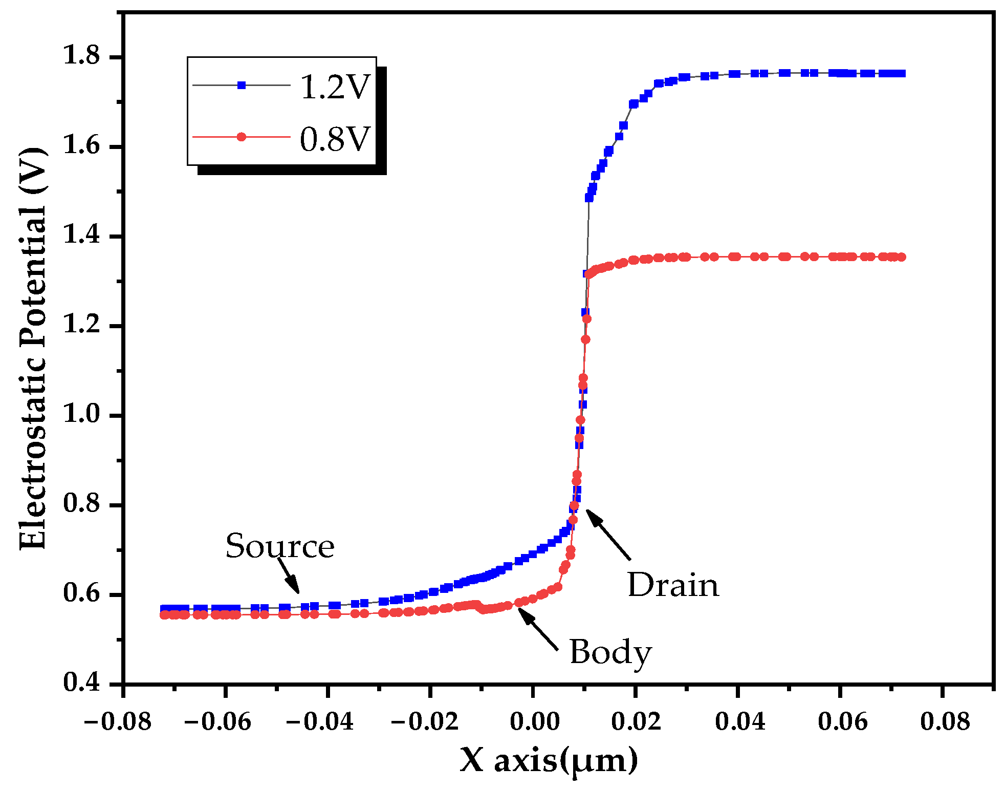
Increasing the supply voltage resulted in an enhanced internal electric field, which led to an increase in the amount of charge collection and a rise in the body potential, as shown in Figure 8. As a result, the parasitic bipolar amplification became more efficient, leading to an increase in the photocurrent peak. It should be noted that increasing the supply voltage can contribute to the increase in the restore current and the competitive factor may mitigate the photocurrent, while from the simulation results the bipolar effect is the dominant mechanism.

5. Conclusions

In order to investigate the high-dose-rate transient ionizing radiation response of a Nano-Scale FDSOI circuit with an ultra-thin top silicon film under different dose rates and supply voltages, this paper presents an experimental study of a Nano-Scale FDSOI DFFs circuit. The results indicated that HDR-TIRE causes a data error at the dose rate of 4.70 × 10⁹ rad(Si)/s, and the number of errors increases nonlinearly with the increase in dose rate value.
For the 0.8 V supply voltage, the dose rate increased 6.9-fold and 12.6-fold, from 5.9 × 10¹⁰ rad(Si)/s to 4.1 × 10¹¹ rad(Si)/s and 4.7 × 10⁹ rad(Si)/s to 5.9 × 10¹⁰ rad(Si)/s; the normalized error increased by 12.1% and 4.2%, respectively. An increase in the dose rate led to a higher number of generated electron-hole pairs. This impacted the electrostatic potential and charge collection mechanisms such as drift process and parasitic bipolar amplification. There was a synergistic effect, resulting in the nonlinear relationship between dose rate value and data errors. The experimental results showed that even with a lower dose rate, a higher supply voltage results in a higher number of data errors in DFFs. Three-dimensional TCAD simulations of the devices were performed. It was found that the number of charges collected increases with the increase in supply voltage for the enhancement of the parasitic bipolar amplification effect in the Nano-Scale FDSOI device. Understanding the high-dose-rate transient ionizing radiation response of the Nano-Scale FDSOI circuit and the impact of factors such as supply voltage is important when considering radiation-hardening techniques.

Author Contributions

Conceptualization and methodology, T.L.; validation, L.W.; formal analysis, T.L.; writing—original draft preparation, T.L.; writing—review and editing, Y.B. and L.S.; visualization, J.Y., C.Y. and C.G.; supervision, Y.Z.; project administration, Y.Z. All authors have read and agreed to the published version of the manuscript.

Funding

This research was supported by the Qian Xuesen Youth Innovation Fund. NO. 2021.01.

Data Availability Statement

Not applicable.

Acknowledgments

The authors would like to thank Chenhui Wang at the Northwest Institute of Nuclear Technology for the help and support with the chip test.

Conflicts of Interest

The authors declare no conflict of interest.

References

  1. Hu, C.; He, C. Numerical Simulation of Neutron Irradiation in Ultra-Deep Submicron SOI NMOSFETs. At. Energy Sci. Technol. 2011, 45, 456–460. [Google Scholar]
  2. Xue, H.; Zhang, M. Numerical Simulation of Transient Dose Rate Effects in NMOS Devices with Deep Submicron SOI process. Appl. Electron. Technol. 2019, 45, 59–61. [Google Scholar]
  3. Niu, Z.; Tu, Y. Research on Neutron Irradiation Effect of Computer Based on DSP. In Proceedings of the 10th Annual National Conference on Radiation Resistant Electronics and Electromagnetic Pulse, Shenyang, China, 1 July 2009; pp. 97–102. [Google Scholar]
  4. Liu, W. Radiation Effects of Silicon Semiconductor Devices and Reinforcement Techniques, 1st ed.; Beijing Science Press: Beijing, China, 2013; pp. 132–136. [Google Scholar]
  5. Ellis, T.D.; Kim, Y.D. Use of a Pulsed Laser as an Aid to Transient Upset Testing of 12L LSI Microcircuits. IEEE Trans. Nucl. Sci. 1978, 25, 1489–1493. [Google Scholar] [CrossRef]
  6. Weber, O. FDSOI vs FinFET: Differentiating Device Features for Ultra Low Power & IoT applications. In Proceedings of the 2017 IEEE International Conference on IC Design and Technology (ICICDT), Austin, TX, USA, 23–25 May 2017; pp. 1–3. [Google Scholar]
  7. Luo, H. SOI Devices and Applications. Electron. Packag. 2007, 7, 41–45. [Google Scholar]
  8. Perin, L.; Pereira, A. SOI Stacked Transistors Tolerance to Single-Event Effects. IEEE Trans. Device Mater. Reliab. 2019, 19, 393–401. [Google Scholar] [CrossRef]
  9. Heidel, A. Single-Event Upsets and Multiple-Bit Upsets on a 45 nm SOI SRAM. IEEE Trans. Nucl. Sci. 2009, 56, 3499–3504. [Google Scholar] [CrossRef]
  10. Elesin, V.; Nazarova, G. Investigation of the Possibility to Develop Radiation-Hardness LSIs for Navigational Purposes According to the 0.35-μm Domestic CMOS SOI Technology. Russ. Microelectron. 2012, 41, 266–277. [Google Scholar] [CrossRef]
  11. Zhang, Z.; Liu, J. Investigation of Threshold Ion Range for Accurate Single Event Upset Measurements in Both SOI and Bulk Technologies. IEEE Trans. Nucl. Sci. 2014, 61, 1459–1467. [Google Scholar] [CrossRef]
  12. Raine, M.; Gaillardin, M. Experimental Evidence of Large Dispersion of Deposited Energy in Thin Active Layer Devices. IEEE Trans. Nucl. Sci. 2011, 58, 2664–2672. [Google Scholar] [CrossRef]
  13. Wirth, J.; Rogers, S. The Transient Response of Transistors and Diodes to Ionizing Radiation. IEEE Trans. Nucl. Sci. 1964, 11, 24–38. [Google Scholar] [CrossRef]
  14. Palkuti, L.; Alles, M. The Role of Radiation Effects in SOI Technology Development. In Proceedings of the 2014 SOI-3D-Subthreshold Microelectronics Technology Unified Conference (S3S), Millbrae, CA, USA, 6–9 October 2014; pp. 1–2. [Google Scholar]
  15. Schwank, J.; Ferlet, V. Radiation Effects in SOI Technologies. IEEE Trans. Nucl. Sci. 2003, 50, 522–538. [Google Scholar] [CrossRef]
  16. Zhang, Z.; Zou, S. Radiation Hardening Technology of SOI Materials and Devices. Chin. Sci. Bull. 2017, 62, 1004–1017. [Google Scholar] [CrossRef] [Green Version]
  17. Ferlet, V.; Gasiot, G. Insights on the Transient Response of Fully and Partially Depleted SOI Technologies Under Heavy-ion and Dose-Rate Irradiations. IEEE Trans. Nucl. Sci. 2002, 49, 2948–2956. [Google Scholar] [CrossRef]
  18. Nazarova, G.; Elesin, V. Long-Term Transient Radiation Effects in SOI CMOS RF ICs. In Proceedings of the 2015 15th European Conference on Radiation and Its Effects on Components and Systems (RADECS), Moscow, Russia, 14–18 September 2015; pp. 1–4. [Google Scholar]
  19. Wu, L.; Han, X. Radiation-hardened SOI Process Design and FPGA. Inf. Electron. Eng. 2012, 10, 627–632. [Google Scholar]
  20. Zhao, K.; Liu, Z. Resist Radiation 128 KB PDSO1 Static Random Access Memory. J. Semicond. 2007, 7, 1139–1143. [Google Scholar]
  21. Ball, D.; Alles, M. The Impact of Charge Collection Volume and Parasitic Capacitance on SEUs in SOI- and Bulk-FinFET D Flip-Flops. IEEE Trans. Nucl. Sci. 2018, 65, 326–330. [Google Scholar] [CrossRef]
  22. Liu, H.; Golke, K. A New Dose Rate Model for SOI MOSFETs and Its Implementation in SPICE. In Proceedings of the 2005 IEEE International SOI Conference Proceedings, Honolulu, HI, USA, 3–6 October 2005; pp. 112–113. [Google Scholar]
  23. Kauppila, J.; Kay, W. Single-Event Upset Characterization Across Temperature and Supply Voltage for a 20-nm Bulk Planar CMOS Technology. IEEE Trans. Nucl. Sci. 2015, 62, 2613–2619. [Google Scholar] [CrossRef]
  24. Li, T.; Zhao, Y. Investigation on Transient Ionizing Radiation Effects in a 4-Mb SRAM with Dual Supply Voltages. IEEE Trans. Nucl. Sci. 2022, 69, 340–348. [Google Scholar] [CrossRef]
Figure 1. Schematic diagram of the device structure of bulk and FDSOI processes.
Electronics 12 03149 g001
Figure 2. Schematic of Conventional DFF.
Electronics 12 03149 g002
Figure 3. The relationship between normalized data errors and dose rate for different supply voltages. (a) Supply voltage is 0.8 V; (b) supply voltage is 0.88 V.
Electronics 12 03149 g003
Figure 4. Comparison of normalized errors with different dose rates and supply voltages. The unit of DoseRate is 1 × 10¹¹ rad(Si)/s.
Electronics 12 03149 g004
Figure 5. FDSOI device model calibration results. (a) NMOS; (b) PMOS.
Electronics 12 03149 g005
Figure 6. TCAD model of nano-scale FDSOI inverter.
Electronics 12 03149 g006
Figure 7. Comparison of normalized photocurrent peak and charge collection with different supply voltages and dose rates of inverter. (a) ΔIpeak; (b) Qcol.
Electronics 12 03149 g007
Figure 8. Effect of supply voltage on electrostatic potential distribution. The dose rate is 1 × 10¹² rad(Si)/s.
Electronics 12 03149 g008
Disclaimer/Publisher’s Note: The statements, opinions and data contained in all publications are solely those of the individual author(s) and contributor(s) and not of MDPI and/or the editor(s). MDPI and/or the editor(s) disclaim responsibility for any injury to people or property resulting from any ideas, methods, instructions or products referred to in the content.