1. Introduction
Propulsion systems such as those found in automobiles, ships, and aircraft have conventionally used fossil fuels and an internal combustion engine. Recently, they have begun to be converted into electric propulsion systems based on electric powertrains composed of a battery, electric motor, and inverter [
1,
2,
3,
4,
5,
6]. The demand for batteries has increased, especially among electric powertrain systems, and the amount of research on battery simulators and DC power supplies that can simulate the DC voltage of a battery has also increased [
7,
8,
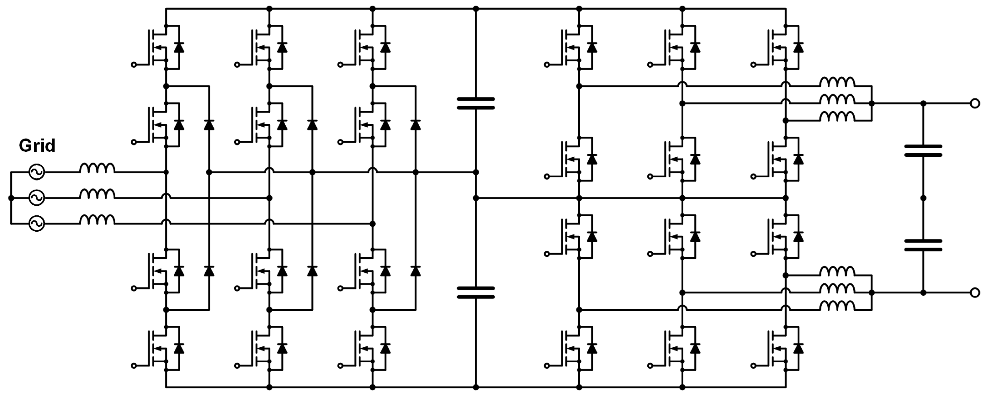
9]. The battery simulator and DC power supply are generally applied with a two-stage power conversion system consisting of two different power conversion systems. The two-stage power conversion system consists of a grid-connected PWM converter and DC–DC converter, as shown in
Figure 1 [
10,
11]. The PWM converter converts the three-phase AC voltage of the grid into DC voltage, and the DC–DC converter outputs a wide range of DC voltages from the limited DC voltage of the PWM converter and supports the fast response of voltage control.
The output voltage of a battery is basically DC voltage that does not include ripple, and the battery simulator that simulates the battery voltage and DC power supply also needs to minimize the ripple of the output voltage. Therefore, a DC–DC converter is configured in three levels and in parallel, as shown in
Figure 1, and each leg of the DC–DC converter is interleaved to reduce the output current and voltage ripple [
12,
13]. However, the ripple of the current flowing through each inductor constituting the DC–DC converter increases due to the circulating current, and the inductor current ripple causes problems such as system loss and inductor saturation [
14,
15]. The method for reducing the circulating current that causes inductor current ripple in the interleaved DC–DC converter has been studied previously [
14,
15,
16,
17]. In [
14,
15], a coupled inductor that could suppress the circulating current was used instead of a general inductor. Although the method was effective at reducing the inductor current ripple, it was expensive, and the coupled inductor required a complicated design to obtain the required current ripple. In [
16], since the top and bottom switches were interleaved and each leg was operated without interleaved switching, the output voltage ripple and inductor current ripple were reduced compared to the two-level system. However, the output voltage ripple fell compared to that of the overall interleaved operation, which was a problem. In [
17], the converter was controlled by zero current transition through an additional inductor, and the inductor current ripple was also reduced. However, there was a disadvantage in that the inductor current of each leg increased because each leg was controlled alternately without simultaneously controlling the output current.
This paper analyzes the inductor current ripple and output current ripple in a three-parallel three-level DC–DC converter. Additionally, the relationship between the output voltage, duty ratio, and inductor current ripple of the DC–DC converter is analyzed. To minimize the inductor current ripple of the DC–DC converter, we propose a method to optimally control the DC link voltage through the PWM converter in the two-stage power conversion system. In the proposed method, no additional hardware or complex control algorithms are required, and only the DC link voltage reference of the PWM converter is changed, without modifying the control algorithm of the PWM converter and DC–DC converter.
Since most existing methods for reducing inductor current ripple have been studied only under the condition that the DC–DC converter is operated alone, an addition or change of hardware such as the coupled inductor is required, and most existing papers have only discussed the design of the coupled inductor. However, the method proposed in this paper intends to reduce the inductor current ripple of the DC–DC converter under the condition that the PWM converter and DC–DC converter constituting the two-stage power conversion system are operated together. In addition, the effect of reducing the inductor current ripple can be further improved, or the size of the inductor can be further reduced, since the proposed method can be applied in conjunction with most existing methods. To verify the feasibility of the proposed method, the simulation and experimental results for the two-stage power conversion system under various operating conditions are presented.
2. Inductor Current Ripple of the Three-Parallel Three-Level DC–DC Converter
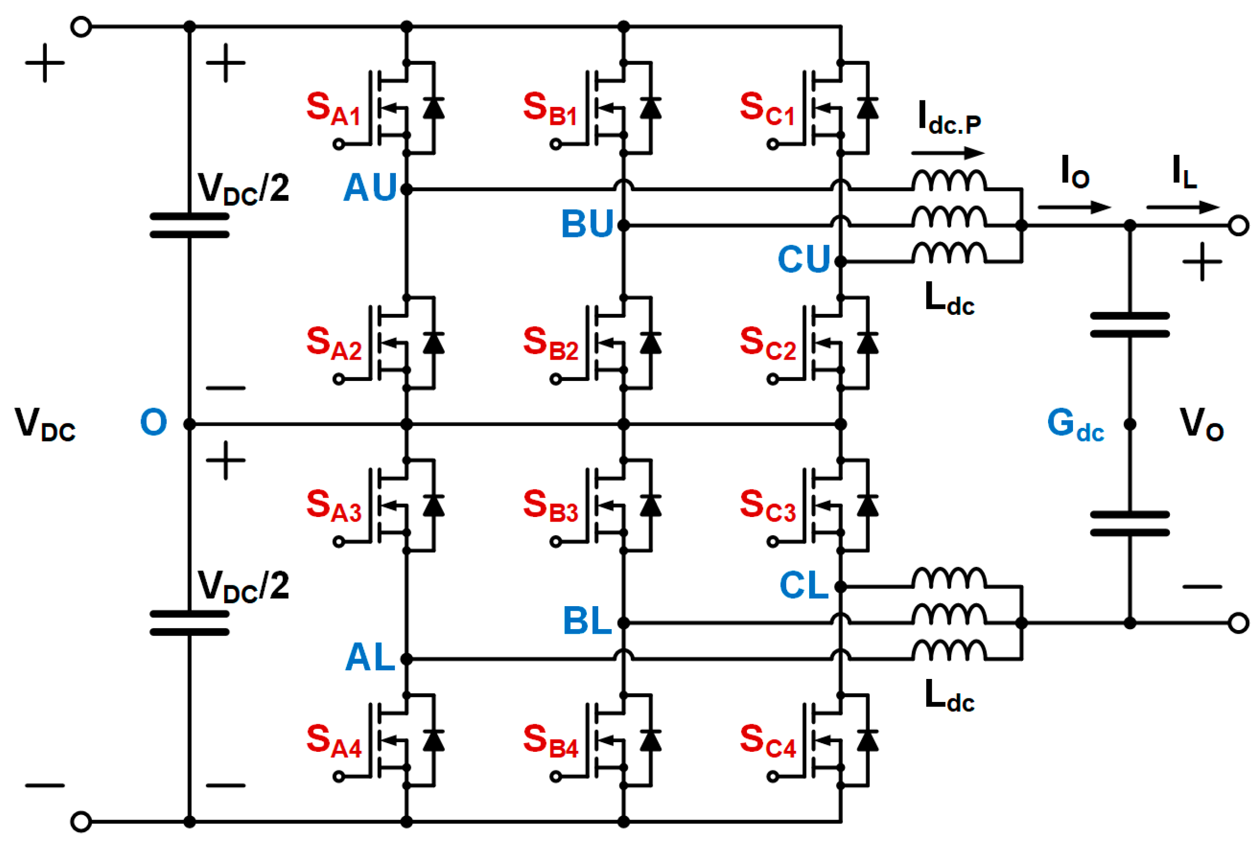
The two-stage power conversion system of this paper consists of a three-phase three-level NPC converter and a three-parallel three-level DC–DC converter [
18,
19]. The three-parallel three-level DC–DC converter is composed of three three-level DC–DC converters, and
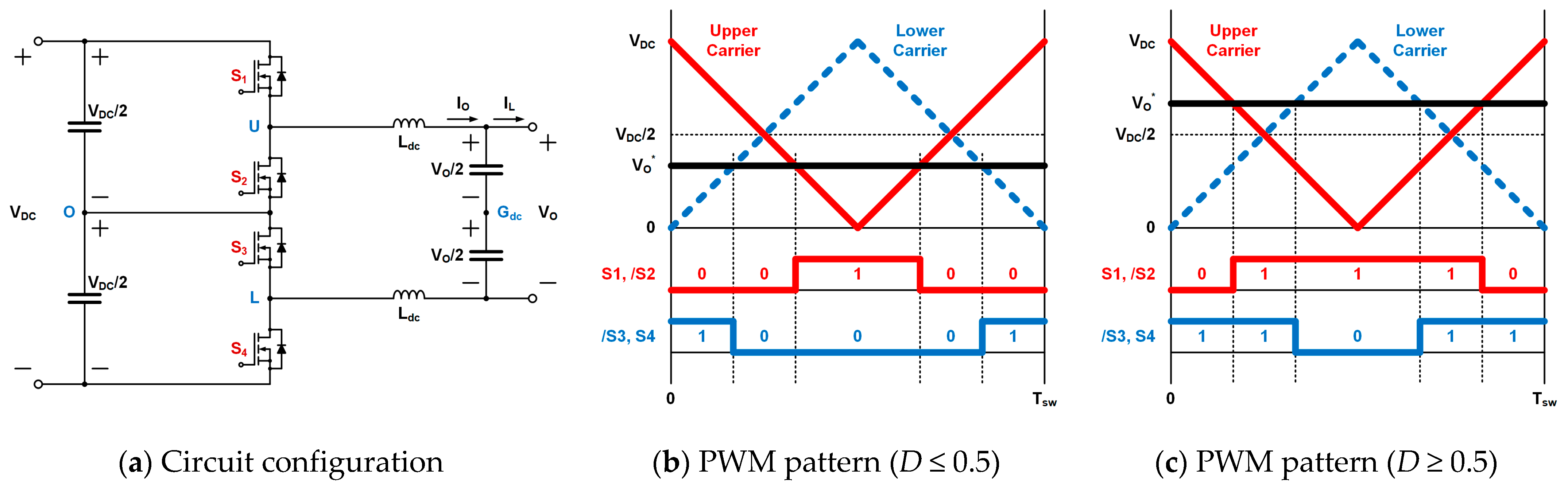
Figure 2 shows the circuit configuration of this three-level DC–DC converter. The basic circuit, defined as a leg or pole in the three-level DC–DC converter, is configured by connecting four switching devices (S
1, S
2, S
3, and S
4) in series. Switches S
1 and S
2 are switched complementarily, and switches S
3 and S
4 are switched complementarily. The node between switches S
2 and S
3 is connected to a DC link capacitor, and the upper output node (U) between switches S
1 and S
2 and the lower output node (L) between switches S
3 and S
4 are connected to an output capacitor through a DC inductor
Ldc.
The PWM for controlling the three-level DC–DC converter is determined by comparing the output voltage command
VO* with the triangular carrier, as shown in
Figure 2b,c. The states of the upper switches (S
1 and S
2) and lower switches (S
3 and S
4) are determined by the upper carrier and lower carrier, respectively. If the output voltage command is greater than the upper carrier, the topmost switch, S
1, is turned on; if the output voltage command is greater than the lower carrier, the bottommost switch, S
4, is turned on. The triangular carriers have a phase difference of 180° from each other, and so does the PWM of the upper and lower switches. The ratio of the time when switch S
1 or S
4 is turned on to the switching period
Tsw of the DC–DC converter is defined as the output voltage duty ratio
D, which can be expressed as a ratio of the output voltage command to the DC link voltage
VDC, as shown in Equation (1).
The voltage applied to the upper DC inductor is expressed as the relationship between the upper output node voltage
VUO, the common mode voltage
VGdcO, and the output voltage
VO, as shown in Equation (2). The voltage applied to the lower DC inductor is expressed as shown in Equation (3). The inductor current
Idc is rearranged from Equations (2) and (3) to Equation (4), and Equation (4) is rearranged to Equation (5) according to the switching state of the three-level DC–DC converter and Equation (1).
x and
y represent the switching states of the topmost switch S
1 and bottommost switch S
4, respectively; they are 1 when the switch is turned on and 0 when the switch is turned off.
The parallel configuration of the DC–DC converter can increase the output current of the system and has the advantage of improving the performance of the system. The three-parallel three-level DC–DC converter consists of three three-level DC–DC converter legs in parallel, as shown in
Figure 3. Each leg is composed of four switches (S
P1, S
P2, S
P3, and S
P4 (P = A, B, C)), shares the DC link, and the upper output node (PU) and lower output node (PL) are connected to the output capacitor through the DC inductor. The output current
IO of the three-parallel three-level DC–DC converter is expressed by Equation (6), which is the sum of the DC inductor currents
Idc.P of each leg. By rearranging Equations (2), (3), and (6), the output current for the upper and lower DC inductors can be expressed by Equations (7) and (8), respectively.
where
VUO.P is the upper node output voltage of each leg and
VLO.P is the lower node output of each leg.
The output current is rearranged from Equations (7) and (8) to Equation (9), and Equation (9) is rearranged to Equation (10) through the switching state of the three-parallel three-level DC–DC converter and Equation (1).
i represents the number of turned-on switches among the three top switches (S
P1) and
j represents the number of turned-on switches among the three bottom switches (S
P4).
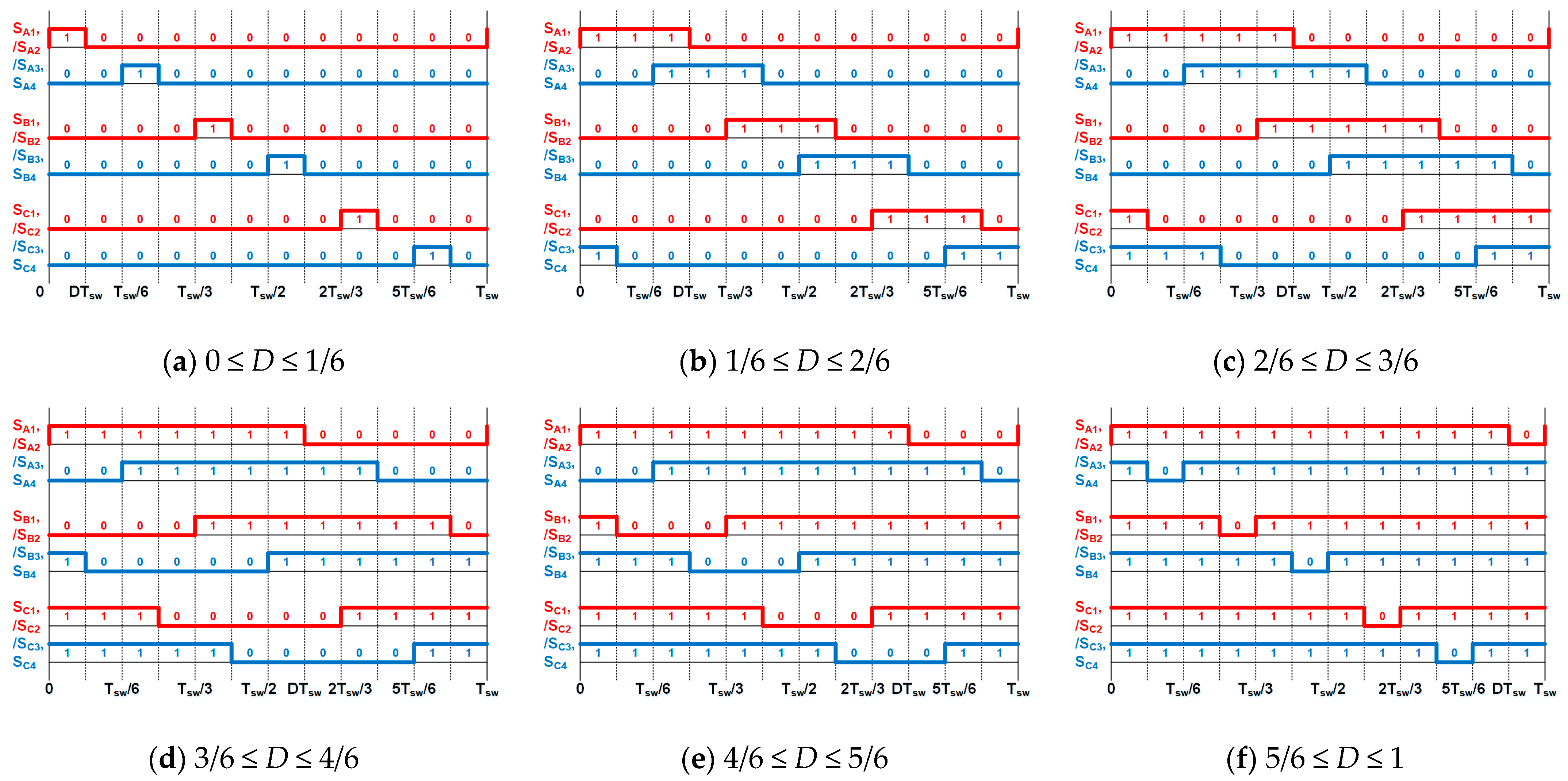
The N-type interleaved PWM is a general PWM method for the three-parallel three-level DC–DC converter [
14]. Based on the uppermost switch S
A1 of the A-leg, the N-type interleaved PWM is turned on in the order of switches S
A1, S
A4, S
B1, S
B4, S
C1, S
C4, and has an interleaved angle of 60°.
Figure 4 shows the switching state according to the output voltage duty ratio during the switching period. It is divided into six regions (0~1/6, 1/6~2/6, 2/6~3/6, 3/6~4/6, 4/6~5/6, and 5/6~1), depending on the output voltage duty ratio and the number of switches that are turned on together. In
Figure 4, the N-type interleaved PWM is composed of 12 switching states during the switching period. Since Equation (5) and Equation (10) represent the change in the inductor current and output current according to the switching state of the three-parallel three-level DC–DC converter, respectively, the DC inductor current ripple Δ
Idc.P and output current ripple Δ
IO according to each region can be represented as shown in Equation (11), by combining Equation (5), Equation (10), and the time when each switching state is applied. Each current ripple is affected by the output voltage duty ratio, the inductance of the DC inductor, the switching frequency
fsw, and the DC link voltage.
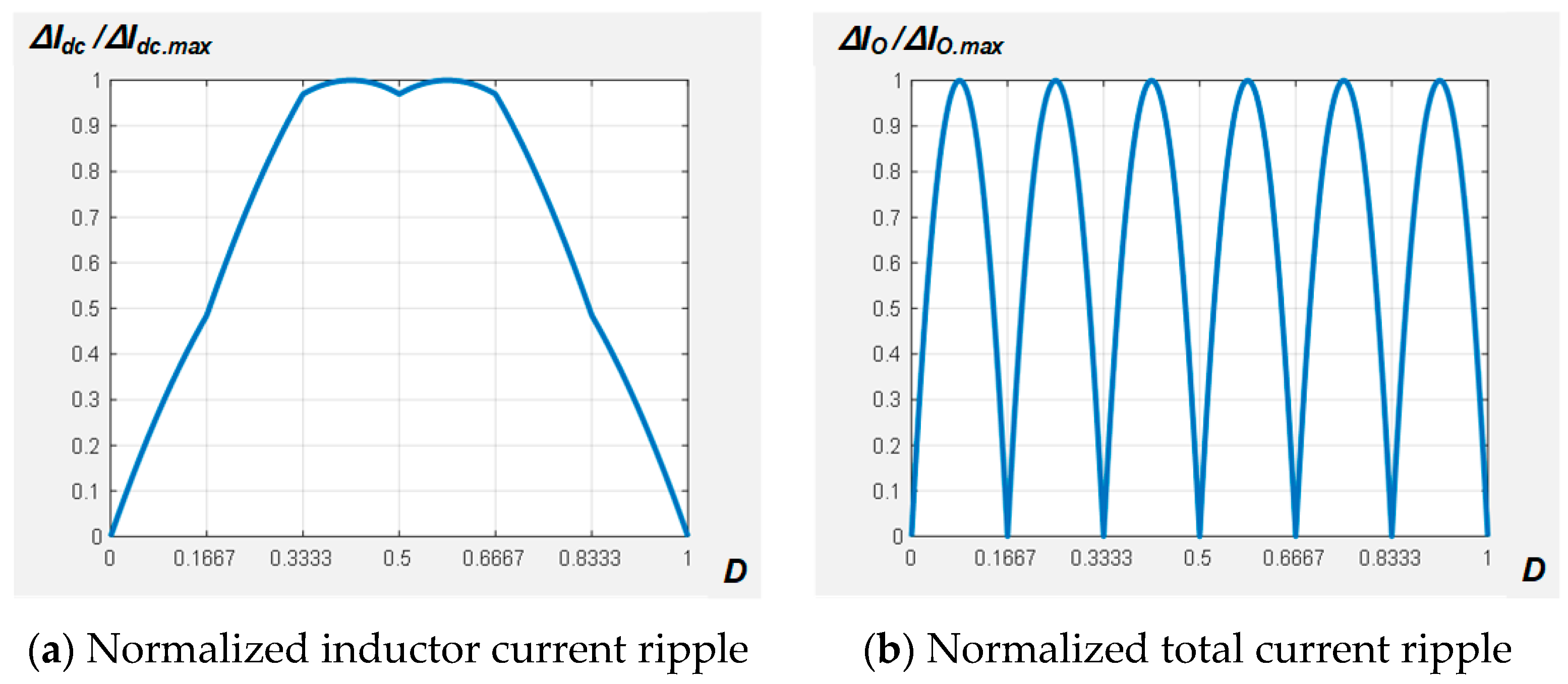
From Equation (11), the normalized DC inductor current ripple according to the duty ratio is shown in
Figure 5a. When the duty ratio is 5/12 or 7/12, the DC inductor current ripple reaches its maximum, as shown in Equation (12), and the DC inductor current ripple in
Figure 5a is normalized based on Equation (12). In addition, the normalized output current ripple according to the duty ratio is shown in
Figure 5b. When the duty ratio is 1/12, 3/12, 5/12, 7/12, 9/12, or 11/12, the output current ripple shown in
Figure 5b is maximized, as shown in Equation (13), and the output current ripple shown in
Figure 5b is normalized based on Equation (13).
The performance of the two-stage power conversion system can be improved by minimizing the output current ripple caused by the N-type interleaved PWM, but the maximum value of the inductor current ripple is 11 times larger than the maximum value of the output ripple, and the inductor current ripple generates power loss in the system and the saturation of the DC inductor.
3. Proposed Current Ripple Reduction Method
Among the parameters that determine the DC inductor current ripple and output current ripple of the three-parallel three-level DC–DC converter in Equation (11), the inductance of the DC inductor and switching frequency are those determined at the stage of the system design and manufacture. Thus, the inductance and frequency are difficult to change and their range is limited during the control of the system. However, since the output voltage duty ratio and DC link voltage can be controlled in real time through the existing PI controller applied in the DC–DC converter and PWM converter, the output voltage duty ratio and DC link voltage are required to reduce the DC inductor current ripple and output current ripple.
In addition, since the two-stage power conversion system in this paper is applied to applications such as a battery simulator and DC power supply, the DC voltage required by the DUT or the upper controller, such as the battery model, becomes the output voltage command of the voltage controller in the DC–DC converter. Therefore, the output voltage of the DC–DC converter is a fixed value that cannot be arbitrarily changed, and Equation (11), which includes the variable output voltage duty ratio and DC link voltage, can be represented by Equation (14) through Equation (1). Equation (14) determines the DC inductor current ripple and output current ripple according to the output voltage duty ratio of the DC–DC converter, regardless of the output voltage condition of the two-stage power conversion system. From Equation (14), the DC inductor current ripple and output current ripple, with respect to the duty ratio, can be expressed as the normalized graph in
Figure 6a,b, respectively. The maximum values of the DC inductor current ripple and output current ripple are shown in Equations (15) and (16), respectively.
The characteristics of the DC inductor current ripple and output current ripple show the most improvement when the duty ratio is 1. However, if the output voltage duty ratio is controlled to 1, then linear modulation is impossible due to the change in the duty ratio due to the load. Therefore, the DC–DC converter should be controlled by the output voltage duty ratio, in which the output current ripple becomes zero and the DC inductor current ripple is minimized. This method is proposed to control the output voltage duty ratio of the DC–DC converter to 5/6 through the DC link voltage control of the PWM converter.
The PWM converter cannot control DC link voltage smaller than the voltage rectified from the three-phase grid voltage, so it is impossible to keep the output voltage duty ratio at 5/6 in all ranges of the DC voltage output from the DC–DC converter. Therefore, if the DC link voltage command, which is 6/5 times the output voltage command, is less than the minimum DC link voltage VDC.min, the output current ripple determining the output voltage ripple of the two-stage power conversion system is controlled at 0, and the DC inductor current ripple is minimized by controlling the DC link voltage, which is 6/4 times the output voltage. In this way, the PWM converter is controlled by the DC link voltage command, in which the output voltage duty ratio of the DC–DC converter becomes 5/6, 4/6, 3/6, 2/6, and 1/6 to minimize the DC inductor current ripple and output current ripple within the range that the PWM converter can control the DC link voltage.
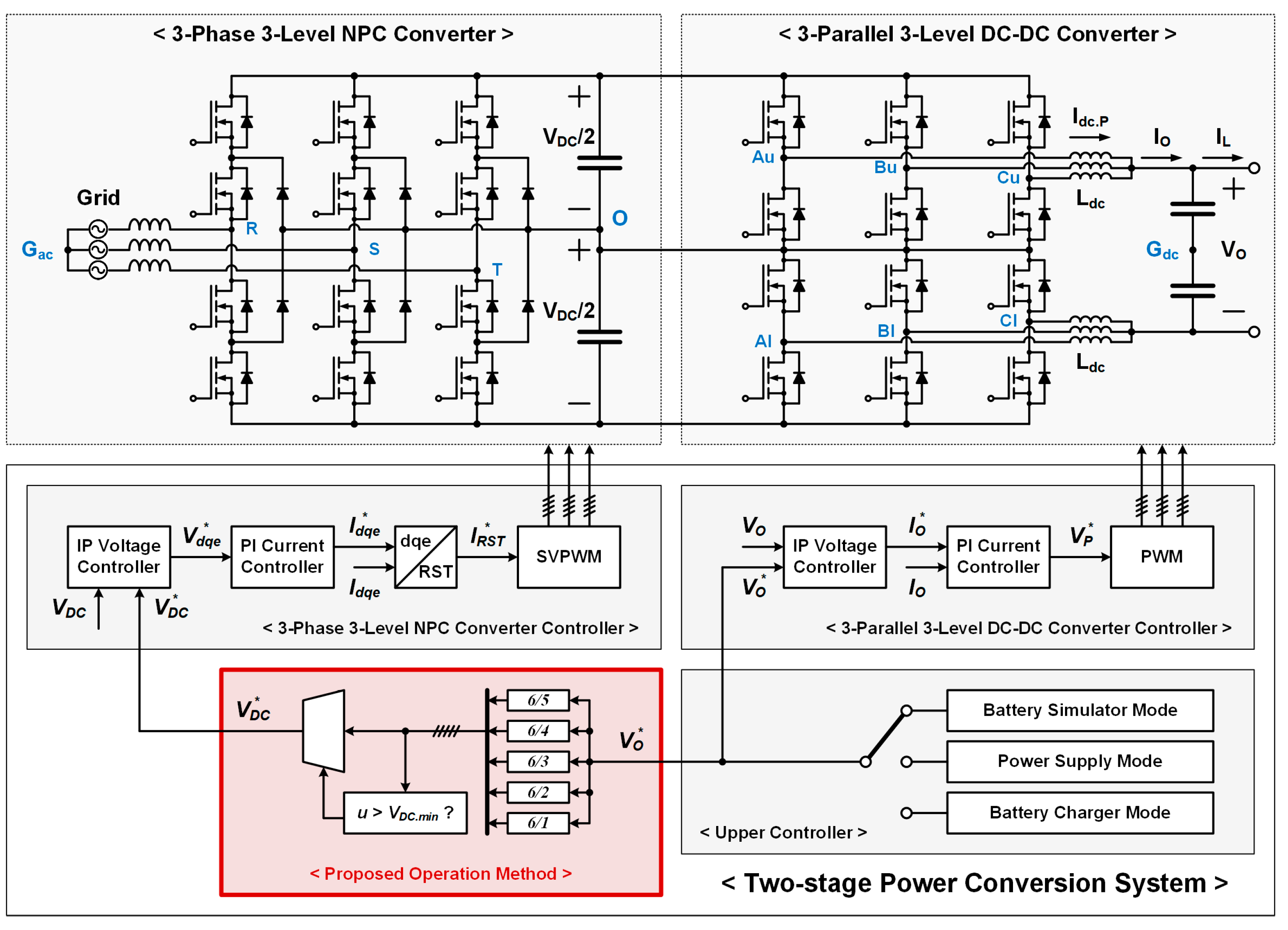
Figure 7 shows a control block diagram of the two-stage power conversion system, including the proposed operation method. The three-phase three-level NPC converter and three-parallel three-level DC–DC converter have a structure in which the voltage controller and current controller using the PID control are formed in series, respectively. Additionally, the upper controller outputs the output voltage command of the DC–DC converter according to each mode depending on the application of the two-stage power conversion system, such as the battery simulator, DC power supply, and battery charger. The output voltage command is input into the voltage controller of the DC–DC converter. Additionally, 6/5, 6/4, …, and 6 multiples of the output voltage command are compared with the minimum DC link voltage of the PWM converter and converted into the DC link voltage command according to priority, in order to reduce the DC inductor current ripple without increasing the output current ripple. Using the proposed operation method, the DC link voltage command is input into the voltage controller of the PWM converter.
4. Simulation Results
The effectiveness of the proposed two-stage power conversion system is demonstrated by various simulations through MATLAB Simulink. The system specifications of these simulations are shown in
Table 1, and they are the same as the system specifications used in the experiments. The switching frequency and current control frequency of the PWM converter and DC–DC converter are 50 kHz, and the voltage controller of each converter is controlled at 5 kHz.
In this paper, the DC output voltage command of the DC–DC converter is set as the ramp input, increasing from 275 V to 420 V, to output a voltage in the general range of the electric vehicle battery.
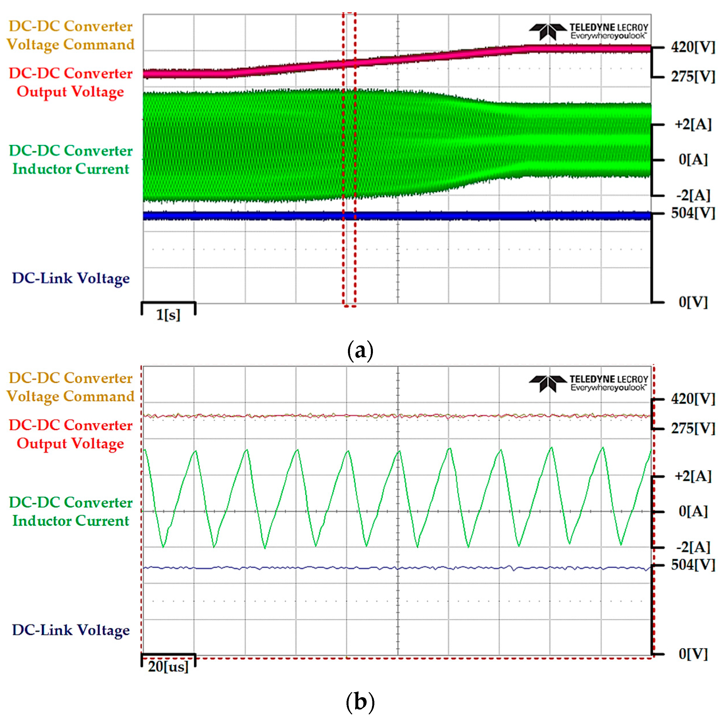
Figure 8a shows the simulation results for the voltage command, output voltage, DC inductor current, and DC link voltage of the two-stage power conversion system, when the DC link voltage is constantly controlled to 504 V through the PWM converter as the general operation method of the system. Since the DC link voltage is constant and the output voltage increases, the output voltage duty ratio of the DC–DC converter increases. Accordingly, the inductor current decreases according to the increasing output voltage. However, the DC inductor current is very large when the voltage and duty ratio are low.
Figure 8b shows an enlarged waveform from
Figure 8a when the DC–DC converter output voltage becomes 320 V. From Equation (14), the DC inductor current ripple calculated through the system parameters and input/output voltage of the DC–DC converter is about 5.71 A. The simulated DC inductor current ripple is also almost the same as the calculated ripple magnitude.
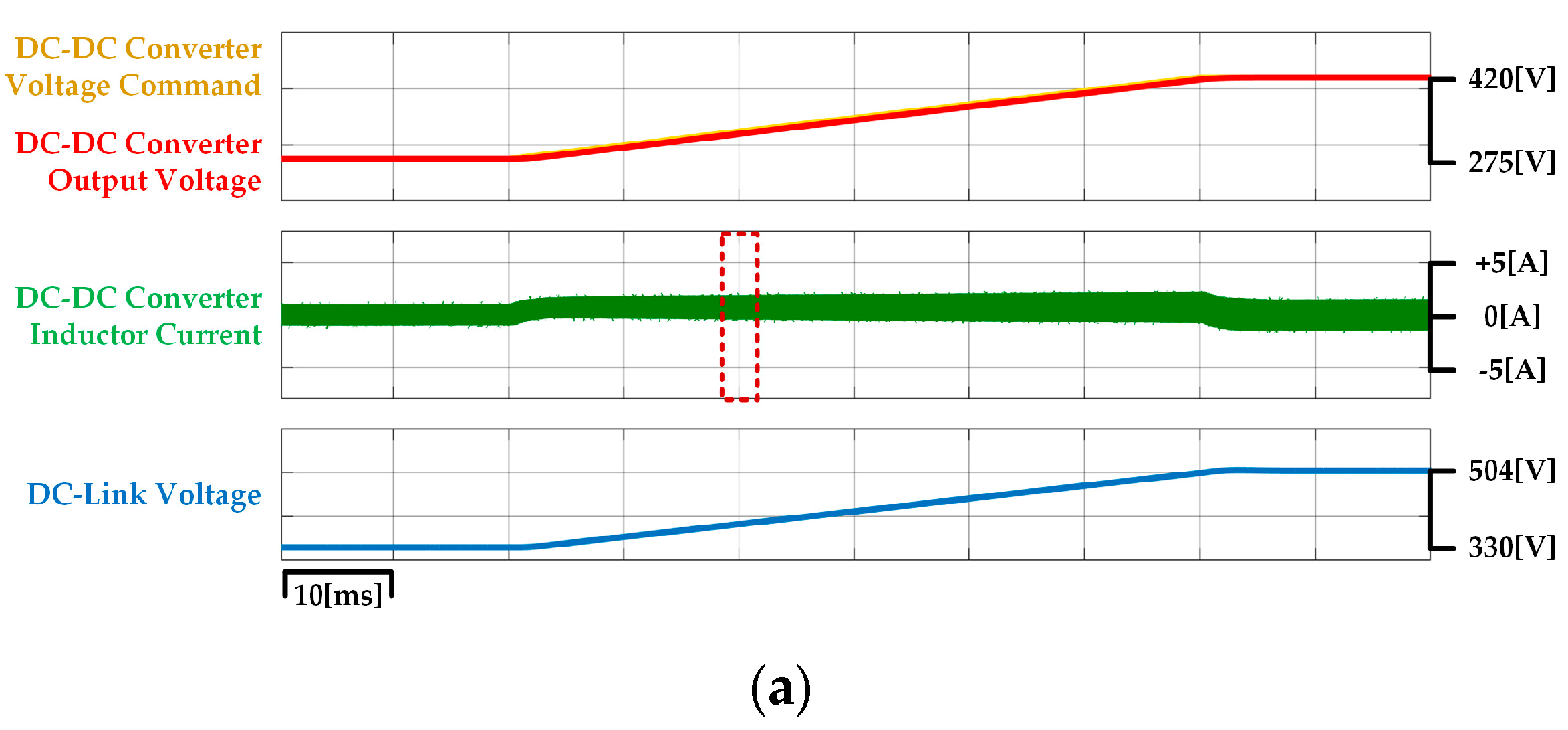
Figure 9a illustrates the simulation results when the DC link voltage is properly controlled according to the output voltage by using the proposed method. The DC link voltage is controlled from 330 V to 504 V as the output voltage increases from 275 V to 420 V. The DC inductor current ripple significantly decreases at a low output voltage compared to
Figure 8a. The duty ratio is maintained, but the DC inductor current ripple gradually increases because the output voltage increases. When the output voltage becomes 420 V, the DC link voltage becomes 504 V, as in
Figure 8a, and the DC inductor current ripple is also the same.
Figure 9b shows the enlarged waveform of the DC inductor current at the point where the DC–DC converter output voltage becomes 320 V in
Figure 9a. The calculated DC inductor current ripple is about 2.13 A, and the simulation result is also about the same.
Figure 10 and
Figure 11 show the simulation results when adding a 120 Ω load under the same simulated conditions of
Figure 8 and
Figure 9, respectively. Even though the DC inductor current is increased by the load, the DC inductor current ripple is almost identical to that in
Figure 8 and
Figure 9 under no load conditions.
5. Experimental Results
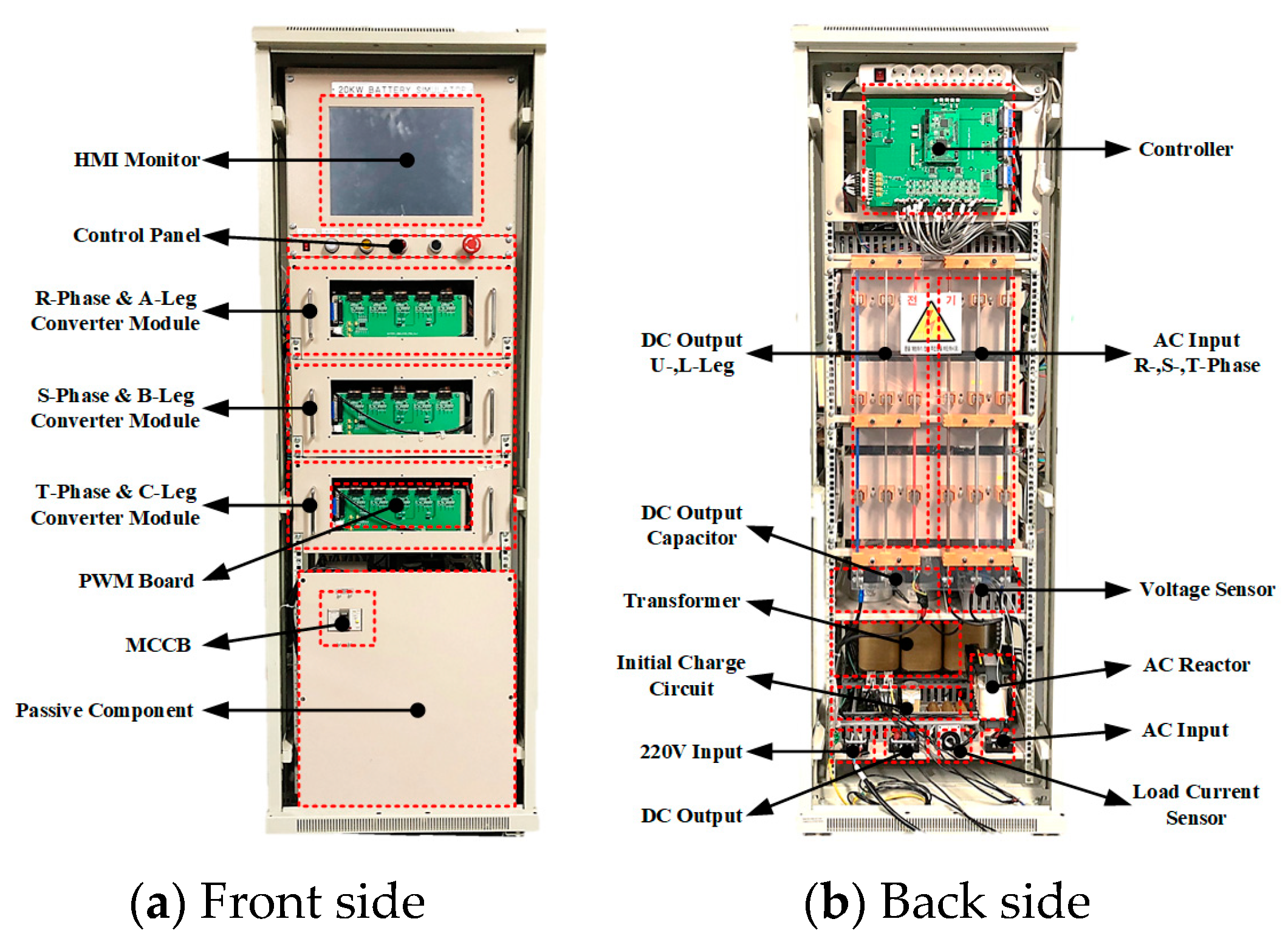
The validity of the proposed method was confirmed through the simulations. To further confirm the simulation results, we set up experiments with the two-stage power conversion system including the three-phase three-level NPC converter and the three-parallel three-level DC–DC converter, as shown in
Figure 12. This setup consisted of three power converter modules, AC inductors, DC–DC converter output capacitors, and a control board.
As shown in
Figure 13a, each module consisted of one leg of the DC–DC converter and PWM converter. DC inductors, current sensors, and DC link capacitors were also included in the module. The power semiconductor switch used for the PWM converter and DC–DC converter was CREE’s all-silicon carbide MOSFET Half-Bridge Module CAS120M12BM2. As shown in
Figure 13b, the system was controlled by the control board, including TI’s MCU TMS320F28377D and ALTERA’s FPGA EP4CE40F23I8LN.
Details of the system parameters are shown in
Table 1. The switching frequency and current control frequency of the PWM converter and DC–DC converter were 50 kHz, as in the simulations. The voltage controller of each converter was also controlled at 5 kHz.
Figure 14a shows the experimental results under a constant DC link voltage with no load. The operation sequence was the same as in
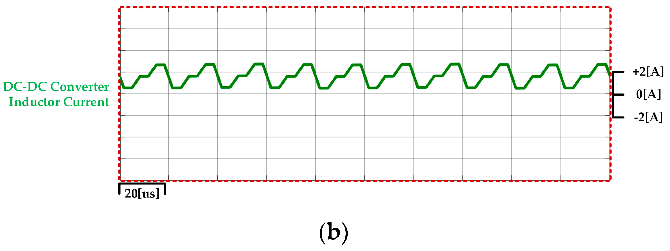
Figure 8a, but the experiments were performed at 1s/division, unlike the simulation, to minimize the effect of the transient state of the DC–DC converter voltage control. Through this operation, the average of the DC inductor current under no load conditions was zero.
Figure 14a represents the same experimental results, except with the average DC inductor current.
Figure 14b illustrates the DC inductor current with a DC link voltage of 320V; the difference from the calculated ripple magnitude is larger than the simulation results in
Figure 8b. This difference was caused by the voltage drop component of the system, the dead time of the switch, the tolerance of the DC inductor, and so on.
Figure 15a shows the experimental results when using the proposed method with no load. The operation sequence and the experimental results were the same as in
Figure 9a, except for the average DC inductor current.
Figure 15b illustrates the DC inductor current under a DC link voltage of 320V, and the difference from the calculated ripple magnitude is larger than the simulation results in
Figure 9b. However, since the magnitude of the current ripple was reduced by less than half compared to
Figure 14b when controlled by the constant DC link voltage, it can be confirmed that the proposed method was effective at reducing the current ripple. Additionally, the inductance of the DC inductor was inversely proportional to the magnitude of the current ripple, as shown in Equation (14). Therefore, the proposed method could reduce the inductance of the DC inductor as much as the current ripple decreased under the condition that the maximum magnitude of the current ripple was the same.
Figure 16 and
Figure 17 show the experimental results of adding a 120 Ω load under the experimental conditions of
Figure 14 and
Figure 15, respectively. Even though the average of the DC inductor current increased with the load, the DC inductor current ripple was almost identical to that in
Figure 14 and
Figure 15 under no load conditions. Therefore, the proposed method was also proven to be valid for DC inductor current ripple reduction under load conditions.


 ,
, 


