Abstract
This paper presents a 52-to-57 GHz CMOS quadrature voltage-controlled oscillator (QVCO) with a novel I/Q phase tuning technique based on a body bias control method. The QVCO employs an in-phase injection-coupling (IPIC) network comprising four diode-connected FETs for the quadrature phase generation. The I/Q phase error is calibrated by controlling the body bias voltage offset of the QVCO’s four core FETs. This technique effectively covers a wide range of I/Q phase error between −13.4° and +10.7°. It also minimally induces the unwanted variations in the phase noise, current dissipation, and oscillation frequency, which were found to be only 0.4 dB, 0.07%, and 36 MHz, respectively. After the IPIC-QVCO, a phase-tunable two-stage LO buffer employing a 3-bit switched-capacitor bank was added for additional phase tuning, leading to the extension of the phase tuning range up to −22.7–+20.0°. The proposed QVCO is implemented in a 40 nm RF CMOS process. The measured results show that the QVCO covers a frequency band from 52.4 to 57.6 GHz while consuming 26.2 mW. The phase noise and the figure-of-merit of the QVCO are −91.8 dBc/Hz at 1 MHz offset and −172.4 dBc/Hz, respectively. We also realized a fully integrated 55 GHz quadrature RF transmitter employing the phase-tunable QVCO and LO generator. The effectiveness of the proposed phase-tunable LO generator was confirmed by verifying the image rejection ratio (IRR) calibration at the RF output.
1. Introduction
With the fast-growing demand for 60 GHz band wireless applications such as radar sensors [,] and short-range connectivity [], this band has been attracting lots of research and development efforts. To produce single-chip RF transceivers for 60 GHz wireless applications, a quadrature transceiver architecture is widely adopted. This is because 60 GHz wireless communication usually employs quadrature modulation and demodulation schemes such as quadrature amplitude modulation (QAM) to achieve a high data rate [,,]. One of the challenges in designing a quadrature transceiver is the I/Q phase imbalance in the I/Q LO signals. The I/Q phase error is known to cause severe performance degradations in the signal-to-noise ratio (SNR) and image rejection ratio (IRR). Therefore, an efficient and precise calibration technique for the I/Q phase error is essentially needed for the quadrature LO generation in CMOS technology.
The quadrature LO generation in CMOS can be realized in various manners. A 2 × fo voltage-controlled oscillator (VCO) and a subsequent divide-by-two circuit are widely employed due to the simple design and high I/Q accuracy. Unfortunately, however, this approach would not be practical for the 60 GHz band, because the required 120 GHz VCO would be too challenging. An RC-CR polyphase filter connected after a fundamental fo VCO is another possible approach, as can be found for 28 GHz transceivers [,]. However, in the 60 GHz band, improving the I/Q mismatch and insertion loss of the RC-CR filter imposes too great a challenge. Meanwhile, in order to alleviate the VCO design requirements in the quadrature LO generator, an injection-locked frequency tripler (ILFT) has been reported [,,,]. In [,], a tunable phase shifter was employed to generate quadrature LO signals at fo/3, which were then tripled by a subsequent ILFT. This approach, however, would make it difficult to achieve accurate I/Q phase tuning, since the ILFT triples not only the frequency but also the phase error. Another approach is to employ a phase-tunable quadrature ILFT, as can be found in the 60 GHz [] and 28 GHz [] bands. These employ a phase-tunable bottom-series-coupled QVCO (BS-QVCO), which tunes the I/Q phase by controlling the QVCO’s varactors at the fundamental frequency fo in a fine step. However, this approach suffers from a narrow locking range due to the inherent injection-locking characteristics.
In contrast to the above methods, direct use of a fundamental QVCO with phase-tuning capability should show the best advantages of simple circuitry and a wide tuning range. However, the phase error can be as high as several degrees unless it is accompanied by proper phase-tuning circuitry [,,,,,,,]. The parallel-coupled fundamental QVCOs (P-QVCOs) in 60 GHz [] and 50 GHz [] did not report any phase-tuning technique; thus, a phase error as poor as 2.5 degrees was found in []. Magnetic-coupled QVCOs [,,] also reported about 1.5 degrees of phase error at 60 GHz without any phase-tuning circuitry. On the other hand, a superharmonic-coupled 60 GHz QVCO (SH-QVCO) in [] employed an independent varactor tuning at the two VCO cores to compensate for the I/Q phase error. However, the phase error was as poor as ±5 degrees. In [], a 45 GHz SH-QVCO employed a tunable transconductance (gm) stage in the coupling network to compensate for the I/Q phase error within 0.3 degrees, but its phase-tuning range was too limited at only +0.1–+2.5 degrees.
Meanwhile, it has been found that an in-phase injection-coupled (IPIC) QVCO with a diode-based coupling network [,] is an effective and efficient fundamental QVCO architecture due to its class-C-like operation and low phase-noise performances. Indeed, the 60 GHz IPIC-QVCO in [] showed excellent phase matching, but no phase-tuning circuitry was reported. Hence, in this work, we present a 60 GHz IPIC-QVCO with a novel I/Q phase-tuning capability based on a body bias control of the VCO core FETs. A theoretical analysis is described to prove how the body bias control can induce the phase tuning in the IPIC-QVCO. Implemented in a 40 nm CMOS process, the 60 GHz IPIC-QVCO showed a wide I/Q phase tuning range of −13.4–+10.7 degrees. Furthermore, with an additional phase-tunable LO buffer attached after the IPIC-QVCO, the phase-tuning range was extended to −22.7–+20.0 degrees. In order to prove the I/Q phase-tuning performance, the complete QVCO and LO generator was fully integrated in a 60 GHz quadrature RF transmitter [], demonstrating that the IRR at the RF transmitter output is dramatically improved by the proposed phase-tuning technique.
2. Circuit Design
2.1. Phase-Tunable In-Phase Injection-Coupled (IPIC) QVCO
Figure 1 shows the circuit schematic of the phase-tunable IPIC-QVCO. It comprises two cross-coupled negative-gm VCO cores and a coupling network in between to create the desired quadrature phase. The coupling network comprises four diode-connected n-FETs (Mc1–4). It injects coupling currents into the VCO cores at the aligned phase, realizing the in-phase injection coupling of the two VCO cores and leading to the desired quadrature VCO operation. The frequency tuning characteristics are achieved through the 3-bit discrete-tuned switched-capacitor bank Ct<2:0> for producing eight sub-band tuning curves and the MOS varactor diodes Cv for producing a continuously tuned curve within each sub-band tuning curve. The switched-capacitor bank circuit has a conventional design, as can be found in many previous papers [,,].
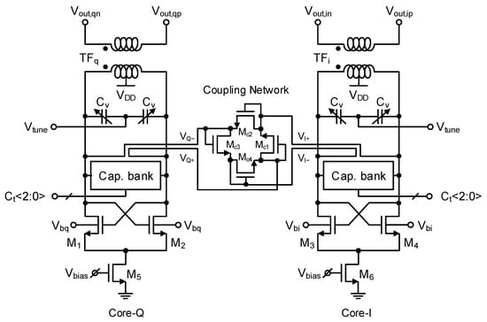
Figure 1.
Proposed QVCO schematic.
The I/Q phase error should be caused by the mismatches of the VCO cores and the coupling network. Without any calibration, the I/Q phase error typically reaches a few degrees in millimeter-wave CMOS QVCOs [,,,,,,,]. Hence, this work proposes a novel I/Q phase-tuning technique in order to suppress the phase error to a negligible sub-degree level. The proposed tuning method intentionally offsets the individual oscillation frequencies of the two VCO cores by tuning the body bias voltages Vbi and Vbq of the n-FETs M3,4 and M1,2, respectively. From the initial value of 0.25 V, the Vbi and Vbq are changed by the same amount but in opposite directions, enabling the desired I/Q phase calibration without a significant change in the oscillation frequency.
Before we further describe the details of the I/Q phase-calibration technique, let us first examine the operating principle of the IPIC-QVCO. Figure 2a illustrates one of the diode-connected n-FETs, Mc2, of the coupling network shown in Figure 1. As shown in Figure 1, the gate terminal of Mc2 is connected to the VI+ node of VCO core I, while the source terminal is connected to the VQ− node of the other VCO core Q. As shown in Figure 2b, VI+ has the same amplitude and frequency as VQ−, but its phase is shifted by 90 degrees. Therefore, Vgs of Mc2 (=VI+ − VQ−) is formed at 45 degrees behind VI+. Since Mc2 turns on only when Vgs exceeds the threshold voltage, Mc2’s drain current Ic2 should be created in phase with Vgs. Similar to Ic2, Mc1’s drain current Ic1 is 45 degrees behind VQ+. Thus, Ic1 should be in phase with Mc1’s Vgs, and Ic1 is 90 degrees behind Ic2.
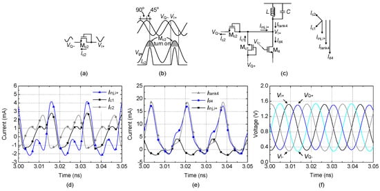
Figure 2.
Operating principle of the in-phase injection coupling in the QVCO: (a) diode-connected coupling FET and (b) its turn-on operation. (c) Current flow diagram at the VCO core and the coupling network. Simulated current and voltage waveforms: (d) Ic1, Ic2, and Iinj,i+; (e) Iinj,i+, Itank4, and Id4; and (f) final quadrature output voltages VI+, VQ+, VI−, and VQ−.
Figure 2c visualizes the current flow vector of the coupling network. The injection current Iinj,i+ flowing from the coupling network into the core VCO is given by Ic1 − Ic2. Since Ic1 has the same amplitude with Ic2 and is 90 degrees behind that of Ic2, the phase of Iinj,i+ should be 45 degrees behind Ic1. Consequently, Iinj,i+ is in phase with the node voltage VI+ and the drain current Id4 of the core FET M4, as well as with the tank current Itank4. Through the same analysis, we can know that the four signals VI+, VQ+, VI−, and VQ− are set to differential I/Q signals.
The above operating principle of the IPIC-QVCO was verified by circuit simulations. Figure 2d–f show the simulated time-domain voltage and current waveforms at the IPIC-QVCO. Figure 2d shows Ic1, Ic2, and Iinj,i+. It is confirmed that Ic1 and Ic2 have a phase difference of 90 degrees, while Iinj,i+ is 45.9 degrees behind Ic1. In Figure 2e, it can be observed that Itank4 and Id4 are aligned well, while Iinj,i+ shows slight misalignment with Itank4 and Id4. In spite of the slight misalignment, the quadrature phase relationships between Ic1 and Ic2 (as shown in Figure 2d) and between VI+,− and VQ+,− (as shown in Figure 2f) prove that the in-phase injection locking of the QVCO works properly to generate the quadrature output signals at the QVCO. The whole operation can be confirmed by observing the four output voltages VI+, VQ+, VI−, and VQ− in Figure 2f (with an amplitude of 0.62 V and a frequency of 58 GHz). We can confirm that the IPIC-QVCO produces the desired differential quadrature phase output signals properly.
When we apply a body bias voltage at the QVCO, the body leakage of the FETs must be carefully monitored. Figure 3 shows the simulated leakage current flowing through the body terminal of the core’s FET when the QVCO oscillates with the body bias voltage swept from 0 to VDD. Both the peak and average values of the body leakage current are plotted for the sake of comparison. As can be seen, when the body bias voltage exceeds 0.5 V, the body current begins to rapidly increase. This will result in an unacceptable increase in the dynamic current consumption of the QVCO, which, in turn, will lead to undesirable performance degradations in the phase noise and I/Q phase error of the QVCO. Thus, we set the maximum limit of the body bias voltage to 0.5 V. Through simulations, we found that the QVCO’s current consumption is increased by 20 μA when the body bias voltage is set to 0.5 V, which is only a 0.07% change compared to the nominal consumption of 29.1 mA.
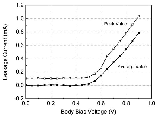
Figure 3.
Simulated body leakage current.
Yi et al. [] derived an analytic relation of the I/Q phase error in the QVCO with respect to the oscillation frequency offset of the two VCO cores. is given by
where is a damping coefficient and is the nominal oscillation frequency of the QVCO. The damping coefficient is given by
where is the LC tank quality factor, is the coupling strength, is the tail current of the QVCO, and and are the transconductance and threshold voltage of the coupling diode-connected FET, respectively. The coupling strength is expressed as
where is the injection current and is the VCO’s tank current. Since the tank current is supplied by the tail current source through the hard-limiting switching operation of the core FETs, and the tank is sufficiently high, only the fundamental component of the tank current can be taken into account, which is .
Based on the Equations (1)–(3), we can calculate the theoretical phase-tuning range of the QVCO. By conducting DC and transient simulations of the designed VCO circuit shown in Figure 1, we first estimated the required parameter values of (58.5 GHz), tank (7.6), (13.8 mA), and (3.0 mA). Since is , is 8.78 mA. Then, the coupling strength was computed to 0.342. In addition, the and of the coupling diodes Mc1–4 were found through transient simulations to be 9.32 mS and 454.5 mV at 58.5 GHz, respectively. Finally, the damping coefficient was computed to 23.04 using Equation (1). As a next step, we found through transient simulations that the VCO core’s oscillation frequency increases by 400 MHz when the body bias voltage increases by 0.5 V. Finally, we computed the theoretical phase-tuning range to be 9.03 degrees using Equation (1). It should be noted that and in Equation (1) remain almost unchanged against the body bias voltage control. Therefore, we can conclude that the body bias control only changes (and, therefore, the phase error ) according to Equation (1).
The theoretical prediction given by Equations (1)–(3) was verified through circuit simulations. Figure 4a shows the simulated frequency offset and phase error against the body bias voltage offset ∆Vb = Vbi − Vbq. In this design, the initial values of Vbi and Vbq were set at +0.25 V, so that the initial ∆Vb and were all set to zero. Then, the Vbi and Vbq were tuned by the same amount but in opposite directions, while the maximum Vbi and Vbq were limited to 0.5 V. As a result, ∆Vb was tuned between −0.5 and +0.5 V. As shown in Figure 4a, the frequency offset and the phase error were found to change from −390 to +390 MHz and from −7.1 to +8.7 degrees, respectively, across the entire range of ∆Vb. Figure 4b compares the simulated and theoretically calculated phase error versus the frequency offset . The theoretical data were calculated from Equation (1), and the simulated data were obtained from Figure 4a. We found that the calculated data agreed very well with the simulated results, confirming that the proposed I/Q phase-tuning calibration technique is valid and effective. Meanwhile, we investigated how the phase noise is affected by the body bias control. Figure 4c shows the simulated phase noise against ∆Vb. It demonstrates that the phase noise changes only by 0.3 dB across the ∆Vb tuning range. Thus, it confirms that our proposed phase-tuning technique minimally impacts the phase noise performance of the QVCO.
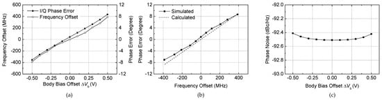
Figure 4.
(a) Simulated frequency offset and I/Q phase error against the body bias voltage offset ∆Vb = Vbi − Vbq (Vbi = Vbq = 0.25 V when ∆Vb = 0 V). (b) Simulated and theoretically computed I/Q phase error against the frequency offset. (c) Simulated phase noise against ∆Vb.
The robustness of the proposed phase-tuning technique against the PVT corner variations was examined. Figure 5 shows the simulated I/Q phase error, oscillation frequency, and phase noise versus the body bias offset ∆Vb under seven PVT corners. The seven corners include two process corner conditions of SS and FF, two voltage corner conditions of 0.81 V and 0.99 V, and two temperature corner conditions of −40 °C and +80 °C, from the nominal condition having the typical process corner of TT, typical VDD of 0.9 V, and typical temperature of +27 °C.
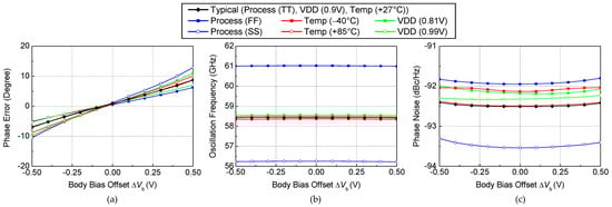
Figure 5.
Results of seven PVT corner simulations: (a) I/Q phase error, (b) oscillation frequency, and (c) phase noise, all against the body bias offset ΔVb.
Figure 5a shows that the phase-tuning range varies with respect to seven corners, with typical, maximum, and minimum ranges of −7.1–+8.7, −10.6–+12.9, and −5.1–+6.3 degrees, respectively. We found that even the minimum tuning range is acceptable for our 60 GHz LO generator design application when we add an additional phase-tunable LO buffer, as described in Section 2.2. Figure 5b shows that the oscillation frequency would change by as much as 2.5 GHz across the FF and SS corners; however, it does not change significantly against ∆Vb (which is only 36 MHz). This indicates that the proposed body bias control technique does not induce significant oscillation frequency and performance variations. Figure 5c also shows that the body bias control does not cause significant changes in the phase noise performance (only 0.2–0.3 dB), although it may change more against the corners.
2.2. Quadrature LO Generator with the Proposed QVCO and Phase-Tunable Buffer
A complete quadrature LO generator including the proposed QVCO was designed by adding a phase-tunable LO buffer after the QVCO. The architecture of the quadrature LO generator is shown in Figure 6. The VCO buffer isolates the QVCO’s LC tank from the subsequent loading effect. The two-stage phase-tunable LO buffer gives additional phase tunability, thereby extending the overall I/Q phase-tuning performance significantly.
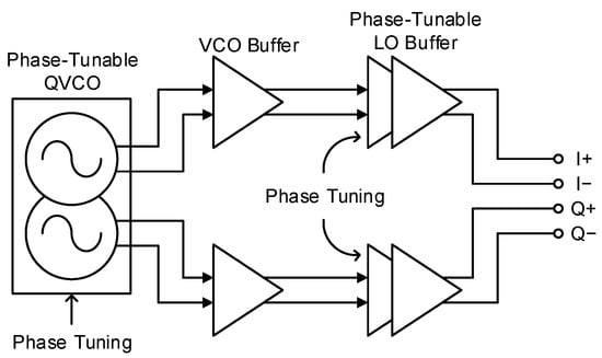
Figure 6.
Block diagram of the entire quadrature LO generator.
Figure 7 shows the schematic of the VCO buffer and the phase-tunable LO buffer. They were designed in a fully differential stage with a tail current source in order to improve the common-mode noise immunity. Note that the transformer TR1 shown in Figure 7 indicates the coupling transformer TRi,q at the VCO output in Figure 1. The small signal gain of the buffer stage was designed as high as 21.9 dB to guarantee sufficient swing at the output. Note that the phase-tuning capability of the LO buffer was realized by using 3-bit discrete tuned capacitor banks in the two stages. The same approach for the phase-tunable LO buffer design can be found in [,].
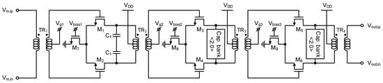
Figure 7.
Schematic of the single-stage VCO buffer and the phase-tunable two-stage LO buffer.
The current dissipation is 5.6 mA for the first-stage VCO buffer, and 10.1 mA for the second- and third-stage LO buffer.
Figure 8 shows the simulated performance of the overall phase-tuning characteristics of the entire quadrature LO generator. The I/Q phase tuning is first achieved by controlling the body bias offset ∆Vb between −0.5 and +0.5 V, as noted by the (0,0)-curve in Figure 8. This shows the phase-tuning range of −13.4 to +10.7 degrees. It is interesting to note that it becomes slightly wider than the original tuning range of the QVCO alone without the buffer, as shown in Figure 4b. Now, in addition to the ∆Vb tuning, the phase-tunable LO buffer is simultaneously tuned using the 3-bit switched-capacitor banks. Since we have two stages for the phase-tunable buffer, the tuning code can be set to 64 different codes between (0,0) and (7,7). In Figure 8, only nine selected states (the lowest code 0, the middle code 4, and the highest code 7 for the first and second stages) are plotted. This clearly shows that the phase-tuning curve is shifted up and down with respect to the capacitor bank code, while the total tuning range against ∆Vb does not change much. The total tuning range from codes 0 to 7 for each LO buffer was found to be about 4–5 degrees, resulting in the overall tuning range of the QVCO including the LO buffer of 42.7 degrees (from −22.7 to +20.0 degrees). Thus, we can see that the proposed LO generator block gives a sufficiently wide tuning range. Note that the tuning accuracy is determined by the ∆Vb tuning resolution. We can estimate that the tuning accuracy will be 0.37° by assuming a 6-bit voltage digital-to-analog converter (VDAC) is used for ∆Vb tuning, as reported in our other works [,]. In this work, however, the VDAC circuit was not included in the QVCO, whereas the body bias voltage was directly tuned by using external voltage sources.
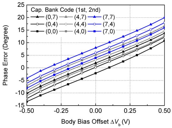
Figure 8.
Simulated overall phase-tuning characteristics of the quadrature LO generator.
3. Implementation Results
The IPIC-QVCO integrated circuit was fabricated in a 40 nm RF CMOS process. A die micrograph of the QVCO is shown in Figure 9a. Note that additional circuitry of a two-stage VCO buffer and a divide-by-eight frequency divider was included for test purposes. The total die area, including the pads, is 540 × 1150 μm2, while the QVCO core occupies 260 × 137 μm2, and the first- and second-stage VCO buffers occupy 240 × 132 and 110 × 120 μm2, respectively. The divide-by-eight frequency divider consists of three cascaded divide-by-two circuits, with individual areas of 268 × 130, 390 × 190, and 460 × 170 μm2, respectively. The QVCO consumes a current of 29.1 mA from a supply voltage of 0.9 V. The VCO buffers consume 28.7 mA, and the three divide-by-two circuits consume 11.9 mA, 7.2 mA, and 5.8 mA, respectively. The measurement setup for the QVCO is shown in Figure 9b. The QVCO output spectrum was measured by using a Keysight N9030B spectrum analyzer.
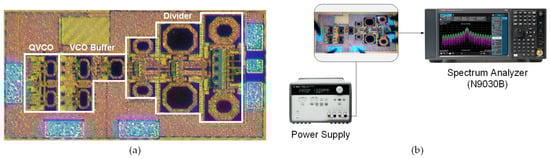
Figure 9.
(a) Die micrograph of the QVCO followed by a two-stage VCO buffer and a divide-by-eight frequency divider added for test purposes. (b) Measurement setup.
Figure 10 shows the output spectrum of the QVCO measured using a Keysight N9030B spectrum analyzer. Note that the measured frequency of 6.8 GHz should be multiplied by 8 to obtain the QVCO oscillation frequency of 54.4 GHz.
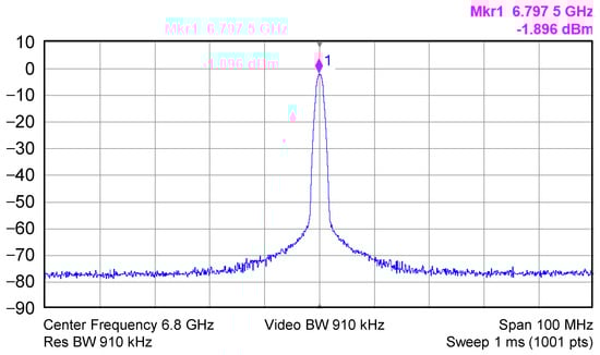
Figure 10.
Measured output spectrum of the QVCO after the divide-by-eight.
Figure 11a shows the measured QVCO frequency tuning range. With the 3-bit sub-band tuning, the eight discrete tuning curves are clearly exhibited. The tuning range of the QVCO is from 52.4 to 57.6 GHz, giving a total tuning range of 9.2 GHz. A slight frequency downshift from the simulation results is observed, which should be attributed to unexpected parasitic LC components in the fabricated circuit.
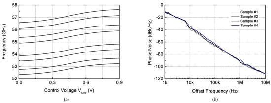
Figure 11.
Measured results: (a) frequency tuning range; (b) phase noise of four samples.
Figure 11b shows the phase noise performances of the QVCO measured from four samples. The measured phase noises were observed between −90.2 and −91.8 dBc/Hz at a 1 MHz offset for a 54.6 GHz oscillation frequency. This corresponds to the VCO’s figure-of-merit (FoM) of −170.8–−172.4 dBc/Hz. At 100 kHz and 10 MHz offsets, the phase noises from the four samples were also found to be −63.2–−66.9 dBc/Hz and −109.3–−112.0 dBc/Hz, respectively. The corner frequency dividing the 1/f3 and 1/f2 region was found to be less than 2 MHz, indicating a low flicker noise upconversion process.
For more complete verification of the phase-tuning operation of the proposed circuit, the quadrature LO generator comprising the IPIC-QVCO, VCO buffer, and phase-tunable LO buffer was fully integrated into the author’s 55 GHz quadrature RF transmitter []. Figure 12a,b show a die micrograph and the measurement setup of the fabricated RF transmitter, respectively. The total die area is 600 × 1380 μm2.
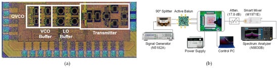
Figure 12.
(a) Die micrograph of the fully integrated quadrature RF transmitter employing the proposed QVCO and phase-tunable LO buffer. (b) Measurement setup.
The fabricated transmitter chip was mounted on a printed circuit board. DC and low-frequency signals were fed through wire-bonded pads, and RF signals were fed and probed by V-band on-wafer probes. For the output spectrum measurement, the QVCO was first set to oscillate at 56 GHz, and the baseband I/Q signals at 300 MHz were applied to the baseband input ports. Then, we could recognize that the transmitter’s output creates three tones: the LO leakage at 56 GHz, the desired tone at 56.3 GHz, and the unwanted image tone at 55.7 GHz.
Figure 13 demonstrates that the IRR at the RF transmitter output is improved by the phase-tuning capability of the QVCO and LO generator. Figure 13a shows the output spectrum before the phase calibration. The desired and image tones appear exactly 300 MHz away from the LO leakage tone, and the IRR is only −13.2 dB, which is unacceptably high. Figure 13b shows the worst case when the I/Q phase calibration is set to the worst condition, in which the IRR becomes as poor as −9.4 dB. Finally, Figure 13c shows the best condition obtained by setting the optimal I/Q phase calibration. The overall calibration procedure was as follows: we first performed the coarse tuning through the LO buffer capacitor bank calibration and, subsequently, further performed the fine tuning through the QVCO body bias calibration. We observed that the IRR was improved by up to −20.4 dB. It was also noted that the magnitude and frequency of the desired signal remained almost unchanged after the calibration, which implies that the proposed phase-calibration technique effectively provides a wide-ranging and highly accurate phase calibration without introducing significant changes in the LO amplitude and frequency. Thus, the proposed phase-calibration technique can ensure high-quality signal transmission at the 60 GHz millimeter-wave band.
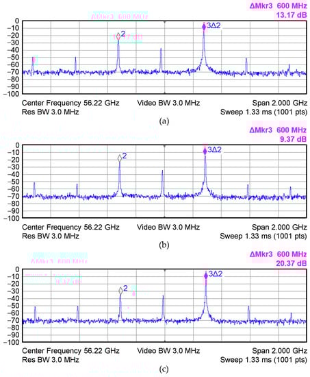
Figure 13.
Measured 56 GHz output spectrum at the RF transmitter output with the phase calibration set to (a) the default condition, (b) the worst condition, and (c) the best condition.
Table 1 summarizes the performances found in this work and compares them with other previous works. The previous mmWave QVCOs such as the P-QVCO [], magnetic-coupled QVCOs [,,], and IPIC-QVCO [] did not report any I/Q phase-calibration technique in their QVCOs. Thus, no tuning performances were found in their publications. Meanwhile, two SH-QVCOs reported that a certain form of I/Q phase-calibration technique was realized in their QVCOs [,]. The 60 GHz SH-QVCO in [] added additional varactors in each VCO core’s LC tank and tuned the varactor capacitances to calibrate the I/Q phase. However, they reported a slightly poor phase-calibration accuracy of ±5 degrees. The 45 GHz SH-QVCO in [] employed a tunable gm-stage-based coupling network for the phase calibration. However, it reported a very limited tuning range of less than 2.5 degrees.

Table 1.
Performance summary and comparison with the recent mmWave QVCOs.
In contrast, this work was based on a novel combined approach of the body bias voltage control for the QVCO and the switched-capacitor tuning for the LO buffer. It demonstrated a very wide tuning range of −22.7–+20.0 degrees with sub-degree accuracy. In order to measure the phase tunability in this work, we have shown that the entire I/Q LO generator comprising the QVCO and LO buffer is integrated with a 60 GHz quadrature RF transmitter, and the image rejection ratio at the RF transmitter output was examined to verify the phase-tuning performances. It is interesting to note that [] incorporated a downconversion mixer and verified the phase-tunability at the downconverted baseband signal, while [] incorporated an I/Q self-mixer to generate a DC voltage proportional to the I/Q phase error. Although the verification methods are all different, they are acceptable to verify the phase-tunability in the millimeter-wave circuit design. Meanwhile, the power consumption and phase noise of this work were found to be slightly worse than in [,], although it should be noted that this is not attributed to the proposed calibration technique.
4. Conclusions
A 55 GHz CMOS IPIC-QVCO with a noble I/Q phase-calibration technique was designed and implemented in a 40 nm RF CMOS process. For a wide and precise I/Q phase-tuning performance, the IPIC-QVCO employs body bias tuning for the QVCO core FETs. Theoretical and simulated analyses confirmed the operating principle and tuning performances of the proposed method. The overall tuning range was extended by additional phase-tunable LO buffers. The combined phase calibration covers a wide tuning range of 42.7 degrees, with sufficiently good accuracy of less than 1 degree. The prototype QVCO integrated circuit was fabricated in 40 nm RF CMOS process and verified through chip measurements. The fully integrated 55 GHz quadrature RF transmitter IC with the proposed LO generator successfully demonstrated significant improvements of IRR performances at the RF output. This proves that the proposed IPIC-QVCO and phase-tunable LO buffer should be instrumental for millimeter-wave CMOS quadrature LO generator circuit design.
Author Contributions
Conceptualization, Y.L. and H.S.; methodology, Y.L. and H.S.; validation, S.L., Y.L. and H.S.; formal analysis, S.L. and H.S.; investigation, S.L. and H.S.; data curation, S.L. and Y.L.; writing—original draft preparation, S.L., Y.L. and H.S.; writing—review and editing, S.L. and H.S.; visualization, S.L. and Y.L.; supervision H.S.; project administration, H.S.; funding acquisition, H.S. All authors participated in all other aspects. All authors have read and agreed to the published version of the manuscript.
Funding
This research was supported by the National Research Foundation (NRF) of Korea under Grant 2020R1A2C1008484.
Data Availability Statement
Data sharing not applicable.
Acknowledgments
This work was conducted during a sabbatical year from Kwangwoon University in 2021. The computer-aided circuit design tools of this work were supported by the IC Design and Education Center of Korea (IDEC).
Conflicts of Interest
The authors declare no conflict of interest. The funders had no role in the design of the study; in the collection, analyses, or interpretation of data; in the writing of the manuscript; or in the decision to publish the results.
References
- Lien, J.; Gillian, N.; Karagozler, M.E.; Amihood, P.; Schwesig, C.; Olson, E.; Raja, H.; Poupyrev, I. Soli: Ubiquitous Gesture Sensing with Millimeter Wave Radar. ACM Trans. Graph. 2016, 35, 142. [Google Scholar] [CrossRef]
- Shopov, S.; Girma, M.G.; Hasch, J.; Cahoon, N.; Voinigescu, S.P. Ultralow-Power Radar Sensors for Ambient Sensing in the V-Band. IEEE Trans. Microw. Theory Tech. 2017, 65, 5401–5410. [Google Scholar] [CrossRef]
- Zhou, P.; Cheng, K.; Han, X.; Fang, X.; Fang, Y.; He, R.; Long, Y.; Liu, Y. IEEE 802.11 ay-based mmWave WLANs: Design Challenges and Solutions. IEEE Commun. Surv. Tutor. 2018, 20, 1654–1681. [Google Scholar] [CrossRef]
- Wu, R.; Minami, R.; Tsukui, Y.; Kawai, S.; Seo, Y.; Sato, S.; Kimura, K.; Kondo, S.; Ueno, T.; Fajri, N.; et al. 64-QAM 60-GHz CMOS Transceivers for IEEE 802.11ad/ay. IEEE J. Solid-State Circuits 2017, 52, 2871–2891. [Google Scholar] [CrossRef]
- Ha, J.K.; Noh, C.K.; Lee, J.S.; Kang, H.J.; Kim, Y.M.; Kim, T.H.; Jung, H.N.; Lee, S.H.; Cho, C.S.; Kim, Y.J. RF Transceiver for the Multi-Mode Radar Applications. Sensors 2021, 21, 1563. [Google Scholar] [CrossRef] [PubMed]
- Lee, Y.; Kim, S.; Shin, H. A 55-GHz Highly Linear Direct RF Transmitter in 40 nm CMOS. In Proceedings of the 17th European Microwave Integrated Circuits Conference (EuMIC), Milan, Italy, 26–27 September 2022; pp. 177–180. [Google Scholar]
- Piri, F.; Bassi, M.; Lacaita, N.; Mazzanti, A.; Svelto, F. A > 40 dB IRR, 44% Fractional-Bandwidth Ultra-Wideband mm-Wave Quadrature LO Generator for 5G Networks in 55 nm CMOS. In Proceedings of the International Solid-State Circuits Conference (ISSCC), San Francisco, CA, USA, 11–15 February 2018; pp. 368–370. [Google Scholar]
- Lee, Y.; Kim, S.; Shin, H. A 24 GHz CMOS Direct-Conversion RF Receiver with I/Q Mismatch Calibration for Radar Sensor Applications. Sensors 2022, 22, 8246. [Google Scholar] [CrossRef] [PubMed]
- Wu, L.; Leung, H.F.; Li, A.; Luong, H.C. A 4-Element 60-GHz CMOS Phased-Array Receiver with Beamforming Calibration. IEEE Trans. Circuits Syst. I Reg. Pap. 2017, 64, 642–652. [Google Scholar] [CrossRef]
- Wu, L.; Li, A.; Luong, H.C. A 4-Path 42.8-to-49.5 GHz LO Generation with Automatic Phase Tuning for 60 GHz Phased-Array Receivers. IEEE J. Solid-State Circuits 2013, 48, 2309–2322. [Google Scholar] [CrossRef]
- Siriburanon, T.; Kondo, S.; Katsuragi, M.; Liu, H.; Kimura, K.; Deng, W.; Okada, K.; Matsuzawa, A. A Low-Power Low-Noise mm-Wave Subsampling PLL Using Dual-Step-Mixing ILFD and Tail-Coupling Quadrature Injection-Locked Oscillator for IEEE 802.11ad. IEEE J. Solid-State Circuits 2016, 51, 1246–1260. [Google Scholar] [CrossRef]
- Kim, H.-T.; Park, B.-S.; Song, S.-S.; Moon, T.-S.; Kim, S.-H.; Kim, J.-M.; Chang, J.-Y.; Ho, Y.-C. A 28-GHz CMOS Direct Conversion Transceiver with Packaged 2 × 4 Antenna Array for 5G Cellular System. IEEE J. Solid State Circuits 2018, 53, 1245–1259. [Google Scholar] [CrossRef]
- Scheir, K.; Vandersteen, G.; Rolain, Y.; Wambacq, P. A 57-to-66 GHz Quadrature PLL in 45 nm Digital CMOS. In Proceedings of the International Solid-State Circuits Conference (ISSCC), San Francisco, CA, USA, 8–12 February 2009; pp. 494–496. [Google Scholar]
- Chang, H.-Y.; Chan, C.-C.; Li, S.-M.; Yeh, H.-N.; Shen, I.Y.-E.; Huang, G.-L. Design and Analysis of CMOS Low-Phase-Noise Low Quadrature Error V-Band Subharmonically Injection-Locked Quadrature FLL. IEEE Trans. Microw. Theory Tech. 2018, 66, 2851–2866. [Google Scholar] [CrossRef]
- Decanis, U.; Ghilioni, A.; Monaco, E.; Mazzanti, A.; Svelto, F. A Low-Noise Quadrature VCO Based on Magnetically Coupled Resonators and a Wideband Frequency Divider at Millimeter Waves. IEEE J. Solid-State Circuits 2011, 46, 2943–2955. [Google Scholar] [CrossRef]
- Wu, L.; Luong, H.C. A 49-to-62 GHz Quadrature VCO with Bimodal Enhanced-Magnetic-Tuning Technique. IEEE Trans. Circuits Syst. I Reg. Pap. 2014, 61, 3025–3033. [Google Scholar] [CrossRef]
- Xi, T.; Guo, S.; Gui, P.; Huang, D.; Fan, Y.; Morgan, M. Low-Phase-Noise 54-GHz Transformer-Coupled Quadrature VCO and 76-/90-GHz VCOs in 65-nm CMOS. IEEE Trans. Microw. Theory Tech. 2016, 64, 2091–2103. [Google Scholar] [CrossRef]
- Szortyka, V.; Shi, Q.; Raczkowski, K.; Parvais, B.; Kuijk, M.; Wambacq, P. A 42 mW 200 fs-Jitter 60 GHz Sub-Sampling PLL in 40 nm CMOS. IEEE J. Solid-State Circuits 2015, 50, 2025–2036. [Google Scholar] [CrossRef]
- Zhang, L.; Kuo, N.-C.; Niknejad, A.M. A 37.5–45 GHz Superharmonic-Coupled QVCO with Tunable Phase Accuracy in 28 nm CMOS. IEEE J. Solid-State Circuits 2019, 54, 2754–2764. [Google Scholar] [CrossRef]
- Yi, X.; Boon, C.C.; Liu, H.; Lin, J.F.; Lim, W.M. A 57.9-to-68.3 GHz 24.6 mW Frequency Synthesizer with In-Phase Injection-Coupled QVCO in 65 nm CMOS Technology. IEEE J. Solid-State Circuits 2014, 49, 347–359. [Google Scholar] [CrossRef]
- Pellerano, S.; Callender, S.; Shin, W.; Wang, Y.; Kundu, S.; Agrawal, A.; Sagazio, P.; Carlton, B.; Sheikh, F.; Amadjikpe, A.; et al. A Scalable 71-to-76 GHz 64-Element Phased-Array Transceiver Module with 2 × 2 Direct-Conversion IC in 22 nm FinFET CMOS Technology. In Proceedings of the International Solid-State Circuits Conference (ISSCC), San Francisco, CA, USA, 17–21 February 2019; pp. 174–176. [Google Scholar]
- Kim, J.; Shin, J.; Kim, S.; Shin, H. A Wide-Band CMOS LC VCO with Linearized Coarse Tuning Characteristics. IEEE Trans. Circuits Syst. II Exp. Briefs 2008, 55, 399–403. [Google Scholar]
- Shin, J.; Shin, H. A 1.9–3.8 GHz Fractional-N PLL Frequency Synthesizer with Fast Auto-Calibration of Loop Bandwidth and VCO Frequency. IEEE J. Solid-State Circuits 2012, 47, 665–674. [Google Scholar] [CrossRef]
- Lee, Y.; Kim, B.; Shin, H. 28-GHz Direct-Conversion RF Transmitter with Precise and Wide-Range Mismatch Calibration Techniques. Electronics 2022, 11, 840. [Google Scholar] [CrossRef]
- Chang, S.; Shin, H. 2.4-GHz CMOS Bluetooth RF Receiver with Improved IM2 Distortion Tolerance. IEEE Trans. Microw. Theory Tech. 2020, 68, 4589–4598. [Google Scholar] [CrossRef]
Disclaimer/Publisher’s Note: The statements, opinions and data contained in all publications are solely those of the individual author(s) and contributor(s) and not of MDPI and/or the editor(s). MDPI and/or the editor(s) disclaim responsibility for any injury to people or property resulting from any ideas, methods, instructions or products referred to in the content. |
© 2023 by the authors. Licensee MDPI, Basel, Switzerland. This article is an open access article distributed under the terms and conditions of the Creative Commons Attribution (CC BY) license (https://creativecommons.org/licenses/by/4.0/).