Article

Simple and Accurate Model for the Propagation Delay in MCML Gates

by
Gianluca Giustolisi
1,*,
Giuseppe Scotti
2 and
Gaetano Palumbo
1
1
Dipartimento di Ingegneria Elettrica, Elettronica e Informatica (DIEEI), Università degli Studi di Catania, 95123 Catania, Italy
2
Dipartimento di Ingegneria dell’Informazione, Elettronica e Telecomunicazioni (DIET), Università degli Studi di Roma “La Sapienza”, 00184 Rome, Italy
*
Author to whom correspondence should be addressed.
Electronics 2023, 12(12), 2680; https://doi.org/10.3390/electronics12122680
Submission received: 15 May 2023 / Revised: 6 June 2023 / Accepted: 13 June 2023 / Published: 15 June 2023
(This article belongs to the Special Issue Feature Papers in Circuit and Signal Processing)

Abstract

:
In this article, we develop a simple and accurate model for evaluating the propagation delay in MOS Current-Mode Logic (MCML) gates. The model describes the behavior of MCML gates in a linear fashion despite the circuits themselves being non-linear. Indeed, we demonstrate that a linear model can be used, provided that, for each small-signal parameter, its average value calculated between the two different switching logic states is used. The proposed model is validated through simulations of MCML universal gates designed using modern nanometer processes. The model forecasts simulated values with an error lower than 4% and 20% in 65-nm standard CMOS and 28-nm Fully-Depleted Silicon-On-Insulator (FD-SOI), respectively.

1. Introduction

Since the origin of the bipolar Current Mode Logic (CML) and later MOS Current-Mode Logic (MCML), having simple and accurate models of such logic gates has been a matter of interest, particularly with the aim of facilitating an efficient design from the very first steps.
Regarding the propagation delay (PD), the first works in the literature modeled this parameter as a linear combination of circuit time constants, whose weights were determined by sensitivity analysis [1,2,3]. Despite being accurate, the approach is not practical nor useful since the PD estimation in a CML inverter (i.e., the simplest gate) requires the extraction of more than 25 parameters through a large number of simulations. The number of parameters can be reduced, as reported in [4], but the proposed technique is not so effective and can be applied after simulations only.
At the beginning of the 1990s, in [5] the authors proposed a model based on the average branch current but, despite being simple, it was not sufficiently accurate. In the same year, the authors in [6] suggested a different methodology that has proved too complex and impractical. A few years later, some approaches based on the linearization of device models were introduced [7,8,9]. However, either they were difficult to use, especially in the preliminary phase of the pencil-and-paper design, as in [8], or they returned too high errors, thus losing their attractiveness to provide a model for simulation, as in [8,9]. Since the late 1990s and up to recent years, several digital gate models have been developed based on the small-signal representation of the transistor with an improved modeling of its parasitic capacitors, suitable for large signal swings. Such models covered both CML [10,11,12] and MCML gates [13,14,15,16]; they were proficiently used to optimize the design of standard CML and MCML gates [17,18,19,20], and, recently, were also used for advanced gates developed for very low-voltage environments [21,22,23,24].
MCML gates have been popular, and due to their very low switching noise, inherent robustness, and speed, they continue to be used in applications ranging from very high-speed embedded systems [25,26,27,28,29] to mixed-signal processing [30,31,32,33,34,35,36,37]. In this scenario, digital gate models with a good trade-off between simplicity and accuracy still remain a fundamental design tool for the designer.
Up to now, the aforementioned models of MCML gates, which rely on the small-signal representation of the transistor, are accurate for inverter gates, since the latter are inherently modeled with single-pole behavior [10,11,12,13,14,15,16]. On the other hand, current-mode gates with two inputs are more accurately modeled with a two-pole network. Thus, in this paper, we develop and validate a very simple model for the estimation of the PD in two-input MCML gates through the accurate representation with an equivalent two-pole network.
This paper is structured as follows. In Section 2, we review the propagation delay of an MCML inverter and discuss how a simple linear delay model can well describe the behavior of a nonlinear gate. In Section 3, we analyze the propagation delay of an MCML universal gate, propose a simple and effective linear model and present how to determine its equivalent small-signal parameters to well describe the nonlinear behavior of the gate. In Section 4, we validate the proposed linearized models by comparing the theoretical results with simulations of MCML inverters and universal gates designed using two nanometer CMOS processes (a 65-nm standard CMOS and a 28-nm FD-SOI). Finally, in Section 5, conclusions are drawn.

2. Review of the MCML Inverter Delay Model

The MCML inverter is shown in Figure 1. It is made up of a source coupled differential pair, M1–M2, biased by the constant current, I o , provided by M0, and two PMOS devices, MP1–MP2, biased in the triode region, that act as a resistive load. C o 1 and C o 2 are the equivalent output capacitors and include both the self loading effect and the external load. The differential pair operates in a non-linear fashion by switching current I o either to MP1 or to MP2, depending on the differential input v X = v X 1 v X 2 .
When v X > 0 , denoted as a high or ‘H’ state, current I o flows through MP1 and makes v o 1 = V D D Δ V o , v o 2 = V D D and v o = v o 1 v o 2 = Δ V o , where Δ V o is the logic swing that depends on I o and on the equivalent resistance of MP1. Conversely, when v X < 0 , denoted as low or ‘L’ state, we obtain v o = Δ V o . As we shall discuss below, although the logic gate is strongly nonlinear, we can still use a linear model provided that for each small-signal parameter we use, its average value was calculated between the two different logic states of the logic gate.

2.1. Propagation Delay

During the commutation, M1 and M2 can be considered as switches that connect the constant current I o to one output node and disconnect it from the other. Hence, we have a charging branch and a discharging one, respectively. Since the circuit is symmetrical, we can analyze one of the two commutations and apply the results to the other case. Hence, if we consider v X commuting from the ‘L’ to the ‘H’ state, assuming a linear model, we can describe the two branches as in Figure 2, where g d p 1 and g d p 2 are the equivalent drain-source conductances of MP1 and MP2, respectively (we neglect the resistive contribution observed at the drain terminals of M1 and M2 because one of the two transistors is off and the other is in a common-gate configuration with a high drain impedance).
Therefore, we can write for the time-domain evolution
v o 1 ( t ) = I o g d p 1 exp t τ o
v o 2 ( t ) = I o g d p exp t τ o
where g d p = g d p 1 = g d p 2 , C o = C o 1 = C o 2 , due to the symmetrical property of the inverter, τ o = C o / g d p and Δ V o = I o / g d p under the linear model assumption.
Considering both the input commutations, the differential output voltage, v o , results
v o ( t ) = ± I o g d p 1 2 exp t τ o
The PD is the time interval between the time the input crosses the 50% of the logic swing until the time the output crosses the same voltage level (50%). Assuming an ideal input step, the PD is found by solving v o ( t P D ) = 0 , that is the well-known
t P D = τ o ln ( 2 )

2.2. Evaluating the Parameters of the Delay Model

The limits of the model in (3) are in the ideal input step and in the linearity assumptions. The input step, however, can be considered as ideal if the logic gate is driven by a logic gate of a similar size. Indeed, as demonstrated in [38,39] and shown in Figure 3, if we assume the input signal as a linear ramp with rise time, T, as long as T τ o , the error between the actual PD and the value estimated by (3) remains lower than 20%. Conversely, (3) fails to predict the PD if the rise time of the input step is significant (i.e., T τ o ), as in the case of a large logic gate driven by a minimum size one. However, this case is generally avoided in practical design; in the vast majority of cases, we can assume the input step as ideal.
Relationship (3) requires evaluating the time constant, τ o = C o / g d p , where C o and g d p should be small-signal parameters. In our case, the inverter is a nonlinear circuit and works with large signal variations; thus, we need to specify how C o and g d p are to be evaluated. In the past, the linearization technique in [40] was adopted to evaluate resistive or capacitive contributions from the large-signal models of the devices [11,12,13,14]. However, the approach required the knowledge of current-to-voltage or charge-to-voltage analytical equations, which are hardly manageable in modern nanometer CMOS processes. To overcome this issue and to make the model as simple as possibile, we have chosen to use the average of the small-signal values computed over the two bias conditions of the logic gate, that is, the ‘H’ state and the ‘L’ state. Hence, we write
C o = C o 1 ( H ) + C o 2 ( L ) 2 = C o 2 ( H ) + C o 1 ( L ) 2
g d p = g d p 1 ( H ) + g d p 2 ( L ) 2 = g d p 2 ( H ) + g d p 1 ( L ) 2
Observe that, since the logic gate is symmetrical, C o 1 ( H ) = C o 2 ( H ) and C o 1 ( L ) = C o 2 ( L ) .
As we shall validate in Section 4, these simplifications are very powerful and effective since they allow a nonlinear system to be treated as if it were linear, provided that its equivalent small-signal parameters are evaluated by their average in the two logic states.

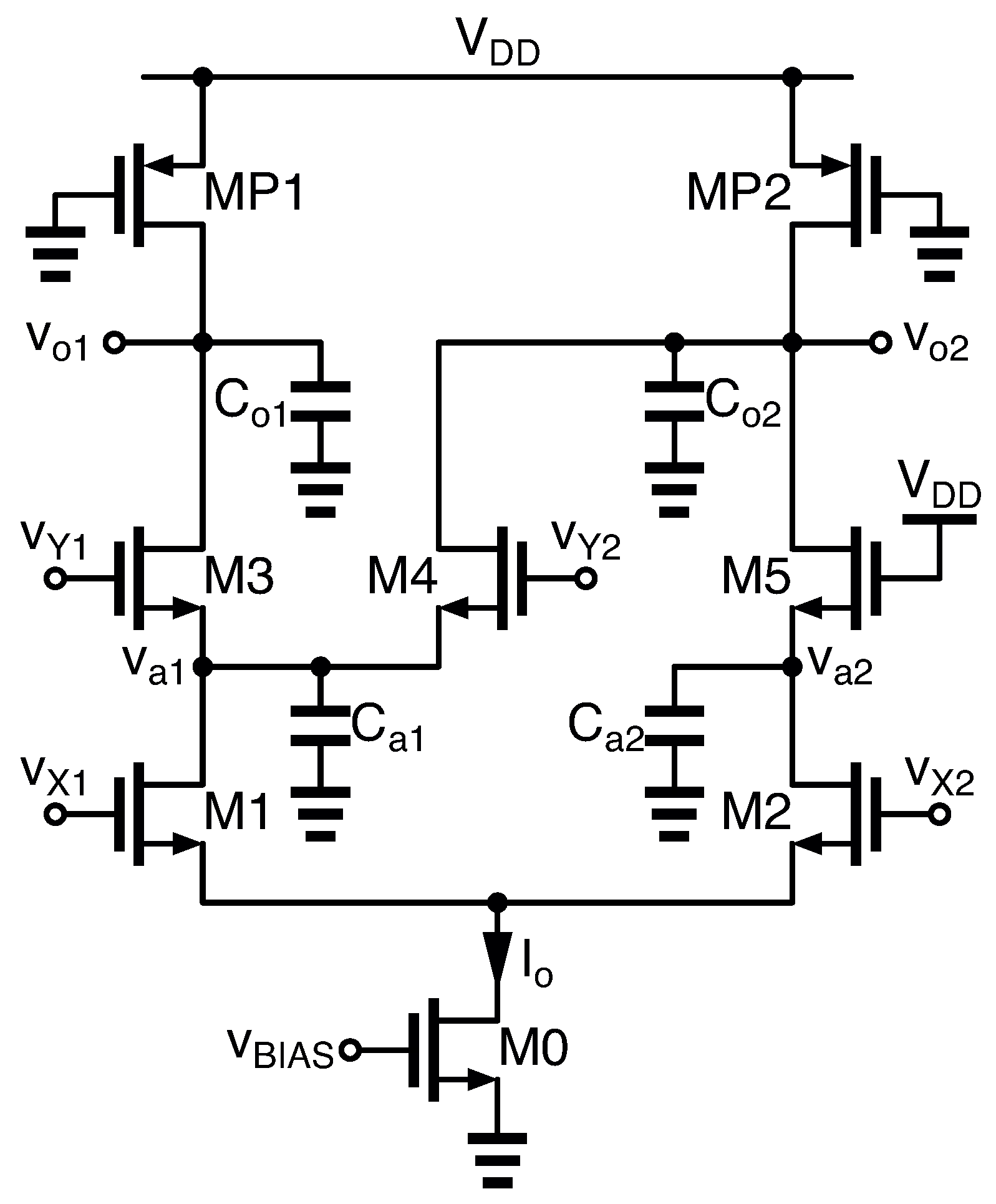
3. MCML Universal Gate Delay Model

The MCML universal gate is shown in Figure 4. It is made up of two cascaded source-coupled differential pairs. The lower differential pair, M1–M2, processes the input v X = v X 1 v X 2 , and the upper differential pair, M3–M4, processes the input v Y = v Y 1 v Y 2 . PMOS devices, MP1–MP2, are biased in the triode region and act as a resistive load. Transistor M0 provides the constant current, I o , that biases the logic gate.
The conventional MCML universal gate is designed without transistor M5, that is, with the drain terminal of M2 directly connected to the output node, V o 2 . This results in a highly unbalanced and asymmetrical logic gate. In this improved topology in Figure 4, transistor M5 is used to better balance the logic gate so that M1–M2 are subject to the same drain-source voltage. This makes the circuit more symmetrical and enhances the logic gate’s performance in high-speed applications, as reported in [15]. In the figure, C o 1 and C o 2 are the equivalent output capacitors and include both the self loading effect and the external load. C a 1 and C a 2 are the equivalent capacitors in the internal nodes of the universal gate. In general, since the universal gate is not perfectly symmetrical, we have C o 1 C o 2 and C a 1 C a 2 .
With a proper combination of its inputs and output, the logic gate can realize any two-input OR/NOR/AND/NAND logic function. Independently of the logic function, in our discussion we say that M1–M2 (M3–M4) is in the ‘H’ state when v X > 0 ( v Y > 0 ). Conversely, M1–M2 (M3–M4) is in the ‘L’ state when v X < 0 ( v Y < 0 ).
The MCML universal gate has 12 possible transitions but, as reported in Table 1, only 6 of them (T7–T12) commute the output either in the rising edge (↑) or in the falling edge (↓).
In transitions T7/T8, transistor M1 remains on and M2 remains off. The commutation affects the upper differential pair, only, and the circuit behaves as a MCML inverter with a single equivalent pole at the output nodes. These transitions are not critical because, due to the single-pole behavior, they are the fastest of the universal gate.
In transitions T9/T10, transistor M4 remains off and M3 remains on. It is now the lower differential pair that switches the bias current I o to one of the output nodes. In the process, transistors M3 and M5 act as common-gate stages. These transitions are critical since they are slower than T7/T8 because the common-gate stage introduces an extra pole.
In transitions T11/T12, no current flows through transistor M4. Indeed, when V Y 2 is low, current I o reaches MP1 through transistors M1 and M3. Conversely, when V Y 2 is high, current I o reaches MP2 through transistors M2 and M5. Since these transitions are very similar to those in T9/T10, we shall limit our analysis to these last two cases only.

3.1. Simplified Analysis of Transitions T9/T10

During transitions T9/T10, the MCML universal gate is represented as in Figure 5. Transistors M1 and M2 are considered as switches that connect the constant current I o to the charging branch and disconnect it from the other, namely the discharging branch.
For a preliminary analysis, we assume the circuit to be symmetrical so that the results found for one of the two transitions can easily be applied to the other. We shall discuss below how the results change in the asymmetrical logic gate. Moreover, we assume also a linear model so that the branches of the universal gate are represented as in Figure 6, where C a = C a 1 = C a 2 , C o = C o 1 = C o 2 , g m = g m 3 = g m 5 , and g d p = g d p 1 = g d p 2 is the equivalent drain-source conductance of PMOS transistors (we neglect the resistive contribution observed at the drain terminals of M3 and M5 because both are in common-gate configurations with high drain impedances). The charging branch of Figure 5 is modeled by Figure 6a, where current I o is a step input. The discharging branch is modeled by Figure 6b, where the initial conditions depend on the voltage swings Δ V a = I o / g m and Δ V o = I o / g d p , set by the steady-state before commutation.
In the Laplace domain, we have for the charging branch
V a , c ( s ) = 1 s 1 + s τ a I o g m
V o , c ( s ) = 1 s 1 + s τ a 1 + s τ o I o g d p
and, for the discharging branch
V a , d ( s ) = τ a 1 + s τ a I o g m
V o , d ( s ) = s τ a τ o + τ a + τ o 1 + s τ a 1 + s τ o I o g d p
τ a = C a / g m and τ o = C o / g d p being the time constants related to the inner node and the output one.
At the output nodes, the corresponding time-domain equations are
v o , c ( t ) = I o g d p 1 + exp t τ a τ o / τ a 1 + exp t τ o τ a / τ o 1
v o , d ( t ) = I o g d p exp t τ a τ o / τ a 1 exp t τ o τ a / τ o 1
so that the differential output results
v o ( t ) = ± v o , d ( t ) v o , c ( t ) = ± I o g d p 1 + 2 exp t τ a τ o / τ a 1 + 2 exp t τ o τ a / τ o 1
where the ‘+’ sign holds for transition T9 and the ‘−’ sign for transition T10.

3.2. Propagation Delay

The PD is obtained by solving v o ( t P D ) = 0 but no closed form solution exists for this equation. To find an approximate solution, assuming τ o > τ a , we normalize the variables as
y = ± v o g d p / I o x = t / τ a k = τ o / τ a > 1
and rewrite (8) as
y ( x ) = 1 + 2 exp x k 1 + 2 exp x / k 1 / k 1
Using Matlab, we find the normalized propagation delay by solving y ( x P D ) = 0 for different values of k > 1 . The plot of x P D versus k is shown in Figure 7 and reveals a quasi-linear behavior. A fitting procedure led to the empirical solution
x P D = 0.690 × k + 1.090 k ln ( 2 ) + ln ( 3 )
where the error of the last expression is less than 5.7%.
Using (9) to denormalize k and x P D leads to
t P D = τ o ln ( 2 ) + τ a ln ( 3 )
Observe that, if τ a > τ o then (12) turns into t P D = τ a ln ( 2 ) + τ o ln ( 3 ) .

3.3. Effect of the Asymmetry

The presence of transistor M4 in Figure 4 implies C o 1 C o 2 and C a 1 C a 2 . This means that the time constants of the left branch differ from the corresponding time constants of the right branch.
To analyze how the circuit behaves with asymmetrical time constants, we evaluate the signals at the output nodes considering τ a 1 τ a 2 and τ o 1 τ o 2 . During transition T10, the output signals are
v o 1 ( t ) = I o g d p 1 + exp t τ a 1 τ o 1 / τ a 1 1 + exp t τ o 1 τ a 1 / τ o 1 1
v o 2 ( t ) = I o g d p exp t τ a 2 τ o 2 / τ a 2 1 exp t τ o 2 τ a 2 / τ o 2 1
Observe that the output signals during transition T9 can be obtained by simply exchanging the subscript 1 with 2 in (13). Subtracting (13a) to (13b), we obtain the output voltage as
v o ( t ) = ± I o g d p 1 + H a ( t ) + H o ( t )
where the ‘+’ sign holds for transition T9, the ‘−’ sign for transition T10 and where
H a ( t ) = exp t τ a 1 τ o 1 / τ a 1 1 + exp t τ a 2 τ o 2 / τ a 2 1
H o ( t ) = exp t τ o 1 τ a 1 / τ o 1 1 + exp t τ o 2 τ a 2 / τ o 2 1
As demonstrated in Appendix A, H a ( t ) and H o ( t ) can be simplified as in (A3) and (A5) and the output voltage reported in (14) turns into (8) where
C a = C a 1 + C a 2 2 τ a = τ a 1 + τ a 2 2 = C a g m
C o = C o 1 + C o 2 2 τ o = τ o 1 + τ o 2 2 = C o g d p
It is worth emphasizing that, although the MCML universal gate is asymmetrical, it behaves as if it were symmetrical as long as all capacitive contributions are averaged between the two branches of the logic gate.
As a final remark, due to the above discussion, the PD is expressed by (12) where the time constants are evaluated as in (16).

3.4. Evaluating the Parameters of the Delay Model

As for the MCML inverter, this delay model is also based on the linearity assumption of the logic gate. Indeed, (12) requires the evaluation of the time constants, τ o = C o / g d p and τ a = C a / g m , where C o , C a , g d p , and g m should be small-signal parameters. However, since the universal gate works with large signals, we cannot use any small-signal parameter evaluated in a single bias point.
To maintain the delay model as simple as possibile, we use the average value over the two bias conditions that the logic gate assumes during transitions T9/T10. In particular, referring to Figure 5, and maintaining M3–M4 in the ‘H’ state, the first bias point refers to M1–M2 in the ‘H’ state and the second bias point refers to M1–M2 in the ‘L’ state. Therefore, for transconductance g m and conductance g d p , we consider
g m = g m 3 ( H ) + g m 3 ( L ) 2 = g m 5 ( H ) + g m 5 ( L ) 2
g d p = g d 1 ( H ) + g d 1 ( L ) 2 = g d 2 ( H ) + g d 2 ( L ) 2
Observe that the universal gate is symmetrical for the transistors’ transconductances and conductances so that g m 3 ( H , L ) = g m 5 ( L , H ) and g d p 1 ( H , L ) = g d p 2 ( L , H ) .
Referring to the capacitive contributions, we have to average the values between the left and the right side of the universal gate as well as the values between the ‘H’ and the ‘L’ states. Therefore, we have
C a = C a 1 ( H ) + C a 2 ( H ) 2 + C a 1 ( L ) + C a 2 ( L ) 2 2 = C a 1 ( H ) + C a 1 ( L ) + C a 2 ( H ) + C a 2 ( L ) 4
C o = C o 1 ( H ) + C o 2 ( H ) 2 + C o 1 ( L ) + C o 2 ( L ) 2 2 = C o 1 ( H ) + C o 1 ( L ) + C o 2 ( H ) + C o 2 ( L ) 4
Similarly to the MCML inverter, as we shall validate in the next section, these simplifications allow a nonlinear circuit to be treated as if it were linear, provided that its equivalent small-signal parameters are evaluated as described above.

4. Delay Model Validation and Comparison

To provide a validation of the proposed PD models, the MCML inverter gate reported in Figure 1 and the MCML universal gate shown in Figure 4 were designed using a 65-nm standard CMOS and a 28-nm FD-SOI process.

4.1. 65-nm Standard CMOS

Using the nominal supply voltage, V D D = 1.2 V, and following the design strategy in [14,32], we designed the MCML inverter and the universal gate with a nominal bias current, I o , of about 20 μ A, a differential peak-to-peak voltage swing, 2 Δ V o , of 0.8 V and transistor dimensions, as in Table 2.
For the evaluation of the PD, transistor level simulations were carried out in the Cadence Virtuoso environment referring to the test-benches reported in Figure 8a,b for the MCML inverter and the universal gate, respectively. The input terminals of the digital gate under the test are driven by the cascade of two MCML inverters which act as waveform shapers and provide realistic input waveforms. The output of the logic gate under the test is loaded by another MCML inverter which emulates a realistic load. The inverters of waveform shapers and digital load have the same aspect ratios reported in Table 2.
The PD of the MCML inverter is established in (3) and depends on the time constant associated to the output node, τ o = C o / g d p . Parameters C o and g d p are obtained from (4) using the values reported in Table 3 that were computed as detailed in Appendix B. The PD evaluated from (3) results in t P D = 12.5 ps. This theoretical value was compared to the PD computed in the transient simulations reported in Figure 9. The input signal is switched from high to low, as in Figure 9a, and back from low to high, as in Figure 9b. The inverted output signal, v o = v o 1 v o 2 , is plotted accordingly. The propagation delays result in t P D = 13.61 ps in both cases, with an error lower than 9%, thus confirming the good agreement of the proposed linearized model.
The PD of the MCML universal gate is established in (12) and depends on the time constant associated to the output node, τ o = C o / g d p , and on that associated to the internal node, τ a = C a / g m . Parameters g m , g d p , C a , and C o , are obtained from (17) and (18), using the values reported in Table 4 that were computed as detailed in Appendix B. For the two time constants, we obtained τ a = 9.66 ps and τ o = 19.78 ps so that, from (12), the PD results t P D = 24.32 ps. This theoretical value was compared to the PD computed in the transient simulations depicted in Figure 10. Specifically, Figure 10a reports the details of transition T9 while Figure 10b is focused on transition T10. In both cases, the input v Y is maintained in the ‘H’ state and is not shown. In transition T9, the simulated PD results in 23.72 ps that becomes 25.30 ps in transition T10. Considering both cases, the error is lower than ± 4 % , once again confirming the good agreement of the proposed linearized model. As a final consideration, observe that the evaluation of the PD using a single-pole approximation would lead to t P D = τ 0 ln ( 2 ) = 13.71 ps, with an error of 42 % and 46 % compared to the values simulated in transitions T9 and T10, respectively.

4.2. 28-nm FD-SOI

According to the strategy in [14,32], we designed the MCML inverter and the universal gate to operate at the nominal supply voltage of 1.0 V with a bias current, I o , of 10 μ A. The differential peak-to-peak voltage swing, 2 Δ V o , was set to 0.6 V thus leading to the transistor sizes in Table 2.
The two MCML gates were simulated in the Cadence Virtuoso environment with the test-benches shown in Figure 8a,b. The inverters of waveform shapers and the digital load are designed with the aspect ratios reported in Table 2.
For the MCML inverter, parameters C o and g d p are obtained from (4) with the values in Table 3 that were computed as detailed in Appendix B without considering parasitic junction capacitors C j d and C j s , because of the SOI process. The expected PD evaluated from (3) is t P D = 11.88 ps. With a 11.1% error, it agrees very well with the simulated PD of 10.69 ps evaluated in both the falling and the rising edges of the waveforms in Figure 11.
As far as the MCML universal gate is concerned, parameters g m , g d p , C a , and C o , are obtained from (17) and (18), using the values reported in Table 4 that were computed as detailed in Appendix B, without considering parasitic junction capacitors, C j d and C j s , because of the SOI process. The two time constants result in τ a = 5.94 ps and τ o = 16.1 ps so that, from (12), the PD results in t P D = 17.7 ps.
This value was compared to the PD carried out from the transient simulations shown in Figure 12a,b, for transitions T9 and T10, respectively. In transition T9, the simulated PD results in 18.5 ps ( 4.3 %) that becomes 21.9 ps ( 19.2 %) in transition T10. Considering both cases, the error is lower than 20 % , thus reaffirming the good agreement of the proposed linearized model. Also in this case, the evaluation of the PD using a single-pole approximation would lead to t P D = τ 0 ln ( 2 ) = 11.2 ps, with an error of 39.5 % and 49 % compared to the values simulated in transitions T9 and T10, respectively.

5. Conclusions

In this article, we have developed a simple and accurate model for evaluating the propagation delay in MCML gates. The model describes the behavior of MCML circuits in a linear fashion, despite the circuits themselves being non-linear. Indeed, we have demonstrated that a linear model can be used provided that, for each small-signal parameter, its average value calculated between the two different switching logic states is used. The proposed model was validated through simulations of MCML universal gates that were designed using modern nanometer processes. The theoretical values of the propagation delays were able to forecast the corresponding simulated values with an error lower than 4% and 20% in 65-nm standard CMOS and 28-nm FD-SOI, respectively.
As a final remark, Table 5 summarizes the properties of different approaches for estimating propagation delay in CML ports. Properties such as model complexity, number of parameters, and model accuracy are expressed qualitatively. The table shows that approaches based on small-signal models are the simplest with the fewest parameters. Among them, the proposed model is the most accurate.

Author Contributions

Conceptualization, G.G., G.S. and G.P.; Formal analysis, G.G. and G.S.; Funding acquisition, G.P.; Investigation, G.G. and G.S.; Methodology, G.G.; Supervision, G.P.; Validation, G.S.; Writing—original draft, G.G.; Writing—review and editing, G.S. and G.P. All authors have read and agreed to the published version of the manuscript.

Funding

This research was partially funded by the European Union (NextGeneration EU), through the MUR-PNRR project SAMOTHRACE (ECS00000022).

Data Availability Statement

Data available on request due to non-disclosure restrictions.

Conflicts of Interest

The authors declare no conflict of interest.

Appendix A. First Order Analysis of Asymmetrical Universal Gate

In this appendix, we demonstrate how (14) is handled to obtain a compact expression of the output voltage.
Let us express the time constants in terms of their average values and percentage deviations, that is
τ a 1 = τ a 1 ϵ a 2 τ a 2 = τ a 1 + ϵ a 2
τ o 1 = τ o 1 ϵ o 2 τ o 2 = τ o 1 + ϵ o 2
To manipulate (15a), we use (A1) and approximate
exp t τ a 1 1 ϵ a 2 t τ a exp t τ a
exp t τ a 2 1 + ϵ a 2 t τ a exp t τ a
1 τ o 1 / τ a 1 1 1 + ϵ o 2 ϵ a 2 τ o / τ a τ o / τ a 1 τ o / τ a 1
1 τ o 2 / τ a 2 1 1 ϵ o 2 ϵ a 2 τ o / τ a τ o / τ a 1 τ o / τ a 1
Substituting (A2) into (15a), and neglecting second order terms, we obtain
H a ( t ) 2 exp t τ a τ o / τ a 1
In a similar fashion, we manipulate (15b) using (A1) and approximating
exp t τ o 1 1 ϵ o 2 t τ o exp t τ o
exp t τ o 2 1 + ϵ o 2 t τ o exp t τ o
1 τ a 1 / τ o 1 1 1 + ϵ a 2 ϵ o 2 τ a / τ o τ a / τ o 1 τ a / τ o 1
1 τ a 2 / τ o 2 1 1 ϵ a 2 ϵ o 2 τ a / τ o τ a / τ o 1 τ a / τ o 1
Substituting (A4) into (15b), and neglecting second order terms, we obtain
H o ( t ) 2 exp t τ o τ a / τ o 1
The important result is that, despite the MCML universal gate being asymmetrical, it can be assumed as symmetrical provided that all the capacitive contributions are averaged between the two branches of the logic gate.

Appendix B. Equivalent Capacitors from Simulation Data

In this appendix, we discuss how to determine the equivalent capacitors of MCML gates (i.e., C a 1 , 2 and C o 1 , 2 ) from simulation data.

Appendix B.1. BSIM Model of the Channel Charge

In the BSIM MOSFET model, the channel charge is modeled through a matrix that expresses the charge variation in one terminal in terms of the voltage variations at the four terminals of the device. Specifically, we can write
d Q D d Q G d Q S d Q B = C d d C d g C d s C d b C g d C g g C g s C g b C s d C s g C s s C s b C b d C b g C b s C b b · d V D d V G d V S d V B
where the generic capacitive contribution is
C i j = Q i V j ( i , j ) { d , g , s , b }
If a terminal is connected to a fixed voltage, it does not give any contribution to the charge variation.
The capacitive matrix associated to the channel charge has the following properties
i C i j = 0 j
j C i j = 0 i
and
C i j > 0 if i = j
C i j < 0 if i j

Appendix B.2. MCML Inverter

The equivalent output capacitor of the MCML inverter can be determined referring to Figure A1, which depicts the generic half side of the stage. The output capacitor, C o 1 , 2 , includes an equivalent capacitor due to transistors’ channel charges and a capacitive contribution due to drain/source junction capacitors. The first contribution depends on the overall charge variation at the output node with respect to the signals at the terminals of transistors M1,2, MP1,2 and ML. The latter models the load due to the input transistor of the subsequent MCML inverter, I L , as in Figure 8a. Assuming all the bulk terminals biased at constant voltages (i.e., d V B = 0 ), we have
d Q o 1 , 2 = C d d 1 , 2 d V o 1 , 2 + C d g 1 , 2 d V X 1 , 2 + C d s 1 , 2 d V S 1 , 2 transistor M 1 , 2 + C d d p 1 , 2 d V o 1 , 2 transistor MP 1 , 2 + C g g L d V o 1 , 2 + C g d L d V D L + C g s L d V S L transistor ML
Figure A1. Portion of MCML inverter for determining capacitor C o .
Electronics 12 02680 g0a1
Some simplifications can be made in this equation. (1) The sources of M1,2 and ML remain almost constant during transitions; therefore, we may assume d V S 1 , 2 0 and d V S L 0 ; (2) since the digital cell has equal input/output logic swings, the input signals are equal to the output ones but inverted in sign, that is, d V X 1 , 2 d V o 1 , 2 and d V D L d V o 1 , 2 . Hence, we can write
d Q o 1 , 2 C d d 1 , 2 C d g 1 , 2 + C d d p 1 , 2 + C g g L C g d L d V o 1 , 2
where the term in parentheses is the equivalent capacitor due to transistors’ channel charges. Adding the contributions of the drain junction capacitors ( C j d ) of M1,2 and MP1,2, we obtain the final expression for C o 1 , 2
C o 1 , 2 C d d 1 , 2 + C j d 1 , 2 C d g 1 , 2 + C d d p 1 , 2 + C j d p 1 , 2 + C g g L C g d L

Appendix B.3. MCML Universal Gate

Since we are interested in transitions T9/T10, we shall refer to Figure 5. Capacitor C a 1 includes an equivalent capacitor due to transistors’ channel charges and a capacitive contribution due to drain/source junction capacitors. Referring to Figure A2, the first equivalent capacitor depends on the overall charge variation at node ‘a1’ with respect to the signals at the terminals of M1, M3 and M4. Assuming all the bulk terminals biased at constant voltages (i.e., d V B = 0 ), we can write
d Q a 1 = C d d 1 d V a 1 + C d g 1 d V X 1 + C d s 1 d V S 1 transistor M 1 + C s s 3 d V a 1 + C s g 3 d V G 3 + C s d 3 d V o 1 transistor M 3 + C s s 4 d V a 1 + C s g 4 d V G 4 + C s d 4 d V o 2 transistor M 4
Figure A2. Portion of MCML universal gate for determining capacitor C a 1 .
Electronics 12 02680 g0a2
Some simplifications can be made in this equation. (1) The gate terminals of M3 and M4 are biased at constant voltages; therefore, d V G 3 = d V G 4 = 0 ; (2) the source of M1 remains almost constant during transitions T9/T10; therefore, we may assume d V S 1 0 ; (3) capacitors C s d 3 , 4 are very small and can be neglected; (4) since g m 3 g m 1 , we have d V a 1 ( g m 1 / g m 3 ) d V X 1 d V X 1 . Hence, we can write
d Q a 1 C d d 1 C d g 1 + C s s 3 + C s s 4 d V a 1
where the term in parentheses is the equivalent capacitor due to transistors’ channel charges. Adding the contributions of the drain/source junction capacitors ( C j d , C j s ) of M1, M3 and M4, we obtain the final expression for C a 1
C a 1 = C d d 1 + C j d 1 C d g 1 + C s s 3 + C j s 3 + C s s 4 + C j s 4
Capacitor C a 2 is determined with a similar approach and results
C a 2 = C d d 2 + C j d 2 C d g 2 + C s s 5 + C j s 5
To determine capacitor C o 2 , we refer to Figure A3. The equivalent capacitor due to transistors’ channel charges depends on the overall charge variation at the output node, ‘o2’, with respect to the signals at the terminals of M4, M5, MP2 and at the terminals of the input transistor of the subsequent stage, ML, that accounts for the load. The latter is the input transistor of the load inverter, I L , in Figure 8b, which can be assumed as the transistor M1 (or M2) in the MCML inverter in Figure 1. Assuming all the bulk terminals biased at constant voltages (i.e., d V B = 0 ), we have
d Q o 2 = C d d 4 d V o 2 + C d g 4 d V G 4 + C d s 4 d V a 1 transistor M 4 + C d d 5 d V o 2 + C d s 5 d V a 2 transistor M 5 + C d d p 2 d V o 2 transistor MP 2 + C g g L d V o 2 + C g d L d V D L + C g s L d V S L transistor ML
Figure A3. Portion of MCML universal gate for determining capacitor C o 2 .
Electronics 12 02680 g0a3
In this case, we have the following simplifications. (1) The gate terminal of M4 is biased at a constant voltage, i.e., d V G 4 = 0 ; (2) capacitors C d s 4 , 5 are very small and can be neglected; (3) the source of ML remains almost constant during transitions T9/T10; therefore, we may assume d V S L 0 ; (4) since the loading inverter has equal input/output logic swings, d V D L d V o 2 . Hence, we can write
d Q o 2 C d d p 2 + C d d 5 + C g g L C g d L + C d d 4 d V o 2
where the term in parentheses is the equivalent capacitor due to transistors’ channel charges. Adding the contributions of the drain junction capacitors ( C j d ) of M4, M5 and MP2, we obtain the final expression for C o 2
C o 2 C d d p 2 + C j d p 2 + C d d 5 + C j d 5 + C g g L C g d L + C d d 4 + C j d 4
Capacitor C o 1 is determined with a similar approach and results
C o 1 = C d d p 1 + C j d p 1 + C d d 3 + C j d 3 + C g g L C g d L

References

  1. Tang, D.D.; Solomon, P.M. Bipolar Transistor Design for Optimized Power-Delay Logic Circuits. IEEE J. Solid-State Circuits 1979, SC-14, 679–684. [Google Scholar] [CrossRef]
  2. Chor, E.F.; Brunnschweiler, A.; Ashburn, P. A Propagation-Delay Expression and its Application to the Optimization of Polysilicon Emitter ECL Processes. IEEE J. Solid-State Circuits 1988, 23, 251–259. [Google Scholar] [CrossRef]
  3. Fang, W. Accurate Analytical Delay Expressions for ECL and CML Circuits and Their Applications to Optimizing High-Speed Bipolar Circuits. IEEE J. Solid-State Circuits 1990, 25, 572–583. [Google Scholar] [CrossRef]
  4. Fang, W.; Brunnschweiler, A.; Ashburn, P. An analytical maximum toggle frequency expression and its application to optimizing high-speed ECL frequency dividers. IEEE J. Solid-State Circuits 1990, 25, 920–931. [Google Scholar] [CrossRef]
  5. Konstadinidis, G.; Berger, H. Optimization of Buffer Stages in Bipolar VLSI Systems. IEEE J. Solid-State Circuits 1992, 27, 1002–1013. [Google Scholar] [CrossRef]
  6. Yang, A.; Chang, Y.H. Physical timing modeling for bipolar VLSI. IEEE J. Solid-State Circuits 1992, 27, 1245–1254. [Google Scholar] [CrossRef]
  7. Ghannam, M.; Mertens, R.; van Overstraeten, R. An Analytical for the Determination of the Transient Response of CML and ECL Gates. IEEE Trans. Electron Devices 1990, 37, 191–201. [Google Scholar] [CrossRef]
  8. Sharaf, K.; Elmasry, M. An accurate analytical propagation delay model for high-speed CML bipolar circuits. IEEE J. Solid-State Circuits 1994, 29, 31–45. [Google Scholar] [CrossRef]
  9. Harada, Y. Delay components of a current mode logic circuit and their current dependency. IEEE J. Solid-State Circuits 1995, 30, 54–60. [Google Scholar] [CrossRef]
  10. Alioto, M.; Palumbo, G. Modelling and Design Considerations on CML Gates Under High-Current Effects. Int. J. Circ. Theor. Appl. 2005, 33, 503–518. [Google Scholar] [CrossRef]
  11. Alioto, M.; Palumbo, G. Highly accurate and simple models for CML and ECL gates. IEEE Trans. Comput.-Aided Des. Integr. Circuits Syst. 1999, 18, 1369–1375. [Google Scholar] [CrossRef]
  12. Alioto, M.; Palumbo, G. Modeling and optimized design of current mode MUX/XOR and D flip-flop. IEEE Trans. Circuits Syst. II 2000, 47, 452–461. [Google Scholar] [CrossRef]
  13. Alioto, M.; Palumbo, G.; Pennisi, S. Modeling of Source Coupled Logic Gates. Int. J. Circ. Theor. Appl. 2002, 30, 459–477. [Google Scholar] [CrossRef]
  14. Alioto, M.; Palumbo, G. Power-aware design techniques for nanometer MOS current-mode logic gates: A design framework. IEEE Circuits Syst. Mag. 2006, 6, 40–59. [Google Scholar] [CrossRef]
  15. Musa, O.; Shams, M. An Efficient Delay Model for MOS Current-Mode Logic Automated Design and Optimization. IEEE Trans. Circuits Syst. I 2010, 57, 2041–2052. [Google Scholar] [CrossRef]
  16. Centurelli, F.; Scotti, G.; Trifiletti, A.; Palumbo, G. Delay models and design guidelines for MCML gates with resistor or PMOS load. Microelectron. J. 2020, 99, 104755. [Google Scholar] [CrossRef]
  17. Alioto, M.; Palumbo, G. CML and ECL: Optimized Design and Comparison. IEEE Trans. Circuits Syst. I 1999, 46, 1330–1341. [Google Scholar] [CrossRef]
  18. Alioto, M.; Palumbo, G. Design Strategy for Source Coupled Logic Gates. IEEE Trans. Circuits Syst. I 2003, 50, 640–654. [Google Scholar] [CrossRef] [Green Version]
  19. Alioto, M.; Palumbo, G. Design strategies of cascaded CML gates. IEEE Trans. Circuits Syst. II 2006, 53, 85–89. [Google Scholar] [CrossRef]
  20. Alioto, M.; Mita, R.; Palumbo, G. Design of High-Speed Power-Efficient MOS Current-Mode Logic Frequency Dividers. IEEE Trans. Circuits Syst. II 2006, 53, 1165–1169. [Google Scholar] [CrossRef]
  21. Scotti, G.; Trifiletti, A.; Palumbo, G. A Novel 0.5 V MCML D-Flip-Flop Topology Exploiting Forward Body Bias Threshold Lowering. IEEE Trans. Circuits Syst. II 2020, 67, 560–564. [Google Scholar] [CrossRef]
  22. Palumbo, G.; Scotti, G. A Multi-Folded MCML for Ultra-Low-Voltage High-Performance in Deeply Scaled CMOS. IEEE Trans. Circuits Syst. I 2020, 67, 4696–4706. [Google Scholar] [CrossRef]
  23. Centurelli, F.; Scotti, G.; Trifiletti, A.; Palumbo, G. Design of Low-Voltage Power Efficient Frequency Dividers in Folded MOS Current Mode Logic. IEEE Trans. Circuits Syst. I 2021, 68, 680–691. [Google Scholar] [CrossRef]
  24. Centurelli, F.; Scotti, G.; Palumbo, G. A Very-Low-Voltage Frequency Divider in Folded MOS Current Mode Logic with Complementary n- and p-type Flip-Flops. IEEE Trans. VLSI Syst. 2021, 29, 998–1008. [Google Scholar] [CrossRef]
  25. Kundan, J.; Hasan, S. Enhanced folded source-coupled logic technique for low-voltage mixed-signal integrated circuits. IEEE Trans. Circuits Syst. II 2000, 47, 810–817. [Google Scholar] [CrossRef]
  26. Leung, B. VLSI for Wireless Communication; Prentice Hall: Hoboken, NJ, USA, 2002. [Google Scholar]
  27. Razavi, B. Prospect of CMOS technology for high-speed optical communication circuits. IEEE J. Solid-State Circuits 2002, 37, 1135–1145. [Google Scholar] [CrossRef]
  28. Razavi, B. Design of Integrated Circuits for Optical Communications; McGraw-Hill Inc.: Boston, MA, USA, 2003. [Google Scholar]
  29. Yektaei, M.; Ghaznavi-Ghoushchi, M.B. PDP and TPD flexible MCML and MTCML ultralow-power and high-speed structures for wireless and wireline application. IEEE Trans. VLSI Syst. 2020, 28, 1782–1795. [Google Scholar] [CrossRef]
  30. Allstot, D.; Kiaei, S.; Zele, R. Analog logic techniques steer around the noise. IEEE Circuits Devices Mag. 1993, 9, 18–21. [Google Scholar] [CrossRef]
  31. Anis, M.; Allam, M.; Elmasry, M. Impact of technology scaling on CMOS logic styles. IEEE Trans. Circuits Syst. II 2002, 49, 577–588. [Google Scholar] [CrossRef]
  32. Alioto, M.; Palumbo, G. Model and Design of Bipolar and MOS Current Mode Logic: CML, ECL and SCL Digital Circuits; Springer: Dordrecht, The Netherlands, 2005. [Google Scholar]
  33. Jang, I.; Lee, Y.; Kim, S.; Kim, J. Power-Performance Tradeoff Analysis of CML-Based High-Speed Transmitter Designs Using Circuit-Level Optimization. IEEE Trans. Circuits Syst. I 2016, 63, 540–550. [Google Scholar] [CrossRef]
  34. Bai, Y.; Song, Y.; Bojnordi, M.N.; Shapiro, A.; Friedman, E.G.; Ipek, E. Back to the Future: Current-Mode Processor in the Era of Deeply Scaled CMOS. IEEE Trans. VLSI Syst. 2016, 24, 1266–1279. [Google Scholar] [CrossRef]
  35. Srivastava, P.; Yadav, R.; Srivastava, R. Robust circuit implementation of 4-bit 4-tube CNFET based ALU at 16-nm technology node. Analog Integr. Circuits Signal Process. 2021, 109, 127–134. [Google Scholar] [CrossRef]
  36. Centurelli, F.; Scotti, G.; Palumbo, G. 0.5-V Frequency Dividers in Folded MCML Exploiting Forward Body Bias: Analysis and Comparison. Electronics 2021, 10, 1383. [Google Scholar] [CrossRef]
  37. Rafiee, M.; Ghaznavi-Ghoushchi, M.B. Low-voltage and high-speed stand-alone multiple-input complex gates for error correction coding applications. Int. J. Circ. Theor. Appl. 2021, 49, 921–937. [Google Scholar] [CrossRef]
  38. Mita, R.; Palumbo, G.; Poli, M. Propagation Delay of an RC-Chain with a Ramp Input. IEEE Trans. Circuits Syst. II 2007, 54, 66–70. [Google Scholar] [CrossRef]
  39. Mita, R.; Palumbo, G. Propagation delay of an RC-circuit with a ramp input: An analytical very accurate and simple model. Int. J. Circ. Theor. Appl. 2009, 37, 987–994. [Google Scholar] [CrossRef]
  40. Rabaey, T.M. Digital Integrated Circuits—A Design Perspective; Prentice Hall: Hoboken, NJ, USA, 1996. [Google Scholar]
Figure 1. Transistor-level schematic of the MCML inverter.
Electronics 12 02680 g001
Figure 2. Small-signal equivalent representation of the MCML inverter stage during the commutation.
Electronics 12 02680 g002
Figure 3. Propagation delay versus the rise time of a ramp input in a single-pole system. The rise time and the propagation delay are normalized with respect to the time-constant of the single-pole system [38,39].
Electronics 12 02680 g003
Figure 4. Transistor-level schematic of the MCML universal gate.
Electronics 12 02680 g004
Figure 5. MCML universal gate in critical transitions T9/T10. Transistor M4 is always off and plays no active role in the commutation except for contributing to capacitances of C a 1 and C o 2 .
Electronics 12 02680 g005
Figure 6. Small-signal equivalent representation of the MCML universal gate during transitions T9/T10.
Electronics 12 02680 g006
Figure 7. Plot of the normalized propagation delay (Matlab evaluation and fitting equation).
Electronics 12 02680 g007
Figure 8. Test-benches used for simulations. Inverters are used as waveform shapers to provide realistic waveforms to the input terminal(s) of the logic gate under test. An inverter is connected to the output of the logic gate under test to provide realistic load.
Electronics 12 02680 g008
Figure 9. Transient simulation of the MCML inverter (65-nm standard CMOS process). Input and output signals are v X = v X 1 v X 2 and v o = v o 1 v o 2 , respectively.
Electronics 12 02680 g009
Figure 10. Transient simulation of the MCML universal gate (65-nm standard CMOS process). Signal v Y = v Y 1 v Y 2 is maintained high so only v X = v X 1 v X 2 and v o = v o 1 v o 2 are shown.
Electronics 12 02680 g010
Figure 11. Transient simulation of the MCML inverter (28-nm FD-SOI process). Input and output signals are v X = v X 1 v X 2 and v o = v o 1 v o 2 , respectively.
Electronics 12 02680 g011
Figure 12. Transient simulation of the MCML universal gate (28-nm FD-SOI process). Signal v Y = v Y 1 v Y 2 is maintained high so only v X = v X 1 v X 2 and v o = v o 1 v o 2 are shown.
Electronics 12 02680 g012
Table 1. Transitions of the MCML universal gate.
Transition v X v Y v o Transition v X v Y v o
T1 (LL → LH)LHT7 (HH → HL)H
T2 (LH → LL)LHT8 (HL → HH)H
T3 (LL → HL)LHT9 (HH → LH)H
T4 (HL → LL)LHT10 (LH → HH)H
T5 (LH → HL)HT11 (HH → LL)
T6 (HL → LH)HT12 (LL → HH)
Table 2. Transistors’ aspect ratios.
Transistor65-nm CMOS
W / L [nm/nm]
28-nm FD-SOI
W / L [nm/nm]
M02000/2401000/120
M1, M2, M3 *, M4 *, M5 *300/60320/30
MP1, MP2135/20580/94
* Only in the MCML universal gate.
Table 3. Simulated parameters’ values of the MCML inverter. ‘H’ and ‘L’ denote the two logic states as defined in Section 2. The third column is the corresponding average value between these two logic states.
Parameter65-nm CMOS28-nm FD-SOI
‘H’‘L’avg‘H’‘L’avg
C o 1 [fF]0.8210.9640.8930.5320.5890.561
C o 2 [fF]0.9640.8210.8930.5890.5320.561
g d p 1 [ μ S]32.3866.6349.5016.1049.3832.74
g d p 2 [ μ S]66.6332.3849.5049.3816.1032.74
Table 4. Simulated parameters’ values of the MCML universal gate. ‘H’ and ‘L’ refer to input v X and denote the two logic states as defined in Section 3. The third column is the corresponding average value between these two logic states.
Parameter65-nm CMOS28-nm FD-SOI
‘H’‘L’avg‘H’‘L’avg
C o 1 [fF]0.8330.9620.8980.4260.5180.472
C o 2 [fF]1.1641.0441.1040.6360.5430.589
C a 1 [fF]0.9680.7790.8730.5300.4330.482
C a 2 [fF]0.5690.7400.6540.3170.4110.364
g d p 1 [ μ S]35.1166.2550.6816.7649.3333.04
g d p 2 [ μ S]66.1634.9550.5548.3016.6632.98
g m 3 [ μ A/V]149.28.90079.05141.01.44071.22
g m 5 [ μ A/V]8.800149.479.101.440140.971.17
Table 5. Summary of different approaches for the estimation of the propagation delay in CML gates.
[1,2,3,4][5,6][8,9][10,11,12][17,18,19,20]This Work
TechnologyBipolarBipolarBipolarBipolarMOSMOS
StrategySensitivity analysisAverage branch currentLinear device modelSmall-signal model (1 pole)Small-signal model (1 pole)Small-signal model (2 poles)
Model complexityComplexSimpleAverageSimpleSimpleSimple
Number of parametersHighAverageAverageLowLowLow
Model accuracyAverageLowLowHighHighHigher
Disclaimer/Publisher’s Note: The statements, opinions and data contained in all publications are solely those of the individual author(s) and contributor(s) and not of MDPI and/or the editor(s). MDPI and/or the editor(s) disclaim responsibility for any injury to people or property resulting from any ideas, methods, instructions or products referred to in the content.

