1. Introduction
Leaky wave antennas (LWAs) [
1,
2,
3], as a kind of traveling wave antenna, possessing merits of high gain, beam scanning, a simple feeding structure, and low profile, attract extensive attention in the area of the radar and wireless communication system. Uniform LWA and periodic LWA are two classical types in the family of LWA. The uniform LWA, with a radiation aperture of continuous shape or non-continuous shape (sub-wavelength period), is able to radiate scanning beams covering the forward region. The periodic LWA, with periodic unit cells based on the slow-wave waveguide, can scan from the backward region to the forward region. However, the open stopband (OSB) effect is an inherent issue in the periodic LWA. In addition, with the new vitality of the artificial metamaterial technology, LWAs based on artificial metasurface were also studied in the recent decade, especially spoof surface plasmon polaritons (SSPPs)-based LWA. The reported works in [
4,
5] designed dual-band LWAs based on substrate-integrated waveguide (SIW) etched with SSPPs structure. By utilizing the high-band wave-prohibit properties and low-band radiation properties of the SIW-SSPPs structure, the two designs both perform beam-scanning properties in two different bands.
Reconfigurable LWA is able to integrate multiple performances into one set of antenna systems, which is a potential candidate for modern wireless communication. Two kinds of reconfigurable LWAs have been reported in recent years: pattern reconfigurable LWA and polarization reconfigurable LWA.
The pattern reconfigurable LWA possesses scanning beams at a fixed frequency that can be realized by varying the phase constant of the antenna at the fixed frequency. Two methods are reported. One is the binary coding way [
6,
7,
8]. A p-i-n diode serves as a binary switch with “OFF” and “ON” states controlled by the direct current (DC) bias. The “OFF” state of the p-i-n switch is marked as “0” and the “ON” state is marked as “1”. The beam direction of a p-i-n-loaded LWA varies as the coding mode, because the phase constant of the unit cell is controlled using the state of the p-i-n switch. A water-grating LWA [
8] can also be coded in a binary way to realize scanning beams at a fixed frequency. The binary switch is designed by filling the water or air in the grating boxes, considering the high dielectric constant, fluidity, and low cost of the water. The other way is by the control of DC voltage [
9,
10,
11]. The properties of beam scanning can also be realized by the change of DC voltage loading in varactors [
9], liquid crystal [
10], and graphene [
11]. The capacitance of the varactor varies with the change in the magnitude of the DC voltage, which will lead to the variation of the phase constant of the antenna. The dielectric constant of the liquid crystal or graphene also varies with the DC voltage. Then, the phase constant of the feeding waveguide filled with liquid crystal or covered with graphene also varies with the value of the DC voltage.
Except for the pattern-reconfigurable LWA, the polarization-reconfigurable LWAs were recently reported [
12,
13,
14]. In [
12], a 2-D polarization-reconfigurable holographic antenna with broadside radiation was designed, which has linear polarization (LP), right-hand circular polarization (RHCP), and left-hand circular polarization (LHCP) by utilizing a polarization-insensitive hologram as the radiating structure and an electrical-control polarization-reconfigurable feeding launcher. An LWA with RHCP and LHCP was also designed in [
13], which is a short-circuited helically slotted circular waveguide antenna. The backward and forward conical radiation for RHCP and LHCP, respectively, are leaked through the helical slit, depending on the handedness of the feed. In [
14], a spatial multi-polarized SSPP LWA was proposed, which is able to simultaneously radiate RHCP, LHCP, and LP waves in the azimuth direction by the design of orthogonal grooves of the SSPP waveguide to generate rotating electric fields. In the reconfigurable LWA area, much attention focuses on the scanning radiation patterns at the fixed frequency. A few works study the polarization-reconfigurable LWA, and these designs [
12,
13,
14] always possess the polarization diversity over a very narrow beam-scanning region or even at a fixed beam angle.
In this paper, a polarization-reconfigurable LWA is proposed based on half-mode SIW etched with an SSPPs structure (SSPPs-HSIW [
4,
5]) with CP and LP performance covering about 73°. The SSPPs-HSIW is the feeding waveguide, which has high dispersion properties compared with the SIW and SSPPs transmission line (TL). The radiation unit cell is a circular metal patch with a narrow slit loaded using a p-i-n diode at the edge. Then, the efficient radiation aperture can be changed using the state of the p-i-n diodes. The LP waves are mainly leaked through the slots printed in the circular patches as the p-i-n diodes are switched off. The CP waves are mainly radiated from the circular edges of the circular patches as the p-i-n diodes are switched on. The proposed antenna has high directivity, scanning beams, and polarization diversity, which is a feasible solution for modern wireless communication that needs a polarization division multiplexing technique and a space division multiplexing technique to enhance the capacity of the communication system based on limited frequency resources.
2. Antenna Design and Analysis
2.1. Antenna Configuration
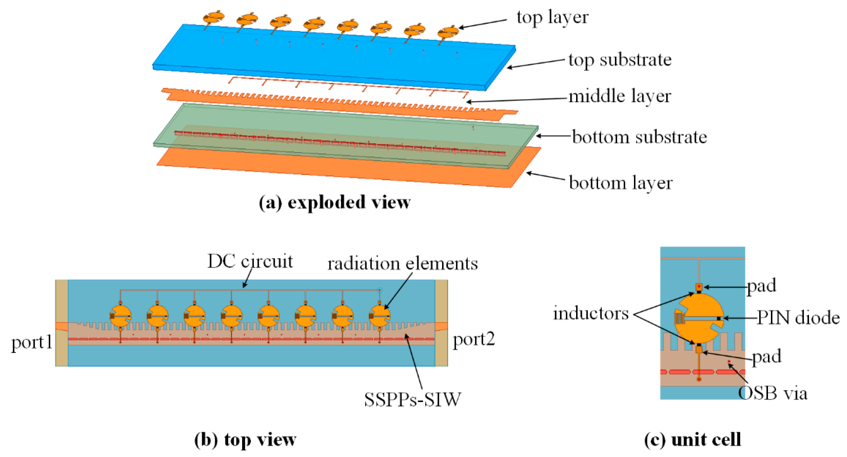
The geometry of the proposed antenna is given in
Figure 1, which consists of a transmission line at the bottom layer and radiation elements at the top layer. The two layers both utilize an F4BM265 substrate with a relative permittivity of 2.2 and loss tangent of 0.0007. The thickness of the bottom layer is 0.8 mm, and the thickness of the top substrate is 1.5 mm.
In the bottom layer, the transmission line of the proposed antenna is the SSPPs-HSIW. The period grooves are etched along the edges of the HSIW. The wide width of the HSIW is a = 5.2 mm. The period of the grooves is pl = 2 mm, and the depth of the groove is h = 2.5 mm. A set of metal vias connects the top surface to the bottom surface of SSPPs-HSIW in order to eliminate the OSB effect for the LP radiation.
In the top layer, 8 metal circular patches are periodically printed on the top surface. The radius and the periodic of the circular patches are Ra = 3.5 mm and P = 12 mm, respectively. In the unit cell, a slot with width ws = 0.5 mm symmetrically cuts the circular patch, and a p-i-n diode is loaded on the right side of the slot. A pair of inductors is utilized as an RF chock for the p-i-n diode. A pair of 50°-tilted slits is also etched in the unit cell in order to enhance the CP performance.
2.2. Transmission Line Design
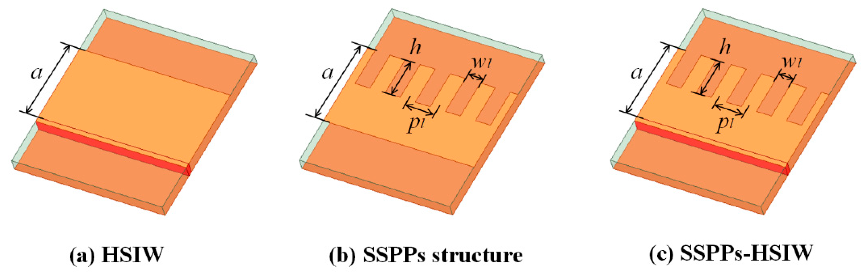
The SSPPs-SIW is utilized as the feeding line of the proposed antenna, which is composed of HSIW and microstrip SSPPs transmission line (TL). In
Figure 2, the profiles of three types of TL are given, including HSIW, SSPPs TL, and the SSPPs-HSIW. The dispersion curves of the three TLs are also given in
Figure 3.
As shown in
Figure 3, HSIW possesses high-pass properties, the cutoff frequency of which is 6.9 GHz, controlled by the width of the wide wall. The SSPPs structure has low-pass properties, the cutoff frequency of which is around 17 GHz, controlled by the depth of the grooves. Its high dispersion near the cutoff frequency is capable of tightly confining the electromagnetic waves on the surface. Then, etching the SSPPs structure along the open edge of HSIW is designed as the feeding line of the proposed antenna, which performs band-pass properties from 6.9 to 17 GHz. The dispersion properties of the designed SSPPs-HSIW are higher than the microstrip SSPPs TL and the HSIW. The influence of the depth of the grooves etched on the HSIW is studied in
Figure 4. With the increase in the depth of grooves, the dispersion curve of the designed SSPPs-HSIW moves away from the dispersion curve of the HSIW gradually. In other words, with the increase in the depth of grooves, the cutoff frequency goes lower, and the dispersion properties become higher. Overall, the higher scanning rate of LWA will be achieved by utilizing the SSPPs-HSIW as a feeding line rather than SSPPs TL or the HSIW due to the higher dispersion properties of the SSPPs-HSIW.
2.3. Radiation Element Design
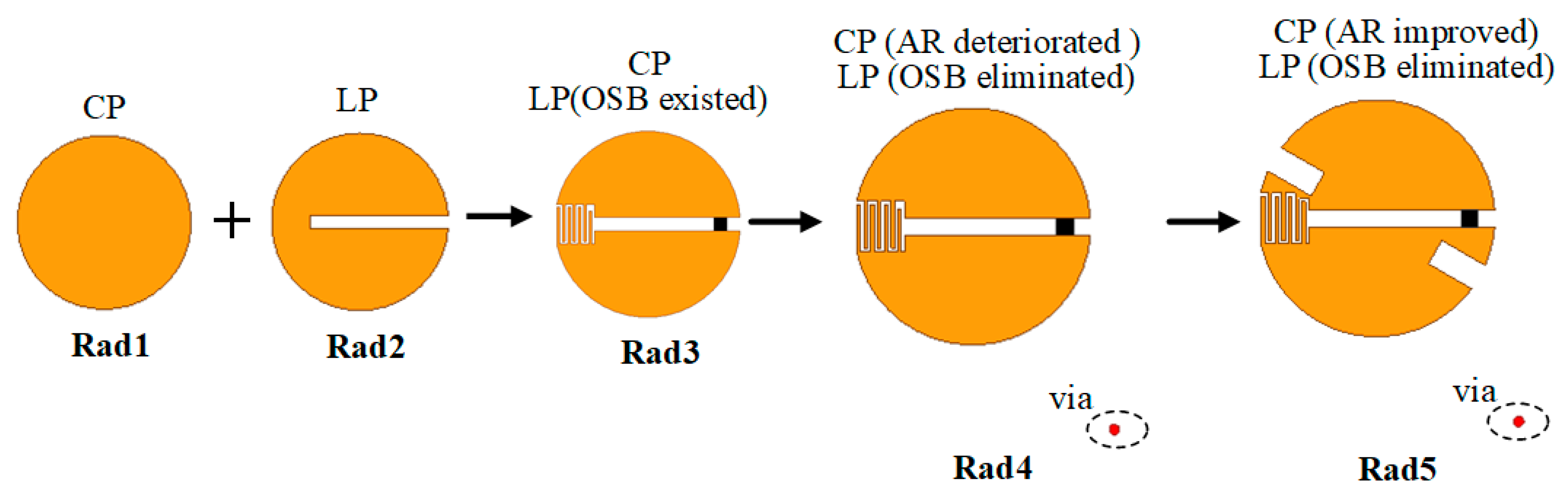
The design of the feeding waveguide for the proposed LWA is analyzed above. Then, the radiation element of the proposed antenna is designed in this section, and the design process is illustrated in
Figure 5.
The structure of “Rad1” is a circular metal patch. The proposed antenna with “Rad1” as radiation elements has CP properties. According to
Figure 6, RHCP scanning beams are realized as the guiding waves travel from port 1 to port 2. On the contrary, LHCP scanning beams are formed as the guiding waves travel from port 2 to port 1. The structure of “Rad2” is a circular metal patch printed with a straight slot. As shown in
Figure 7, the antenna with “Rad2” as radiation elements radiates scanning beams with LP. The OSB effect can be observed in
Figure 7, which shows the radiation gain at broadside frequency (11.4 GHz) obviously declines.
Then, aiming to generate the LP and CP properties in one antenna, the radiation element of “Rad3” is designed by combining the structures of “Rad1” and “Rad2”. A p-i-n diode is loaded at the right of the slot as an electronic switch. A meander slit is printed at the left of the straight slot. The meander slit performs small capacitance when an RF (radio frequency) signal goes on, and simultaneously can prohibit the DC-biased current between two half-circular patches. The performance of the AR (axial ratio) and S parameters of the antenna with “Rad3” can be observed in
Figure 8 and
Figure 9, which demonstrates good CP properties as the p-i-n diode is turned on, but an OSB effect for LP as the p-i-n diode is turned off.
In order to solve the OSB effect of LP, a structure of “Rad 4” is designed. A metal via is loaded in the SSPPs-HSIW. However, the introduction of vias will lead to AR deterioration of CP, as shown in
Figure 10. In order to further improve AR, the structure of “Rad5” is proposed. A pair of tilted slits is printed in the circular patch. The final design of the proposed radiation element is the structure of “Rad5”.
The surface current distribution on the patch at 11.4 GHz is given in
Figure 10. As the diode is switched off, the vertical current is prohibited to flow between two semicircular patches, and only a horizontal current is coupled between them. Therefore, the radiation patch has LP properties as the diode is switched off.
However, as the diode is switched on, the two semicircular patches not only can be coupled the horizontal current with each other, but also has the vertical current flowing. In addition, the two orthogonal currents have a quarter-phase shift. This demonstrates that the radiation patch radiates CP waves as the diode is switched on.
2.4. OSB Elimination and AR Improvement
For a periodic LWA with LP scanning beams, the OSB effect is an instinctive issue, which will seriously deteriorate the radiation performance around the broadside direction, if there is no precaution to take. In order to eliminate the OSB effect for the LP radiation, a set of periodic metal vias is loaded in the HSIW-SSPPs, but it will worsen the CP radiation properties. Therefore, a pair of tilted slits is printed on the circular patch to reduce the influence of vias on the CP properties.
Figure 9 analyzes the effect of matching vias and tilted slits on the matching performance of the proposed antenna with LP radiation when the diodes are switched off. Without the matching vias, the LP antenna has to suffer from the OSB effect, which performs a serious impedance mismatching around the broadside frequency point, which will lead to a severe deterioration of the radiation performance around the broadside direction, because of the inphase superposition of the reflective waves from the radiation elements. Therefore, a set of metal vias is introduced into HSIW. The reflective waves from the vias are able to counteract the reflective waves from the radiation elements. As shown in
Figure 9, |
S11| of the proposed antenna decreases from −4 to −16 dB at 11.4 GHz by loading the matching vias, which means the OSB effect is eliminated.
The matching vias can thoroughly eliminate the OSB effect of LP radiation. However, the AR properties of CP radiation become obviously worse as the matching vias are loaded, especially on the broadside frequency band from 11.2 to 11.8 GHz, as shown in
Figure 10, which is mainly caused by the reflective waves from the matching vias. Radiation elements coupled by the waves traveling through the waveguide from port 1 to port 2 radiate RHCP scanning beams. LHCP beams can also be realized while waves travel from port 2 back to port 1. Therefore, when port 1 is excited, the reflective waves from the matching vias will bring on the rise of the LHCP radiation, worsening the AR properties of RHCP radiation, even though it facilitates the OSB elimination of LP radiation. Under the premise of the elimination of OSB of LP, the perturbation of −50° tilted slits on the radiation patches is introduced to improve the AR performance of RHCP radiation. In
Figure 9 and
Figure 10, from 10.4 to 12.4 GHz, the AR reduces to less than 3 dB, and |
S11| is less than −10 dB as the tilted slits are printed and the matching vias are loaded.
The simulated realized gain (G), directivity (D), and radiation efficiency (
) of the proposed antenna are presented in
Figure 11 and
Figure 12. The radiation efficiency (
is calculated by
. As shown in
Figure 11, the radiation efficiency for CP is from 66 to 96% in the working band over 10.4~12.8 GHz. In
Figure 12, the radiation efficiency for LP is larger than 67% and the maximum value can arrive at 90% in the working band over 10.4~12.8 GHz.
3. Experiment Results
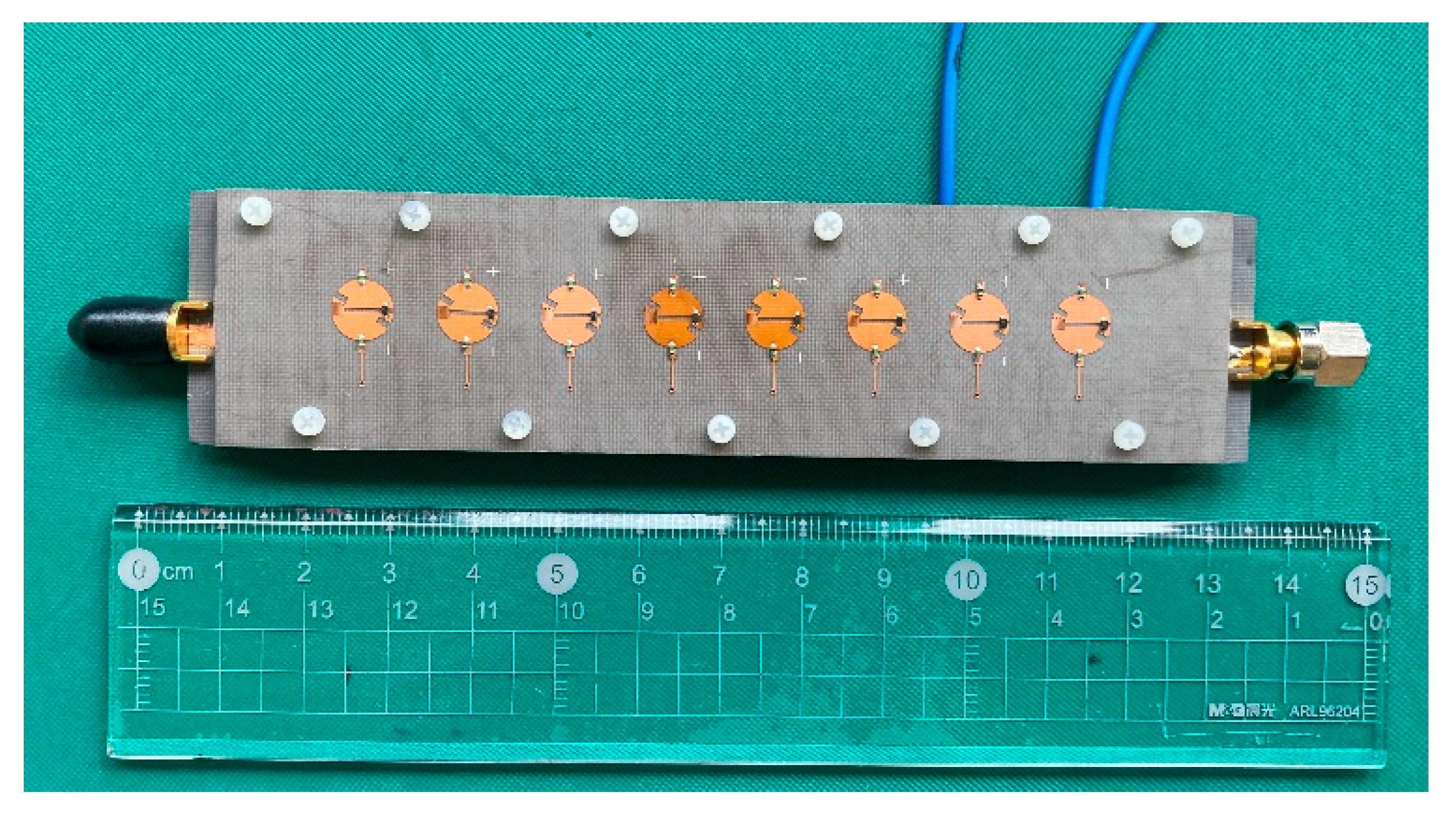
The proposed polarization-reconfigurable LWA was fabricated and experimentally studied. The prototype is shown in
Figure 13. A total of eight MADP-000907-14020 p-i-n diodes were soldered in the circular patches as electronic switches, and sixteen LQG15HS1N inductors were used to isolate the AC signal from the radiation patches to the DC circuit. The residual energy was dissipated using the 50 Ω matching loader.
The simulated and measured
S parameters of the proposed antenna are given in
Figure 14 and
Figure 15. For the CP radiation in
Figure 14, the simulated and measured |
S11| are less than −10 dB over 10~13 GHz. The simulated |
S21| is less than −7.5 dB in the working band of 10.4~12.8 GHz and the measured |
S21| is less than −12 dB over 10.6~13 GHz. The simulated and the measured results have a similar trend. The working band slightly moves toward a higher frequency, mainly due to the error of relative permittivity of the dielectric substrate. For the LP radiation in
Figure 15, the simulated and measured |
S11| are less than −10 dB over the band of 10.2~13 GHz. The simulated |
S21| is around −8 dB in the band of 10.4~12.8 GHz, and the measured |
S21| is around −12.5 dB in the band of 10.4~13 GHz. The curves of simulated |
S21| are lower than the simulated results, which is mainly attributed to the conductor and dielectric loss, as well as the loss from other RF components, such as SMA connectors, the matching loader, and lump components.
The radiation patterns of the proposed antenna for the CP and LP radiation are given in
Figure 16 and
Figure 17. When the p-i-n diodes are in the “OFF” state, the proposed antenna radiates CP beams scanning from −33° to 43°, controlled by the frequency. The simulated beams point to −33° at 10.4 GHz, −18° at 10.8 GHz, 1° at 11.4 GHz, 21° at 12.2 GHz, and 43° at 12.8 GHz. The measured beams point to −33° at 10.6 GHz, −18° at 11.0 GHz, 1° at 11.6 GHz, 19° at 12.4 GHz, and 40° at 13.0 GHz. The simulated gain fluctuates in the range from 10 to 13 dBi over the band of 10.4~12.8 GHz, and the measured gain is from 9.5 to 12.4 dBi over the band of 10.6~13 GHz. The working band of the measured results shifts toward the higher band a little more than the simulated working band, mainly because of the dielectric error of the manufactured prototype.
As the p-i-n diodes are switched on, the proposed antenna radiates LP beams scanning from −32° to 41°, including the broadside direction with the frequency varying. The simulated beams point to −32° at 10.6 GHz, −15° at 11.0 GHz, 2° at 11.6 GHz, 28° at 12.4 GHz, and 41° at 12.8 GHz. The measured beams point to −32° at 10.8 GHz, −15° at 11.2 GHz, 2° at 11.8 GHz, 25° at 12.6 GHz, and 38° at 13.0 GHz. The simulated gain fluctuates in the range from 9.9 to 13.3 dBi over the band of 10.6~12.8 GHz, and the measured gain is from 9.5 to 12.7 dBi over the band of 10.8~13 GHz. The working band of the simulated results shifts toward the higher band a little more than the simulated working band mainly because of the dielectric tolerance of the manufactured prototype.
The comparisons of the previous works and the proposed polarization-reconfigurable LWA are shown in
Table 1. As is demonstrated in
Table 1, it is worth noting that the proposed antenna has a wide scanning angle from the backward region to the forward region, including the broadside direction, while references [
12,
13,
14] have a very narrow scanning region. In addition, compared with references [
13,
14], the proposed antenna has a ground plate. Therefore, just single-beam scanning in the upper hemisphere space is beneficial to mounting the proposed antenna with the platform of the wireless communication system.
4. Conclusions
In this paper, a polarization-reconfigurable LWA is designed, which consists of SSPPs-HSIW as the main feeding waveguide and a set of periodic metal patches printed with slots and loaded with p-i-n diodes as the radiation structure. RHCP and LP performances can be switched using the state of the set of p-i-n diodes. In the “ON” state, the proposed antenna radiates RHCP waves mainly from the edges of the circular patches. In the “OFF” state, however, the proposed antenna radiates LP waves mainly from the etched slits. In order to eliminate the instinctive issue of OSB of LP beam scanning, a set of metal vias is loaded, but it will give rise to the deterioration of the CP properties in the broadside direction. Therefore, a pair of tilted slits is printed in the patch cell. The proposed antenna is able to continuously scan from −32° to 41°, including the broadside direction with LP as the p-i-n diodes are switched off and with RHCP as the p-i-n diodes are switched on. In future work, the properties of LHCP scanning beams for the proposed antenna will be further studied by improving the impedance matching of port 2.


