Article

TCAD Modeling of GaN HEMT Output Admittance Dispersion through Trap Rate Equation Green’s Functions

by
Eva Catoggio
,
Simona Donati Guerrieri
*,† and
Fabrizio Bonani
Dipartimento di Elettronica e Telecomunicazioni, Politecnico di Torino, 10129 Torino, Italy
*
Author to whom correspondence should be addressed.
These authors contributed equally to this work.
Electronics 2023, 12(11), 2457; https://doi.org/10.3390/electronics12112457
Submission received: 11 May 2023 / Revised: 24 May 2023 / Accepted: 27 May 2023 / Published: 30 May 2023
(This article belongs to the Special Issue Advanced Topics in Modelling Microwave and mmWave Electron Devices)

Abstract

:
We present a novel and numerically efficient approach to analyse the sensitivity of AC parameters to variations of traps in GaN HEMTs. The approach exploits an in-house TCAD simulator implementing the drift-diffusion model self-consistently coupled with trap rate equations, solved in dynamic conditions with the Harmonic Balance algorithm. The capability of the model is demonstrated studying the low-frequency dispersion of a 150 nm gate-length AlGaN/GaN HEMT output admittance Y DD as a function of the trap energy of Fe-induced buffer traps. The real part of Y DD exhibits strong frequency dispersion and an important degradation of the output resistance at high frequency. The imaginary part is characterized by a peak at a frequency decreasing with trap energy deeper in the gap, in agreement with experimental data on similar structures. Distributed local sources show that Y DD is most sensitive to trap energy variations localized in the buffer region under the gate, peaking under the unsaturated portion of channel towards the source. Trap variations affect the output admittance when localized in depth into the buffer up to a 100 nm distance from the channel.

1. Introduction

GaN HEMT technology is appealing for high-frequency power applications thanks to the GaN material properties, including wide bandgap and high breakdown field, good thermal management and high electron mobility [1,2]. Advanced GaN foundries on SiC [3,4,5] or Si [6] currently offer relatively mature 150 nm gate-length HEMT technologies with a portfolio of products ranging from die-level FETs to full MMIC amplifiers and circuits for microwave power applications up to 40 GHz, including space, satcom, radars and base transceiver stations for 5G. On the other hand, the development of GaN technology is still challenging in terms of reliability, cost and material quality. The multiple interfaces and material layers are still characterized by traps and defects [7,8], which ultimately limit the device performance. For example, carbon or iron buffer doping leads to acceptor-type traps [9], responsible for unwanted low-frequency dispersion of the device characteristics due to the slow trap dynamics. Such effects can be investigated with a wide range of characterization methods. Time-domain measurements are aimed at linking the trap occupation to the gate/drain current delay in response to specific stimuli such as voltage steps or pulses [10,11]. In the frequency domain, small-signal parameters [12], noise [13] or pulsed S-parameters [14,15] are used to assess the trap-related dispersion of AC and RF parameters. These techniques date back to the 1960s when silicon technology development was assisted by the AC characterization of the MOS structure in the presence of interface traps [16,17]. In experimental characterization though, it is difficult to avoid the concurrent low-frequency thermal effects due to device self-heating or to trace the detailed distribution of the traps in the device volume.
Technology CAD (TCAD) simulations have proven essential to complement measurements for the identification of GaN traps [18]. Unlike experimental characterization, TCAD simulations provide a direct link between the device terminal characteristics and the internal trap distribution and physical parameters. Furthermore, they are also important to assist the development of large signal HEMT compact models including trap dynamics, e.g., the ASM-HEMT [19], which are urgently needed to develop reliable design kits for microwave design.
It is therefore important to develop TCAD approaches that can provide fast and accurate analysis of the device performance in the presence of traps, e.g., calculating the device sensitivity to trap parameter variations. While TCAD time-domain analysis has been extensively used [2,10], frequency domain TCAD is still relatively less exploited and limited to the small-signal case.
In this contribution, we propose a novel TCAD approach, implementing the drift-diffusion model self-consistently coupled to the trap rate equations, solved in the frequency domain by means of the Harmonic Balance formulation. The simulator, extending [20,21], allows for mixed-mode device analysis in large-signal periodic and quasi-periodic conditions. A unique feature of the proposed software is that it allows for the calculation of the device Conversion Green’s Functions [22], that are used to (1) calculate the device parametric sensitivity and variability starting from a nominal “reference” device without the need for time-consuming repeated simulations with varying parameters; (2) extract the “distributed local sensitivity” to variations, i.e., a map of the internal regions of the device where variations of physical parameters most impact the device characteristics. To the author’s knowledge, this is the first demonstration of HB TCAD analysis including trap dynamics.
The capability of the model is demonstrated studying the low-frequency dispersion of a 150 nm gate-length AlGaN/GaN HEMT, varying the trap energy of Fe-induced buffer traps in the range 0.44 ÷ 0.46 eV below the conduction band. In particular, we focus on the frequency dispersion of the output impedance, which is known to be: (1) directly linked to trap dynamics and thus used for material characterization [12,18,23]; (2) especially detrimental for microwave applications in terms of higher loss, difficult matching and signal distortion in RF/baseband conversion. Both the real and imaginary parts of Y DD are analysed as a function of frequency and found to be in overall agreement with experimental data on similar structures [24]. The real part of Y DD exhibits strong frequency dispersion and an important degradation of the output resistance at high frequency. The imaginary part is characterized by a peak whose frequency decreases with increasing distance of the trap energy from the conduction band (i.e., moving deeper in the gap). We show that Y DD is most sensitive to trap energy variations localized in the buffer region below the gate, peaking under the unsaturated portion of the channel towards the source. Trap variations affect the output admittance when localized in depth into the buffer up to a 100 nm distance from the channel.

2. Trap Dynamic Model Implementation

The in-house TCAD implements the conventional drift-diffusion model coupled to a trap rate equation for each analysed trap:
· ( ϵ φ ) = q · p n + N D N A k n T , k + k δ k N T , k
n t = 1 q · J n k R n , k G n , k
p t = 1 q · J p k R p , k G p , k
n T , k t = R n , k G n , k R p , k G p , k
where φ is the electrostatic potential, n , p the electron and hole densities, J n , p the drift-diffusion current densities, and N D and N A the ionized doping concentrations. N T , k represents the total concentration of the k-th trap, while n T , k is the corresponding concentration of occupied traps. The Kronecker δ k is 0 for acceptor-like traps and 1 for donor traps. R n , p , k and G n , p , k are the recombination and generation rates due to the electron and hole trap mechanism for the k-th trap. According to the Shockley—Read—Hall theory, they are expressed as a function of the trap energy (we drop here the trap index for the sake of simplicity).
R n = N T n T c C n G n = n T   e C n
R p = n T   c V p G p = N T n T e V p
while the capture and emission rates are:
c C n = σ n v th n n   ; e C n = σ n v th n n 1
c V p = σ p v th p p   ; e V p = σ p v th p p 1
In the above expression, σ n and σ p are the trap cross sections, and v th n and v th p are the thermal velocities. The emission rates depend on the concentrations
n 1 = N C exp [ ( E T E C ) / k B T ]
and
p 1 = N V exp [ ( E V E T ) / k B T ]
where E T is the trap energy level. Fermi Dirac statics can be accounted for by simple modifications of the above expressions [25].
In the current TCAD implementation, traps are assumed to be non-interacting in terms of energy transitions and the trap rate equations are local. The extension to locally interacting traps is straightforward, defining mutual trap rates accounting for the carrier exchange among different traps [26]. Other GR mechanisms, despite being implemented in the continuity Equations (2) and (3), are not considered in this paper.
The system (1)–(4) allows to self-consistently model the effect of trap dynamics on the device electrical features. For local trap mechanisms and steady-state conditions ( n T / t = 0 ), the trap occupied density n T may be found as an analytic solution of (4), and back-substituted in the original drift-diffusion model. Despite the fact that this seems appealing from the numerical standpoint, it can be applied only in static conditions, while the substitution is not possible in many realistic device operating conditions, especially in nonlinear dynamic operation. Therefore, our TCAD tool explicitly implements the additional trap rate equations allowing for the following advantages:
  • Analysis of nonlinear dynamic operation, and in particular large-signal periodic (in our implementation through the Harmonic Balance method);
  • Straightforward extension to non-local trap mechanisms;
  • Availability of the Green’s Functions of the trap rate equations, that are useful for numerically efficient sensitivity analysis.
For a TCAD implementation, the physical model Equations (1)–(4) are discretized and converted into a system of algebraic equations which can be represented in compact form as
D ( α ) x ˙ = F ( α ) ( x , e ; σ ) α = φ , n , p , n T
where α = φ refers to the Poisson Equation (1), α = n , p to the electron and hole continuity Equations (2) and (3), and α = n T to the trap rate Equation (4) (we consider here one trap only. The generalization to several traps is straightforward). Vector σ represents the collection of the model parameters such as, e.g., trap energy, cross section, total concentration. Vector x collects the nodal values of the system unknowns (i.e., the discretized values of φ , n, p and n T ), while e represents the set of the external stimuli applied to device contacts, e.g., voltage or current sources. D ( α ) is a diagonal matrix accounting for the system memory through the time-derivatives x ˙ , while F is the memory-less part [22]. For time-varying external sources, the memory becomes important to assess the device dynamic response. For transient TCAD analysis, (11) is further discretized in the time domain and solved with generic time-varying sources e (e.g., pulses or voltage steps), but with periodic external sources, that are more adherent to the typical operating conditions in microwave stages, frequency domain analysis is better suited to describe the device. The Harmonic Balance (HB) approach was specifically developed to solve nonlinear circuits in periodic conditions, and was extended to physics-based TCAD simulations in [27]. In the TCAD HB analysis, the external sources e correspond to the superposition of DC plus harmonic stimuli with fundamental frequency ω 0 , thereby forcing the device in periodic large-signal operation. In our in-house implementation, the HB TCAD solver is further extended with the calculation of the Conversion Green’s Functions (CGFs) [22,28], allowing for fast and accurate sensitivity analysis of the device DC, AC and large-signal characteristics, along with the calculation of the corresponding local distributed variation source. We exploit this capability to carry out the sensitivity analysis of HEMT AC parameters (Y matrix) as a function of varying trap parameters.
The procedure is summarized in three steps, as illustrated in Figure 1.
  • The system (11) is converted into the frequency domain, yielding the HB system [22]
    D ( α ) Ω X = Γ F ( α ) ( Γ 1 X , E ; σ ) α = φ , n , p , n T
    where X and E are the collection of the harmonic amplitudes of x ( t ) and e ( t ) , respectively. Ω is an operator representing time derivation in the frequency domain, and Γ 1 is the operator implementing the discrete Fourier transform between phasors and time samples. In this contribution, concurrent DC and AC analyses are carried out by applying a DC voltage and a small-amplitude tone to the contacts, and calculating the corresponding phasors of the terminal currents, see Figure 1 (left). The simulation is fast, since the spectrum can be truncated to DC plus the fundamental frequency. The AC Y matrix is then recovered as
    Y q , r = I 1 ( q ) V 1 ( r )
    where V 1 ( r ) and I 1 ( q ) are the phasors of voltage at terminal r and of current at terminal q, respectively (see Figure 1, left). Notice that the admittance matrix is not based on any equivalent circuit, but rather directly stems from the solution of the physical model.
  • System (12) is linearized and the CGFs are computed with negligible numerical effort using the algorithms detailed in [22,28]. Furthermore, assuming a static parameter variation Δ σ , the microscopic local sources S α , l ( r ) are computed as the residual of (12) evaluated with the nominal solution and σ = σ 0 + Δ σ [20]. Since the parameter variation is static, the varied residual is characterized by the same spectrum of the nominal solution, as shown in Figure 1 (middle).
  • The variation of the AC terminal currents due to Δ σ is recovered by the convolution integral
    Δ I 1 ( q ) = α Ω l = 1 , 0 , + 1 G α ( q ) ( r ) ( 1 , l ) S α , l ( r ) d r
    where ( G α ( q ) ( r ) ) ( 1 , l ) is the ( 1 , l ) element of the Conversion Green’s Function.
    A graphic interpretation of the convolution is sketched in Figure 1 (right), where it is evident that (14) can be split into three individual contributions accounting for the frequency conversion effects towards the fundamental frequency. In particular, the ( 1 , 0 ) element of the Green’s Function accounts for the conversion from DC.
According to (13) and (14), the variation of the ( q , r ) element of the Y matrix is
Δ Y q , r = Δ I 1 ( q ) V 1 ( r ) = 1 V 1 ( r ) α Ω l = 1 , 0 , + 1 G α ( q ) ( r ) ( 1 , l ) S α , l ( r ) d r
The integrand function of (15), K α ( q ) ( r ) , represents the “distributed variation source” for Δ Y q , r
K α ( q , r ) ( r ) = 1 V 1 ( r ) l = 1 , 0 , + 1 G α ( q ) ( r ) ( 1 , l ) S α , l ( r ) .
In the following, we analyse the output conductance of a GaN HEMT; therefore, we will consider the particular case q = r = D , where “D” denotes the drain contact.

3. HEMT Device Structure

We consider the HEMT structure in Figure 2. The dimensions are set in line with the up-to-date technologies [23]. The gate length is 150 nm, the source-gate spacing 0.8   μ m and the drain-gate distance 2   μ m. The AlGaN barrier layer is 15 nm thick with 25% Al mole fraction, while the GaN channel region, not intentionally doped, is 5 nm thick. The 2   μ m deep GaN buffer is characterized by a residual donor doping of 10 15   cm 3 and a Fe-induced deep acceptor-like trap concentration N T = 10 18   cm 3 , nominal trap energy E T = E C 0.45 eV (being E C the conduction band edge), and electron and hole capture cross-sections σ n = σ p = 3 × 10 16 cm 2 . A fixed interface negative charge σ int with σ int / q = 2 × 10 12   cm 2 is added at the barrier/passivation interface to account for surface traps. Other details of the structure are reported in Figure 2.
The structure is simulated with the in-house TCAD software. The polarization model implemented for the GaN material system is the same as the Synopsys “Simplified strain model” [25]. GaN spontaneous polarization and both AlGaN spontaneous and piezoelectric polarization have been taken into account. The resulting net polarization charge σ pol at the AlGaN/GaN interface is such that σ pol / q = 1.34 × 10 13   cm 2 , while the polarization charge at the interface between contacts and passivation layers is supposed to be exactly compensated. The activation is set to 90% in all reported simulations.
The mobility is implemented as a function of lattice temperature (here 300 K) and total doping, according to the Sentaurus Synopsys standard models for GaN. Velocity saturation is described by the Caughey–Thomas model with v n , s a t = 2.5 × 10 7   cm / s for both AlGaN and GaN. All other material properties are in general implemented according to the standard GaN models of Sentaurus Synopsys.
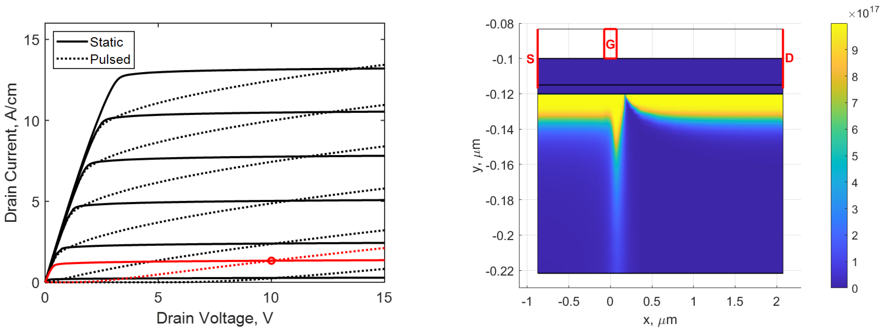
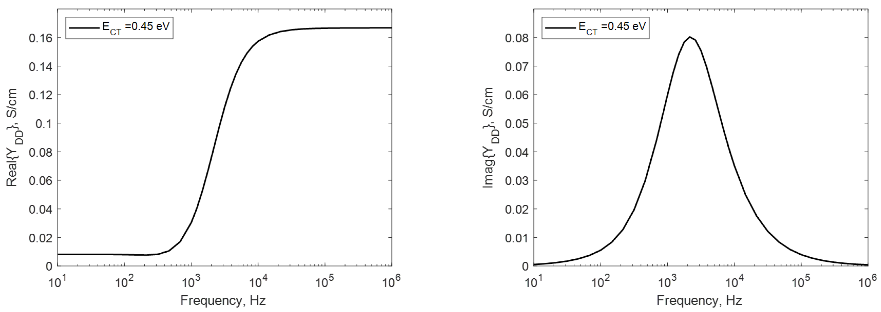
First, DC output characteristics are simulated as reported in Figure 3 (left, solid lines). The device threshold voltage is found to be V th = 2.5 V and the saturation current at V D = 10 V is I D ss = 1.3 A/mm. For the AC analysis, we select a typical bias point used in a class AB power amplifier, i.e., with a quiescent current of 10 %   I D ss , corresponding to V G = 2.22 V (red mark in Figure 3). The simulated AC Y DD parameter is shown in Figure 4 vs. frequencies varying from DC to 1 MHz: a dispersion effect is observed due to trap dynamics. This dispersion is a typical trap effect as it is due to the electrons trapped in the buffer layer, which in turn modulate the pattern of the electric field in the high field gate-drain region. This pattern is known to have an impact on the output FET resistance: at higher frequency, the trap occupancy is frozen and the output resistance differs from the low-frequency limit. The characteristic time for this phenomenon is related to the trap electron emission time τ n . The overall effect on Y DD can be recovered by an equivalent circuit [29] that predicts a Lorentzian low-frequency behavior, whose corner frequency is related to 1 / τ n [18].
The real part of Y DD is characterized by a significant increase at high frequency, corresponding to a reduction of the device output resistance R out = 1 / Real ( Y DD ) . The dispersion of the output resistance can be also observed in the simulated pulsed output characteristics, reported in Figure 3 (left, dotted lines), that show a marked change of the current slope in the saturation region. Pulsed DC simulations are readily carried out in the implemented TCAD by replacing (4) with
n T = n T 0
in each node, being n T 0 the frozen trap concentration of the quiescent bias point. For the pulsed DC curves of Figure 3, it corresponds to the same DC bias point selected for the AC analysis. The frozen trap concentration for the bias condition V D = 10 V, V G = 2.22 V is shown in Figure 3 (right). The slope of the pulsed DC curves matches the value of the real part Y DD at high frequency, while the slope of the static characteristics matches Real ( Y DD ) at low frequency. Table 1 summarizes the results obtained.
The trap signature can also be found in the imaginary part of Y DD . It exhibits a positive frequency peak at 2.15 kHz, traced back to the effect of buffer traps. The position of the peak is often investigated to identify the kind of trap and the energy level [24].

4. Sensitivity of Real ( Y DD )

As a demonstration of the potential of the implemented TCAD platform, we investigate the variation of Y DD with the trap energy, a parameter still subject to investigation as different values can be found in the literature, according to the technology and characterization method [18]. Starting from the nominal solution of the device with E T = E C 0.45 eV, we exploit the Green’s Function approach to: (1) calculate Y DD with varying E C T = E C E T in the interval 0.44 , 0.46 eV (i.e., ±10 meV) with negligible numerical effort with respect to the nominal case; (2) extract the distributed variation source (16) at each varied energy for a further insight on the impact of trap dynamics.
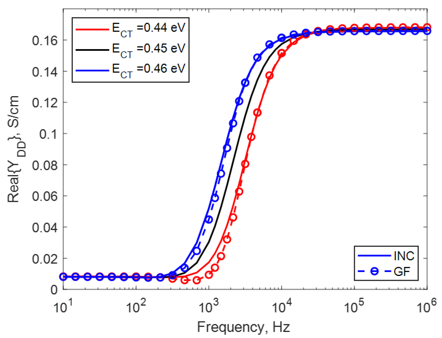
Figure 5 shows the real part of Y DD as a function of frequency. In order to validate the implemented approach, the GF analysis is compared to the Y parameters directly obtained from repeated AC analyses of (1)–(4) with varying trap energy (incremental method, INC). The accuracy is excellent and the saving in simulation time with the GF approach is remarkable (roughly 50% of the INC analysis) [30]. The values of R out at low and high frequency are practically unchanged with varying trap energy, while the frequency at which the transition occurs shifts to lower values with increasing E C T . Notice that larger E C T corresponds to a deeper trap level, hence a lower emission rate (see (7) and (8)) and, in general, higher trap occupancy.
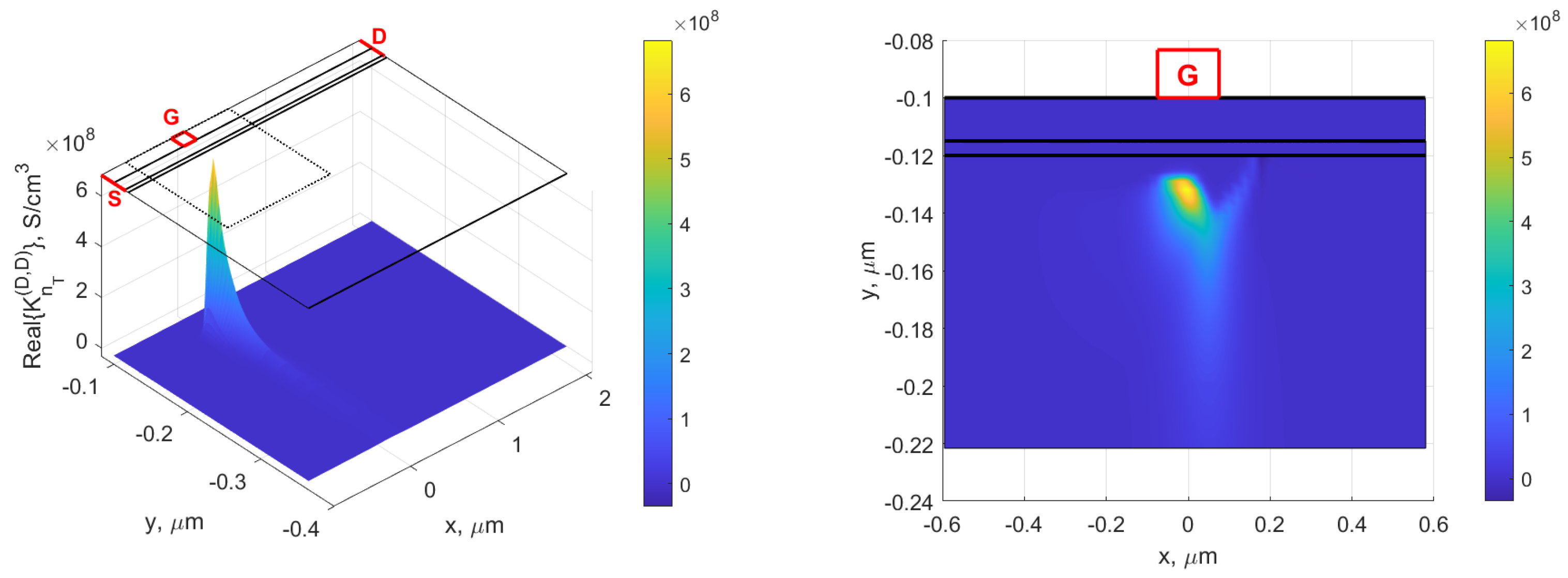
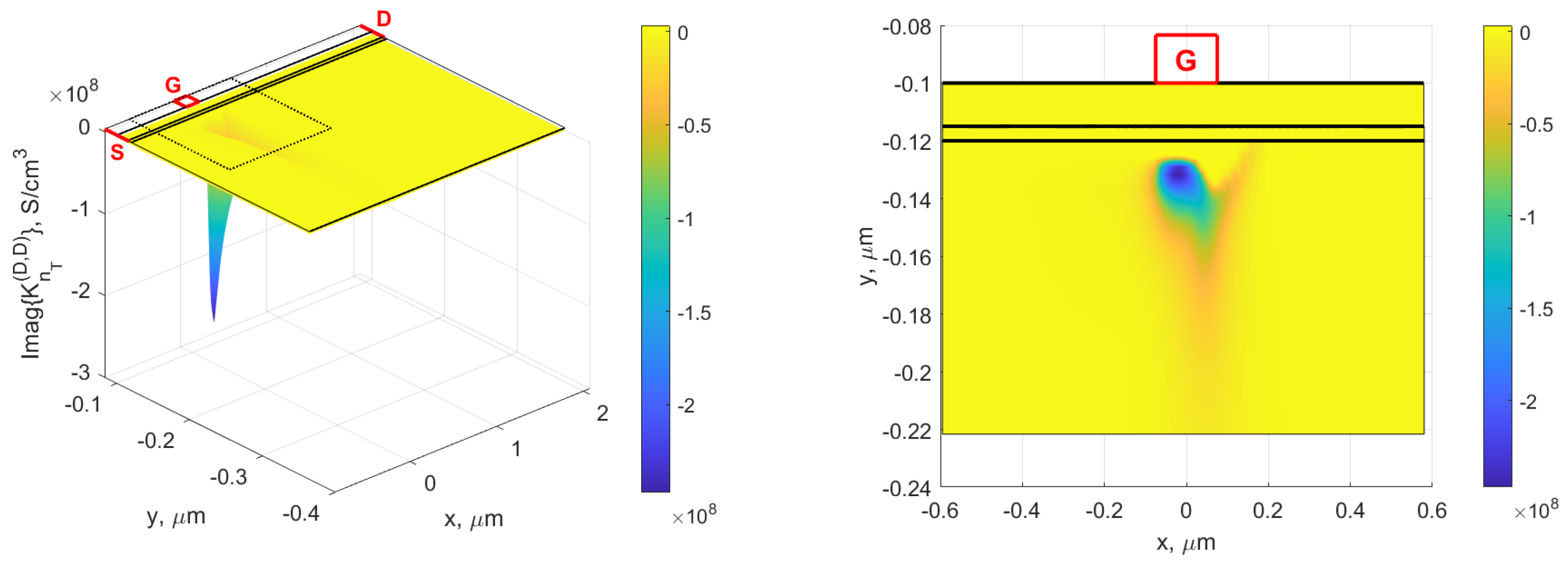
In order to grasp the mechanism giving rise to this change in the output conductance, we examine the distributed variation source (16) for a trap energy level E C T = 0.46 eV (+10 meV variation with respect to the nominal value). A preliminary inspection of the distributed local sources K α ( q , r ) ( r ) shows that the dominant one is for α = n T , i.e., only the source in the trap rate equation contributes significantly to the overall variation of Y DD . Figure 6 reports the real part of K n T ( D , D ) ( r ) at f peak = 2.15 kHz, corresponding to the frequency peak of Figure 4. Globally, the major contribution is localized below the gate, displaced approximately 10 nm from the AlGaN/GaN interface. In general, we observe that the distributed source stems from the region where trap occupation varies from fully to partially occupied. In fact, when occupancy is not complete, the occupied trap concentration n T is most affected by the variations of the trap energy. To fix the ideas on the trap occupancy portrait in the device, refer to n T with nominal E T reported in Figure 3 (right): traps are fully occupied close to the channel region, while deeper in the buffer the trap occupation drops to 10 15 cm 3 , i.e., to the value of the residual donor concentration. Below the last portion of the channel, traps are fully occupied more in depth by the injection of electrons towards the substrate due to the highly 2D pattern of the electric field, while the trap occupancy has a notch towards the drain at the exit of the saturated region of the channel. Turning back to Figure 6, the distributed variation source is found to be mainly localized below the portion of the channel extending from the source to mid-channel, where the electron velocity starts to saturate. In addition, the gate-drain regions show a contribution, being despite more limited.
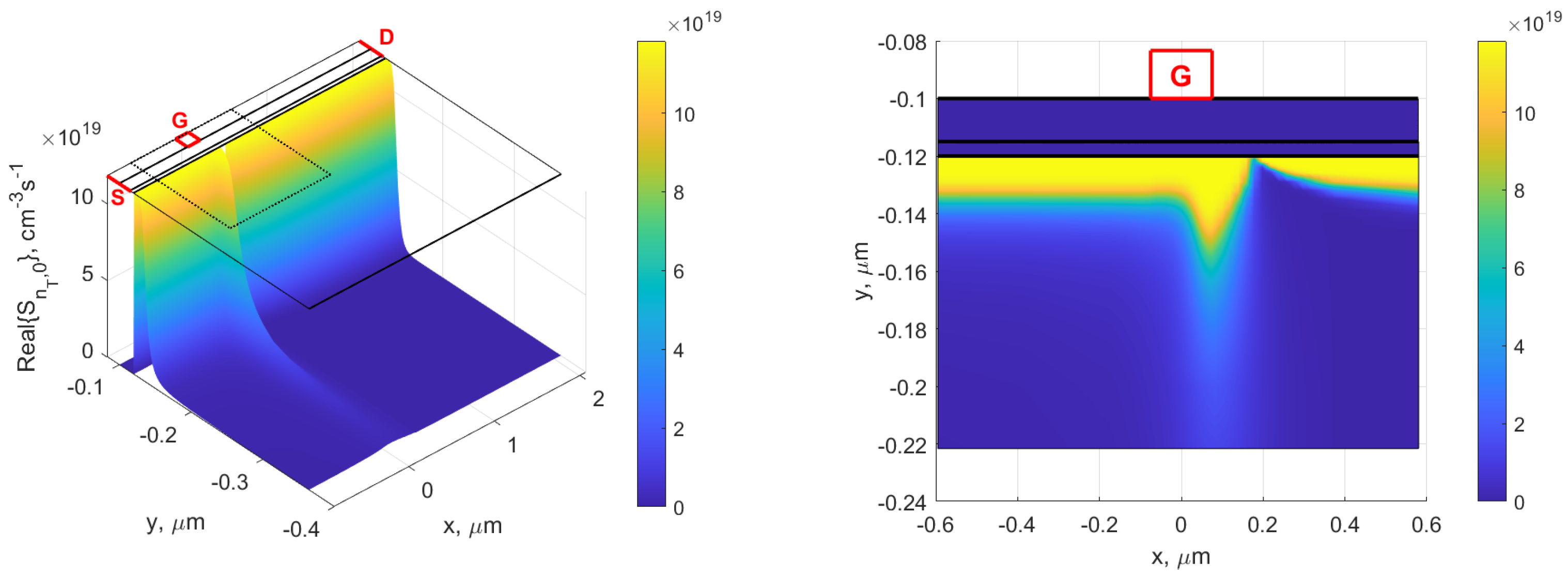
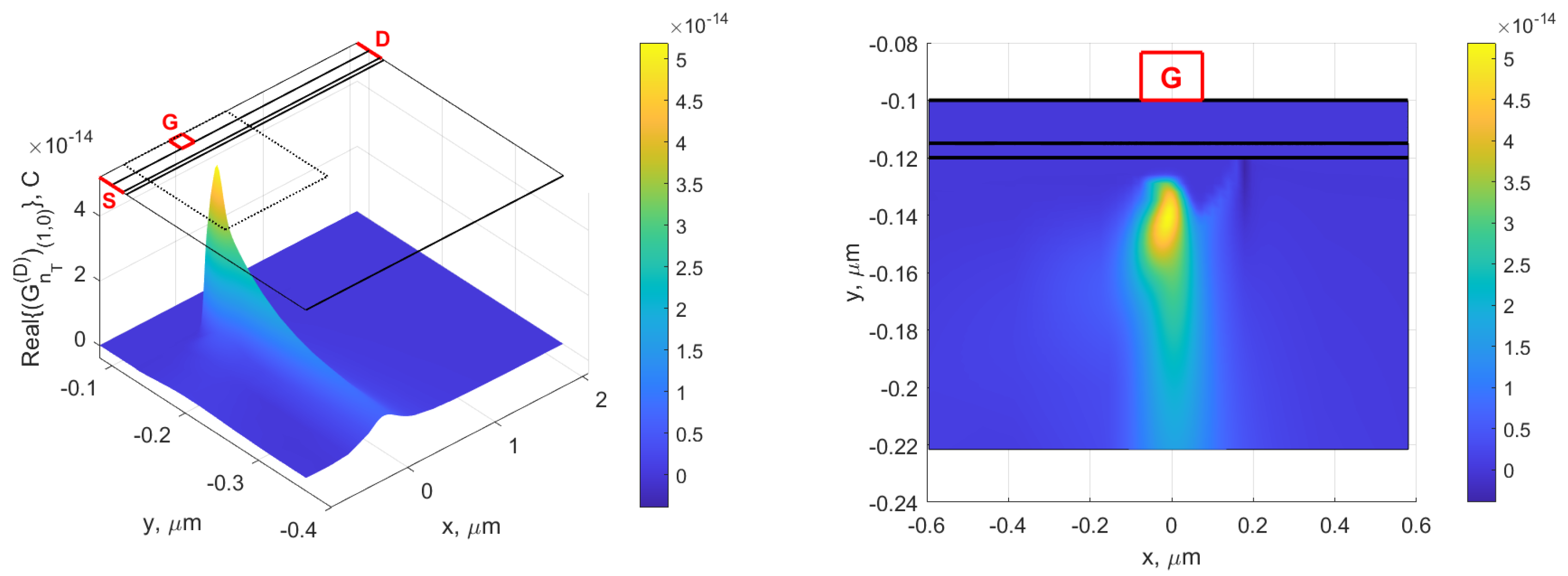
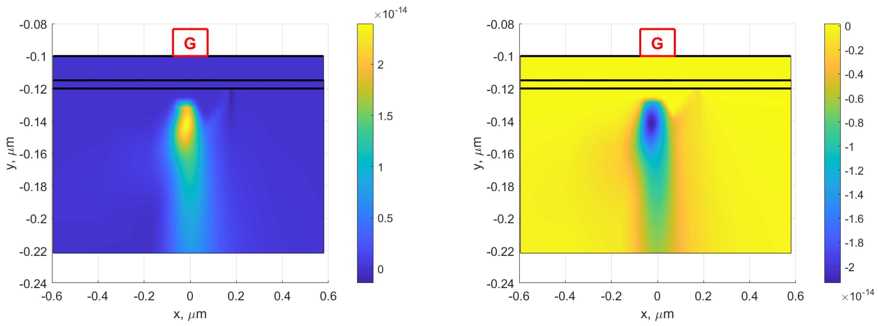
As explained in Section 2, K n T ( D , D ) ( r ) can be further split into three terms as in (16), each one composed of the product of an element of the CGF and of the local microscopic source. A detailed inspection demonstrates that the main contribution to Real ( K n T ( D , D ) ( r ) ) is given by the product of the (1,0) element G α ( D ) ( r ) ( 1 , 0 ) and of the DC component S n T , 0 ( r ) . We recall that S n T , 0 ( r ) , shown in Figure 7, is the DC component of the trap rate equation residual and essentially corresponds to the net recombination rate (5) at varied energy. Only the generation rate G n explicitly depends on E T through the emission rate (7), and it decreases with growing E T distance from the conduction band. On the contrary, the recombination rate R n is unchanged; hence, the microscopic source essentially equals the variation of the net recombination rate (5), which is, in turn, linearly dependent on the trap concentration. As a consequence, Figure 7 closely resembles the portrait of n T reported in Figure 3. On the contrary, Figure 8 shows the (1,0) component of the trap rate equation GF, which is localized under the gate, extending from source to mid-channel and approximately 40 nm in depth. Despite the fact that the velocity-saturated portion of the channel is known to affect most of the output resistance, our results show that in the presence of traps, the situation is more smeared: the last portion of the channel is not affecting Y DD significantly, but rather the source end of the channel region provides a larger contribution.

5. Sensitivity of Imag ( Y DD )

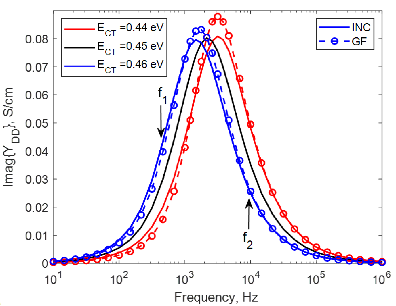
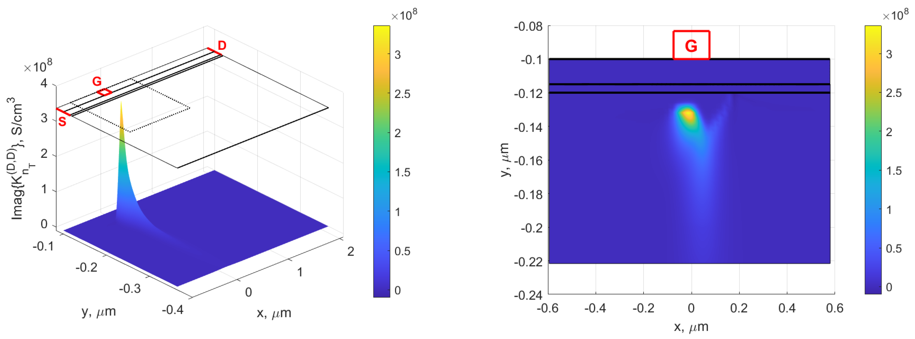
Figure 9 shows that Fe-doped traps are responsible for a positive peak at f peak 2 kHz in the imaginary part of Y DD . With decreasing E T , the peak is shifted towards higher-frequency values and Imag ( Y DD ) slightly increases. Figure 10 and Figure 11 show the imaginary part of the distributed variation source K n T ( D , D ) ( r ) for E C T = 0.46 eV for the two frequencies f 1 < f peak and f 2 > f peak defined in Figure 9. Notice that the sensitivity to E C T variations is higher at f 1 and f 2 than at the peak frequency. Similarly to the real part, the source is significant only in the buffer region below the gate. At lower frequency, the source is more concentrated at the source side of the channel and assumes positive values. At higher frequency, the local variation extends more towards the drain contact and becomes negative. Overall the portrait of Imag ( K n T ( D , D ) ( r ) ) shows that the effect of traps on the drain current (channel) is still significant when traps are located as far as 100 nm from the AlGaN/GaN interface. The highest contribution to the distributed variation is again found in the conversion from DC to AC. The DC microscopic variation source is the same reported in Figure 7. The relevant Green’s Function propagating the microscopic variations to the drain contact is the imaginary part of the (1,0) element of the trap equation GF, shown in Figure 12 for the two selected frequencies. The spatial distribution is similar to the real part case, reported in Figure 8, but is found to be more extended towards the source and deeper into the substrate at f 2 . This accounts for the extension of the local source more in depth (up to 100 nm from the channel) in the imaginary part of the output admittance.

6. Conclusions

We presented an in-house TCAD simulator implementing the trap rate equations coupled to the drift-diffusion physical model and solved in the frequency domain through the Harmonic Balance algorithm. Trap equations are solved explicitly, allowing for the extraction of the corresponding Conversion Green’s Functions, which have been presented for the time since they are not available in any commercial software.
A 150 nm gate-length Fe-doped AlGaN/GaN HEMT with buffer trap concentration of 10 18 cm 3 was used to demonstrate the software capability in the analysis of AC parameter frequency dispersion along with their dependency on the trap energy. Distributed local sources are demonstrated as valuable tools for technology optimizations, since they show the regions of the device where traps are most detrimental to the device operation.
Due to the numerical efficiency of the GF approach, the novel code opens the way to GaN HEMT variability analysis (e.g., by randomization of individual trap position, energy and cross section) without the need of computationally intensive Monte Carlo analysis.
The presented AC analysis can also be readily extended to the dynamic large-signal case with no further code variations. In particular, despite the fact that the model was presented in the case of strictly periodic inputs, the extension to the quasi-periodic case with multiple input tones at uncorrelated frequencies is straightforward. Multiple-tone analysis is the ideal framework to highlight the effect of low-frequency dispersion in microwave stages. Hence, the effect of parameter variations can be linked directly to the microwave performance of nonlinear stages in realistic operating conditions. This will be the object of future investigations.

Author Contributions

Conceptualization, methodology, and writing—review and editing, all authors; investigation, funding acquisition and writing—original draft preparation, S.D.G.; Software, E.C. All authors have read and agreed to the published version of the manuscript.

Funding

This work was supported by the Italian Ministero dell’Istruzione dell’Università e della Ricerca (MIUR) under the PRIN 2017 Project “Empowering GaN-on-SiC and GaNon- Si technologies for the next challenging millimeter-wave applications (GANAPP)”.

Data Availability Statement

The data presented in this study are available on request from the corresponding author.

Conflicts of Interest

The authors declare no conflict of interest.

References

  1. Mishra, U.; Likun, S.; Kazior, T.; Wu, Y.F. GaN-Based RF Power Devices and Amplifiers. Proc. IEEE 2008, 96, 287–305. [Google Scholar] [CrossRef]
  2. Meneghesso, G.; Verzellesi, G.; Danesin, F.; Rampazzo, F.; Zanon, F.; Tazzoli, A.; Meneghini, M.; Zanoni, E. Reliability of GaN High-Electron-Mobility Transistors: State of the Art and Perspectives. IEEE Trans. Device Mater. Reliab. 2008, 8, 332–343. [Google Scholar] [CrossRef]
  3. UMS GaN GH15-10. Available online: https://www.ums-rf.com/ums-gan-gh15-10-technology-is-space-evaluated/ (accessed on 28 May 2023).
  4. The Qorvo Gan Advantage. Available online: https://www.qorvo.com/innovation/technology/gan (accessed on 28 May 2023).
  5. MMIC Advanced Technology. Available online: https://www.winfoundry.com/en-US/Tech/tech_advanced (accessed on 28 May 2023).
  6. III—V Processes. Available online: https://www.ommic.com/iii-v-processes/ (accessed on 28 May 2023).
  7. Wang, K.; Jiang, H.; Liao, Y.; Xu, Y.; Yan, F.; Ji, X. Degradation Prediction of GaN HEMTs under Hot-Electron Stress Based on ML-TCAD Approach. Electronics 2022, 11, 3582. [Google Scholar] [CrossRef]
  8. Modolo, N.; Santi, C.D.; Minetto, A.; Sayadi, L.; Prechtl, G.; Meneghesso, G.; Zanoni, E.; Meneghini, M. Trap-state mapping to model GaN transistors dynamic performance. Sci. Rep. 2022, 12, 1755. [Google Scholar] [CrossRef] [PubMed]
  9. Joshi, V.; Soni, A.; Tiwari, S.P.; Shrivastava, M. A Comprehensive Computational Modeling Approach for AlGaN/GaN HEMTs. IEEE Trans. Nanotechnol. 2016, 15, 947–955. [Google Scholar] [CrossRef]
  10. Zagni, N.; Verzellesi, G.; Chini, A. Temperature-Independent Current Dispersion in 0.15 μm AlGaN/GaN HEMTs for 5G Applications. Micromachines 2022, 13, 2244. [Google Scholar] [CrossRef] [PubMed]
  11. Angelotti, A.M.; Gibiino, G.P.; Santarelli, A.; Florian, C. Experimental Characterization of Charge Trapping Dynamics in 100-nm AlN/GaN/AlGaN-on-Si HEMTs by Wideband Transient Measurements. IEEE Trans. Electron Devices 2020, 67, 3069–3074. [Google Scholar] [CrossRef]
  12. Oishi, T.; Otsuka, T.; Tabuchi, M.; Yamaguchi, Y.; Shinjo, S.; Yamanaka, K. Bias Dependence Model of Peak Frequency of GaN Trap in GaN HEMTs Using Low-Frequency Y22 Parameters. IEEE Trans. Electron Devices 2021, 68, 5565–5571. [Google Scholar] [CrossRef]
  13. Vertiatchikh, A.; Eastman, L. Effect of the surface and barrier defects on the AlGaN/GaN HEMT low-frequency noise performance. IEEE Electron Device Lett. 2003, 24, 535–537. [Google Scholar] [CrossRef]
  14. Beleniotis, P.; Schnieder, F.; Chevtchenko, S.; Rudolph, M. Localization of Trapping Effects in GaN HEMTs with Pulsed S-parameters and Compact Models. In Proceedings of the 2022 17th European Microwave Integrated Circuits Conference (EuMIC), Milan, Italy, 26–27 September 2022; IEEE: Piscataway, NJ, USA, 2022. [Google Scholar] [CrossRef]
  15. Gomes, J.L.; Nunes, L.C.; Pedro, J.C. Transient Pulsed S-Parameters for Trapping Characterization. In Proceedings of the 2020 International Workshop on Integrated Nonlinear Microwave and Millimetre-Wave Circuits (INMMiC), Cardiff, UK, 16–17 July 2020; IEEE: Piscataway, NJ, USA, 2020. [Google Scholar] [CrossRef]
  16. Nicollian, E.H.; Goetzberger, A. MOS Conductance Technique For Measuring Surface State Parameters. Appl. Phys. Lett. 1965, 7, 216–219. [Google Scholar] [CrossRef]
  17. Nicollian, E.; Goetzberger, A.; Lopez, A. Expedient method of obtaining interface state properties from MIS conductance measurements. Solid-State Electron. 1969, 12, 937–944. [Google Scholar] [CrossRef]
  18. Subramani, N.K. Physics-Based TCAD Device Simulations and Measurements of GaN HEMT Technology for RF Power Amplifier Applications. Ph.D. Dissertation, University of Limoges, Limoges, France, 2017. Available online: https://tel.archives-ouvertes.fr/tel-01702325 (accessed on 28 May 2023).
  19. Shanbhag, A.; Sruthi, M.P.; Chakravorty, A.; DasGupta, N.; DasGupta, A. Compact Modeling of Static and Transient Effects of Buffer Traps in GaN HEMTs. IEEE Trans. Electron Devices 2022, 69, 999–1005. [Google Scholar] [CrossRef]
  20. Donati Guerrieri, S.; Bonani, F.; Bertazzi, F.; Ghione, G. A Unified Approach to the Sensitivity and Variability Physics-Based Modeling of Semiconductor Devices Operated in Dynamic Conditions—Part I: Large-Signal Sensitivity. IEEE Trans. Electron Devices 2016, 63, 1195–1201. [Google Scholar] [CrossRef]
  21. Donati Guerrieri, S.; Bonani, F.; Bertazzi, F.; Ghione, G. A Unified Approach to the Sensitivity and Variability Physics-Based Modeling of Semiconductor Devices Operated in Dynamic Conditions.—Part II: Small-signal and Conversion Matrix Sensitivity. IEEE Trans. Electron Devices 2016, 63, 1202–1208. [Google Scholar] [CrossRef]
  22. Bonani, F.; Donati Guerrieri, S.; Ghione, G.; Pirola, M. A TCAD approach to the physics-based modeling of frequency conversion and noise in semiconductor devices under large-signal forced operation. IEEE Trans. Electron Devices 2001, 48, 966–977. [Google Scholar] [CrossRef]
  23. Raja, P.V.; Subramani, N.K.; Gaillard, F.; Bouslama, M.; Sommet, R.; Nallatamby, J.C. Identification of Buffer and Surface Traps in Fe-Doped AlGaN/GaN HEMTs Using Y21 Frequency Dispersion Properties. Electronics 2021, 10, 3096. [Google Scholar] [CrossRef]
  24. Potier, C.; Martin, A.; Campovecchio, M.; Laurent, S.; Quere, R.; Jacquet, J.C.; Jardel, O.; Piotrowicz, S.; Delage, S. Trap characterization of microwave GaN HEMTs based on frequency dispersion of the output-admittance. In Proceedings of the 2014 9th European Microwave Integrated Circuit Conference, Rome, Italy, 6–7 October 2014; IEEE: Piscataway, NJ, USA, 2014. [Google Scholar] [CrossRef]
  25. Synopsys Sentaurus. Available online: https://www.synopsys.com/silicon/tcad/device-simulation/sentaurus-device.html (accessed on 28 May 2023).
  26. Bonani, F.; Ghione, G. Noise in Semiconductor Devices; Springer: Berlin/Heidelberg, Germany, 2001. [Google Scholar]
  27. Troyanovsky, B.; Yu, Z.; Dutton, R.W. Large Signal Frequency Domain Device Analysis Via the Harmonic Balance Technique. In Simulation of Semiconductor Devices and Processes; Springer: Vienna, Austria, 1995; pp. 114–117. [Google Scholar] [CrossRef]
  28. Donati Guerrieri, S.; Pirola, M.; Bonani, F. Concurrent Efficient Evaluation of Small-Change Parameters and Green’s Functions for TCAD Device Noise and Variability Analysis. IEEE Trans. Electron Devices 2017, 64, 1269–1275. [Google Scholar] [CrossRef]
  29. Golio, J.; Miller, M.; Maracas, G.; Johnson, D. Frequency-dependent electrical characteristics of GaAs MESFETs. IEEE Trans. Electron Devices 1990, 37, 1217–1227. [Google Scholar] [CrossRef]
  30. Donati Guerrieri, S.; Ramella, C.; Catoggio, E.; Bonani, F. Bridging the Gap between Physical and Circuit Analysis for Variability-Aware Microwave Design: Modeling Approaches. Electronics 2022, 11, 860. [Google Scholar] [CrossRef]
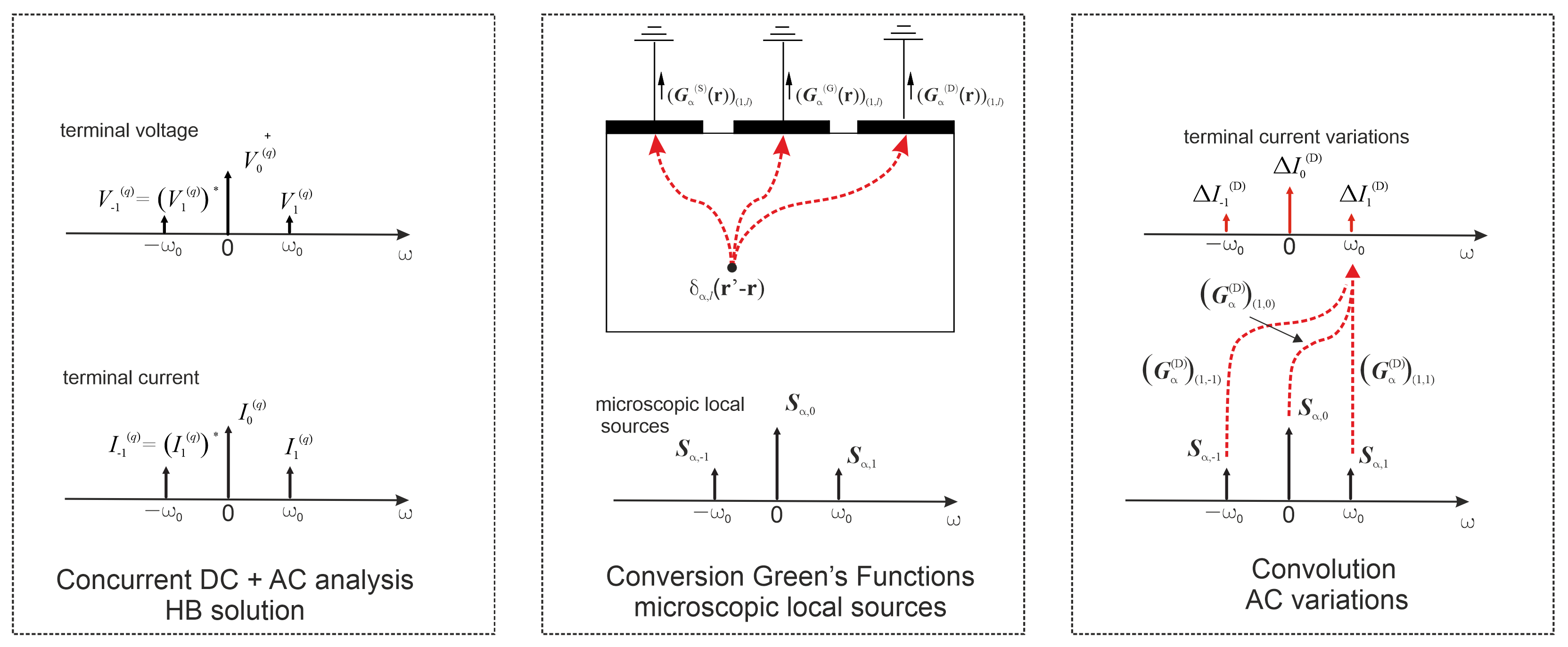
Figure 1. Graphic representation of the sensitivity analysis through Conversion Green’s Functions. Left: step 1. Middle: step 2. Right: step 3.
Electronics 12 02457 g001
Figure 2. Simulated HEMT structure.
Electronics 12 02457 g002
Figure 3. (Left) static (solid) and pulsed (dotted) output characteristics. Black lines correspond to V G from varying from −2.5 V to 0 V with 0.5 V step. The red line corresponds to V G = 2.2 V. The quiescent bias point used for pulsed simulations is shown by the red dot. (Right) occupied trap density in the bias point.
Electronics 12 02457 g003
Figure 4. Real (left) and Imaginary (right) part of Y DD with nominal energy E T = E C 0.45 eV and bias point shown in Figure 3.
Electronics 12 02457 g004
Figure 5. Real part of Y DD with varying trap energy levels. Lines: AC analysis from (1)–(4). Symbols: GF approach.
Electronics 12 02457 g005
Figure 6. (Left) 3D plot of the real part of the distributed variation source K n T ( D , D ) ( r ) at f peak = 2.15 kHz. (Right) Zoom on the dotted region under gate.
Electronics 12 02457 g006
Figure 7. (Left) 3D plot of the real part of the DC microscopic local source S n T , 0 ( r ) at f peak = 2.15 kHz. (Right) Zoom on the dotted region under gate.
Electronics 12 02457 g007
Figure 8. (Left) 3D plot of the (1,0) component of the trap rate equation Green’s Function G n T ( D ) ( r ) ( 1 , 0 ) (real part) at f peak = 2.15 kHz. (Right) Zoom on the dotted region under gate.
Electronics 12 02457 g008
Figure 9. Imaginary part of Y DD at different trap levels. Lines: INC approach. Symbols: GF approach.
Electronics 12 02457 g009
Figure 10. (Left) 3D plot of the imaginary part of distributed variation source K n T ( D , D ) ( r ) at f 1 = 464 Hz. (Right) Zoom on the dotted region under gate.
Electronics 12 02457 g010
Figure 11. (Left) 3D plot of the imaginary part of the distributed variation source K n T ( D , D ) ( r ) at f 2 = 10 kHz. (Right) Zoom on the dotted region under gate.
Electronics 12 02457 g011
Figure 12. 2D plot of the (1,0) component of the trap rate equation Green’s Function G n T ( D ) ( r ) ( 1 , 0 ) (imaginary part). (Left) f 1 = 464 Hz. (Right) f 2 = 10 kHz.
Electronics 12 02457 g012
Table 1. Summary of R out calculation.
Real ( Y DD ) [S/cm] R out [ Ω cm]
Static DC 8.2 × 10 3 122
AC Real ( Y DD ) (low frequency) 8.1 × 10 3 124
Pulsed DC0.176
AC Real ( Y DD ) (high frequency)0.176
Disclaimer/Publisher’s Note: The statements, opinions and data contained in all publications are solely those of the individual author(s) and contributor(s) and not of MDPI and/or the editor(s). MDPI and/or the editor(s) disclaim responsibility for any injury to people or property resulting from any ideas, methods, instructions or products referred to in the content.