Article

Low Leakage Current Metal–Insulator–Metal Device Based on a Beryllium Oxide Insulator Created by a Two-Step Spin-Coating Method as a Novel Type of Modified Pechini Synthesis

1
Center for Applied Electromagnetic Research, Advanced Institute of Convergence Technology, Seoul National University, Suwon 16229, Republic of Korea
2
School of Integrative Engineering, Chung-Ang University, Seoul 06911, Republic of Korea
3
Department of Chemical and Biological Engineering, Sookmyung Women’s University, Seoul 04310, Republic of Korea
*
Authors to whom correspondence should be addressed.
These authors contributed equally to this work.
Electronics 2023, 12(1), 47; https://doi.org/10.3390/electronics12010047
Submission received: 28 November 2022 / Revised: 7 December 2022 / Accepted: 8 December 2022 / Published: 23 December 2022
(This article belongs to the Section Electronic Materials)

Abstract

:
Beryllium oxide (BeO) is considered to be an attractive alternative material for use in future industries in areas such as semiconductors, spacecraft, aircraft, and rocket technologies due to its high bandgap energy, useful melting point, good thermal conductivity, and dielectric constants. In this context, our approach is a novel method to produce BeO thin films based on a two-step spin-coating innovation of the conventional powder synthesis method. The surface morphology and the crystal structure of BeO thin films were observed to be dependent on the citric acid/beryllium sulfate ratio and the sintering temperature, respectively. To characterize the BeO films, X-ray photoelectron spectroscopy was conducted for an elemental analysis. Furthermore, the bandgap of the BeO thin films was determined by reflection electron energy loss spectroscopy. Finally, the leakage current of a planar metal–insulator–metal device consisting of Au/Ti/BeO thin film/Ti/Au electrodes was determined to be below the nA range over the linear voltage sweeping range of −20 V to +20 V. These results can assist researchers in the areas of morphology control strategies, phase transfer theories, and applications that utilize BeO thin film manufactured by a solution process.

1. Introduction

Recently, ceramic materials have been spotlighted for future electric and mobile applications such as power semiconductors, electronics, automobiles, aircraft, and spaceships due to their high thermal endurance, good mechanical strength, and chemical stability. Among such candidates, beryllium oxide (BeO) has the second-highest thermal conductivity, after diamond, and significant insulating properties [1,2,3,4]. Its high thermal conductivity of 330 W/K·m originates from a smaller number of soft phonon modes due to the similarity in size between Be and O atoms [5]. The dielectric constant of BeO is 6.8 in the wurtzite structure, and its bandgap energy of 7.9 eV~10.7 eV is the highest value among the high-k dielectrics; the dielectric constant can theoretically reach 275 in rock-salt-structured BeO [6,7,8].
Despite the great potential of BeO for thermal and dielectric applications, as mentioned above, research on utilizing and engineering certain characteristics of this material has remained scant since the fundamental studies were conducted in the early 1900s [8,9,10,11,12]. Be compounds are used in three main forms, specifically Be metal, Be alloys (Cu/Be), and BeO. These pose health hazards to the skin and can cause long-term lung disease under high and repeated exposure [13,14]. Nevertheless, sintered BeO is a stable ceramic in extreme conditions, meaning that it can be utilized in spacecraft and rocket nozzle applications and as a transparent protective layer on mirrors. While BeO is a notable heat spreader and electrical insulator, for electrical applications, it is used in many high-performance semiconductor parts for applications such as a thermal sink between the silicon chips and as an interfacial layer for the metal mounts used in relation to packaging applications.
The most common method used to produce sintered BeO is the Pechini method. Pechini synthesis has successfully been adapted to 100 different mixed oxide compounds, including perovskite powders and metal oxide films, since the method was introduced by Maggio Paul Pechini in 1967 [15]. The main steps of Pechini synthesis to prepare the precursors involved in chemical reactions are chelation between complex cations and citric acid (CA) and the polyesterification of excess hydroxycarboxylic acid with glycol in a slightly acidified solution. After the two main chemical reactions, a viscous liquid is produced, increasing the covalent network trapping of metal ions in ethylene glycol (polyesterification). The residual solvent of the precursor, which does not participate in the chemical reaction, is evaporated to a form gel ceramic powder (or film), with calcination then eliminating all organic substances to deliver the final products. Otherwise, pulverization is required to break down the agglomerates in the final powders that form during the charring and calcination steps [16,17]. However, limitations of conventional Pechini techniques include a lack of thickness and lack of texture controls for the thin film process due to the viscosity of the gel precursor and the inhomogeneous nucleation that occurs during polyesterification and sintering, respectively. Although several studies have attempted to improve Pechini thin films, most approaches attempt to control the stabilization of the precursors or focus on the removal of impurities and on secondary effects during the high heat treatment, as the main highlights of the Pechini method are gelation mechanisms to ensure a high-quality powder procedure [18].
Hence, we developed a conventional modified Pechini synthesis approach for the growth of thin films of BeO realized through an innovative procedure. For the quantitative management of a sol–gel film, sequential polyesterification is used to spread an EG solution onto a substrate, after which a Be citrate solution is deposited onto the EG to synthesize a fine sol–gel film via a two-step spin-coating method. Subsequently, the textures of the BeO thin films manufactured by the two-step spin-coating method are characterized by a scanning electron microscope (SEM). The surface morphologies of the BeO layer are observed depending on the polyesterification condition with EG and the CA/beryllium sulfate (BeSO4) ratios and sintering temperatures. For an analysis of the crystal structure and the atomic binding energy of BeO, X-ray diffraction (XRD) and X-ray photoelectron spectroscopy (XPS) are conducted. Furthermore, the bandgap of BeO thin films according to the processing conditions can be determined by means of reflection electron energy loss spectroscopy (REELS). Consequently, we used the leakage of a lateral structured metal–insulator–metal (MIM) device to investigate the insulating property of the BeO thin film (Au/Ti/BeO/Ti/Au). The leakage current was held below 90 pA over linear sweeping of the applied voltage between −20 and 20 V due to the high crystallinity of the BeO thin film created through the novel modified Pechini method.

2. Materials and Methods

2.1. Modified Pechini Synthesis by Spin-Coating [19]

C-plane sapphire substrates were cleaned sequentially in acetone, methanol, and D.I. water for 20 min each using an ultrasonic bath (Power Sonic 505, Hwashin Technology, Seoul, Republic of Korea), after which they were dried using high-purity N2 (99.9%) gas. The C-plane sapphire substrates were activated by a plasma cleaner (PDC-32G, Harrick Plasma, Ithaca, NY, USA). A metallic citrate solution was prepared by dissolving beryllium sulfate (BeSO4) and citric acid (CA) in DI water and stirred to create a homogenous solution. The molar ratios of CA and BeSO4 were varied at 0.5:1, 1:1, 2:1, and 3:1. The EG was spin-coated onto the sapphire substrates at 2000 rpm for 45 s, and the Be citrate solution was then dropped and polymerized onto the deposited EG with a hot plate at 60 °C for 90 s. The sol–gel film was immediately spin-coated at 2000 rpm after polyesterification on the substrate to become a fine sol–gel film. The fine sol–gel film was annealed on the hot plate at 120 °C for 20 min to remove any residual solvent and the EG. After the soft baking process, the substrate was oxidized at 800 °C, 1100°C, 1300 °C, and 1500 °C with a 5 °C/min ramping rate for three hours using a muffle furnace (S-BA1800/Hantech, Hansen Technologies, Commerce, GA, USA).

2.2. Characterization of BeO Thin Films

Field-emission SEM (FE-SEM) was used to observe the morphologies of the various BeO layers and sapphire substrates under a 10 kV condition via Pt sputtering with an optional energy-dispersive spectrometer (EDS) (S–4800, Hitachi, Fukuoka, Japan). The structures of the BeO thin films were investigated by XRD with a zero-background aluminum disk (Empyrean, Malvern Panalytical Ltd., Malvern, UK). X-ray photoelectronic spectroscopy (XPS) and reflective electron energy loss spectroscopy (REELS, Kratos Analytical Ltd., Manchester, UK) were utilized for an elemental analysis and to determine the optical bandgap properties, respectively (Axis Supra plus, Kratos Analytical Ltd., Manchester, UK). The equipment used here consists of an ultra-high vacuum chamber and an analysis chamber connected to a separate pump with monochromic Al Kα radiation at 1486.6 eV (spot size: 300 μm–700 μm, energy resolution: 0.48 eV). The kinetic energy and scattering angle of the incident electrons were 1 keV in REELS.

2.3. Fabrication and Leakage Current Measurement of Metal–Insulator–Metal Devices

After the manufacturing of the BeO thin film, patterned Ti and Au were deposited to thicknesses of 20 nm and 80 nm, respectively, using vacuum evaporation under pressure of 1 × 10⁻⁶ Torr to form an electrode. The thickness of the Ti/Au electrode was calibrated and firmly monitored by a quartz crystal microbalance, which monitors with maximum standard error of 0.32 × 10⁻⁹ g/cm2·Hz. The MIM devices were measured in a four-probe station system with a Keithley 4200-SCS semiconductor parameter analyzer (Tektronix, Beaverton, OR, USA) coupled with SMU units. The currents were simultaneously measured while applying bias voltages in linear sweeping modes.

3. Results

Figure 1a,b show schematic illustrations of the fabrication process of BeO thin films created from the one-step (conventional Pechini thin film) and two-step spin-coating (the modified Pechini method) processes, respectively. The typical Pechini method is challenging to apply to the thin film process due to the low dispersion and the excessive quantity of the precursor solution on the substrate. As shown in the illustrations, the BeO layer created by the one-step spin-coating process normally turns to powder after sintering; the powder has a very large grain size and no interaction between the grains (Figure S1). The surface of the BeO thin film created by the two-step spin-coating method is much clearer and smoother than that of the BeO thin film created by the conventional Pechini thin film process. With the two-step spin-coating method, in contrast, polyesterification is performed, and the reaction occurs after the sequential spin-coating of the CA/BeSO4 solution and EG to prevent an increase in the viscosity and uneven aggregation of the sol–gel film.
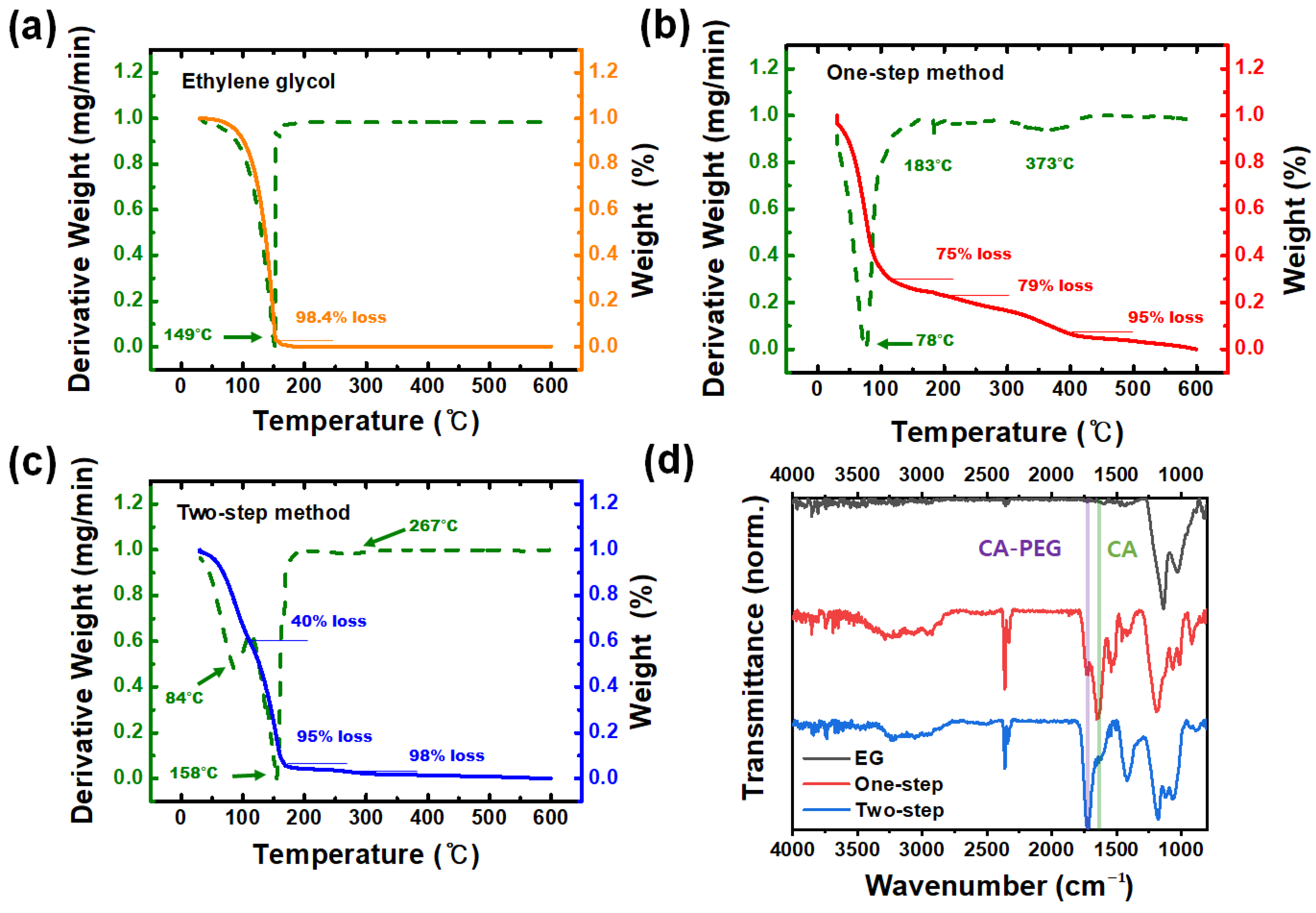
Figure 2a–c show the TGA curves of the EG, the one-step-coated film, and the two-step-coated film. The weight loss at ~80 °C is attributed to the elimination of the remaining or absorbed water molecules. Secondly, the weight loss at around 150 °C corresponds to the decomposition of EG and sulfate ions, which is followed by the continuous decomposition of citric acid complexes. The elevated EG decomposition temperature in the mixture film implies that the polyesterification takes place for both cases.
The FT-IR spectra of the EG, one-step-coated film, and two-step-coated film before sintering are presented in Figure 2d. Characteristic peaks for the ester bond between CA and EG appears at 1717–1733 cm−1, while the peak located at 1645 cm−1 corresponds to residual CA. In the case of films coated with the two-step method, compared to the one-step method, the former pick is more prominent than the latter, meaning that polyesterification occurs more vigorously and there is less residual CA after spin coating.
Figure 3a–d show SEM images of BeO layer surfaces created by the two-step spin-coating method depending on the content ratio (0.5:1, 1:1, 2:1, and 3:1) of CA to BeSO4 after sintering at 1500 °C for three hours. Although our modified Pechini method includes polyesterification on the substrate, the ratio of the precursor solutions must be carefully organized to ensure a fine sol–gel film because the Be cations are allowed to disperse and infiltrate throughout the citric acid in water, similar to the conventional Pechini method. As a result, the surfaces of the sintered BeO film are found to be relatively regular in each set of Be citrate solution conditions. The high concentration of Be cations in the 0.5:1 CA/BeSO4 solution produced the grainy surface as shown in Figure 3a. At a ratio of 1:1, however, a smoother surface is observed with a morphology indicative of high-quality thin film growth. The surface morphology is improved at a CA to BeSO4 ratio of 1:1 compared to the other surfaces because metal ions are well dispersed and the nucleation and growth process is optimized. Remarkably, the 1:1 molar ratio of CA and metal salt used in conventional Pechini powder synthesis is also effective with the proposed process [15,20].
When the ratio of CA to BeSO4 reaches 2:1 and 3:1, microstructural growth on the surface appears to progress by phase irregularities depending on the EG and CA concentrations. The distribution of the coalesced region is reduced when decreasing the content of BeSO4 relative to the content of CA. At CA/BeSO4 ratios of 2:1 and 3:1, lower coverage of the BeO thin films on the surface arise due to the phase separation of the sol–gel film due to the fewer metal cations that exist after varying the stoichiometric balance of the monomers (EG) in the mixture [21]. Overall, the correlation among the amount of Be ions in the Be citrate solution, the grain size, and the degree of coalescence are revealed by the surface morphology of the BeO thin film [22,23].
Figure 4a–c show SEM images of the change in the morphology of the BeO with a CA/BeSO4 ratio of 1:1 depending on sintering temperatures of 1100 °C, 1300 °C, and 1500 °C. According to the structural change in the surface, the serial process of the formation of the thin film can be indirectly inferred. Although thin film growth in our case begins with a precursor film and becomes a thin film, the route of the thin film formation process of “nucleation-nuclei growth-coalescence-continuous film” can be correspondingly observed [24,25,26]. After nucleation and nuclei growth (the initial stage of the Pechini method), the island microstructure aggregates into sub-micron particles of BeO, which were observed to gather in an irregular structure according to the image taken at 1100 °C at a higher resolution. At the sintering temperature of 1300 °C, the island microstructures are more condensed and ordered compared with those at 1100 °C. The hexagonal-like grains of the BeO layer were locally grown and covered the surface of the space between the island microstructures (Figure S3) caused by the effect of the increased lateral atomic diffusion due to the higher sintering temperature. When the sintering temperature reaches 1500 °C, the island layer is filled, and a continuous BeO thin film is completed. Additionally, the grain size is significantly larger, and smaller grains exist between the larger grains. A cross-sectional SEM image of the BeO layer is shown in Figure S3, but the thickness of the BeO layer is not distinguishable in this case because the conductivity of both the BeO layer and the sapphire substrate were insufficient.
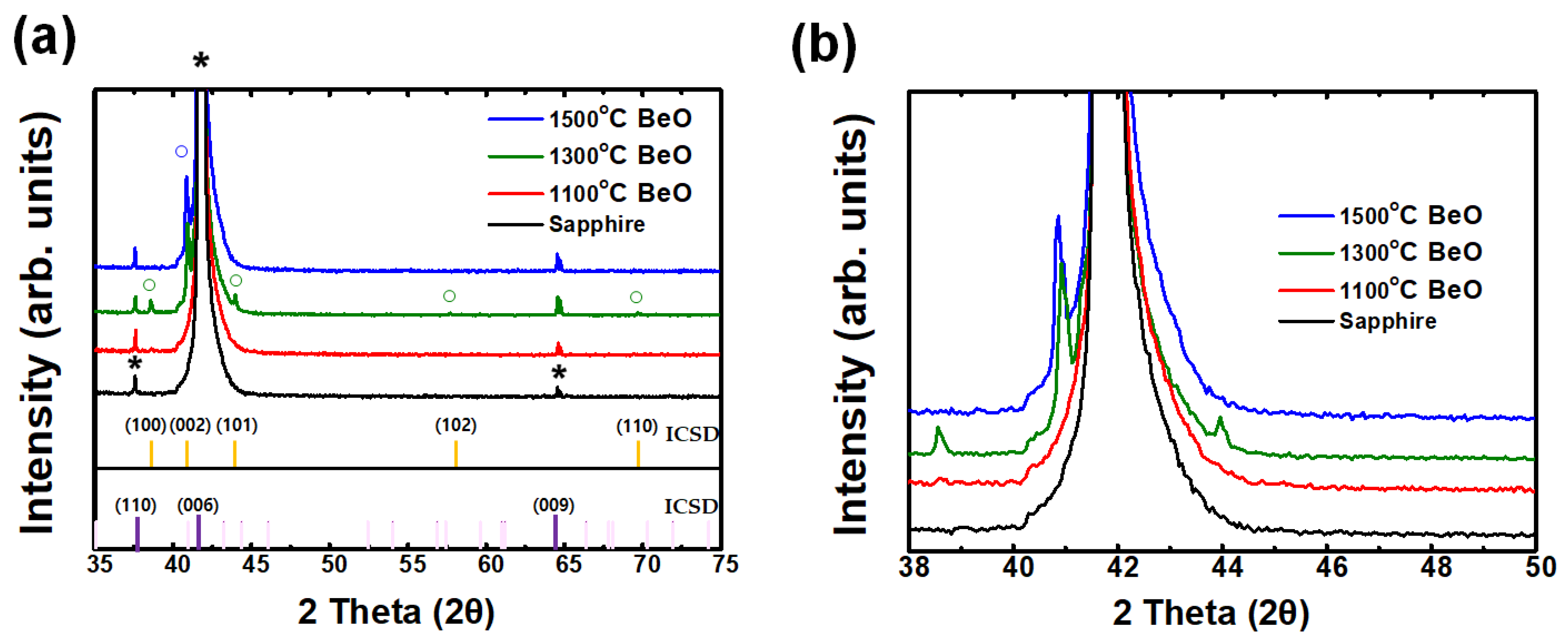
Figure 5a,b show the XRD characterization results of a BeO thin film on a sapphire substrate according to the sintering temperature. The XRD patterns of BeO were marked at 38.65°, 41.32°, 44.05°, 57.86°, and 69.94°, corresponding to the (100), (002), (101), (102), and (110) planes according to the inorganic crystal structure database (ICSD) [10]. Except for the XRD peaks corresponding to sapphire (ICSD), the XRD peaks of the BeO thin film differed according to the sintering temperature, indicating a change in the crystallinity of the BeO thin films. The island microstructure in BeO under the 1100 °C sintering condition, as discussed in the SEM section, was considered an amorphous structure because the significant signal for the crystal structure corresponding to BeO did not appear in the XRD data. In the XRD peaks of the BeO thin films at a higher sintering temperature, however, the crystallinity of BeO became apparent. The XRD peaks of the BeO thin film at the sintering temperature of 1300 °C were detected at 38.55°, 40.91°, 43.96°, 57.72° (circled in the graph), and 69.70° (circled in the graph), indicative of the BeO powder crystal structure. In this case, the peak of 40.91° was remarkably enhanced, corresponding to the (002) plane. Particularly, a single XRD peak at 40.86° was observed for the BeO thin film sintered at 1500 °C, and the XRD pattern related to the BeO bulk structure disappeared. An increase in the XRD peak intensity at 40.86 was also observed in recent research focusing on BeO (002) grown on Si (002) by atomic layer deposition [27]. This result signifies that the BeO structure on the sapphire gained the preferred orientation by annealing. The single peak in the BeO thin film sintered at 1500 °C showed a slight shift at 0.05° from that of BeO sintered at 1300 °C, providing evidence of the widened lattice distance on the (002) plane and implying tensile strain of the BeO thin film [27,28]. Hence, the XRD analysis indicated the formation process of the BeO thin film specimen, particularly the crystal structure, with the results being in good agreement with the SEM images.
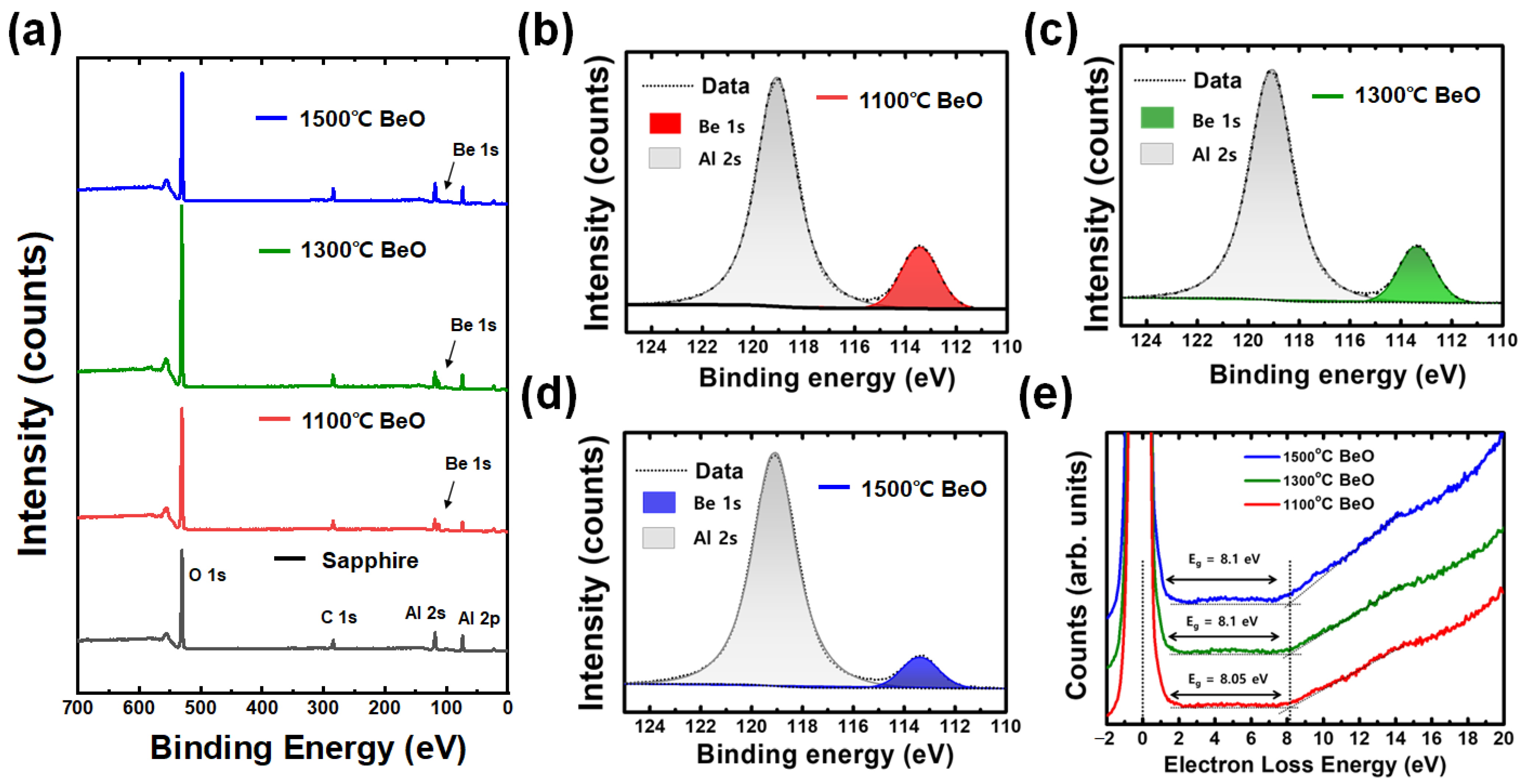
Figure 6a shows the XPS data of the BeO thin film specimens according to the sintering temperature, as used to analyze the elemental/chemical state change of BeO thin films. The wide survey scan shows the Al 2p, C 1 s, and O 1 s peaks at binding energies of 73.62 eV, 284.62 eV, and 530.62 eV, respectively [29,30,31]. The Be 1 s and Al 2 s peaks were convoluted due to the overlapping of the Be 1 s and Al 2 s orbital energy levels; these are separately plotted as the high-resolution spectra in each case depending on the sintering temperature and are fitted as shown in Figure 5. The complete Be oxidation by the sintering process enhanced the portion of the Be-O-dominant spectra at 113.5 eV, while the chemical states of the Be-Be bonds when the binding energy was 110.7 eV were absent [29]. Furthermore, the Al-O peak at 119.0 eV represents the photoelectrons of Al 2 s in the sapphire substrate due to the penetration of X-rays into the BeO thin films [30,32]. Figure 6e shows the REELS fitting of the optical bandgap of BeO thin films with different sintering temperatures. The optical bandgaps of BeO layers after sintering at 1100 °C, 1300 °C, and 1500 °C were 8.05 eV, 8.1 eV, and 8.1 eV, respectively. Earlier related studies reported similar values of 8.0 eV, 8.57 eV (theoretically), and 10.7 eV (experimentally) [33,34,35]. Unfortunately, the bandgap differences in BeO layers after sintering at 1100 °C, 1300 °C, and 1500 °C were insufficient due to the X-ray penetration onto the BeO layer, but the bandgap values of the BeO layers at higher sintering temperatures were slightly larger than those at a lower sintering temperature.
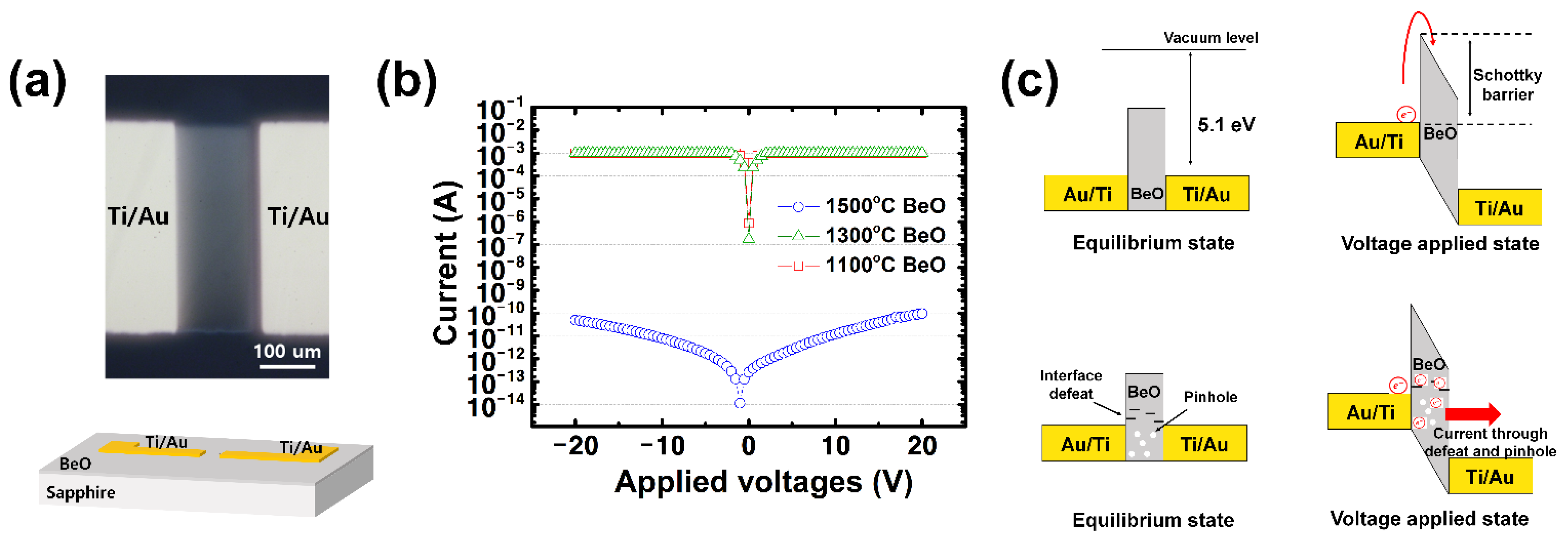
The OM image of the MIM device under the 1500 °C sintering condition and the I-V characteristics of the MIM device with BeO thin films created with different sintering temperatures are correspondingly shown in Figure 7a,b. In the OM image, the patterned active channel distances between the lateral electrodes are 150 μm, and the width is 385 μm. Although the active channel was patterned with a shadow mask for the lateral structure of the MIM device, an additional process such as wet etching is also possible if the proper etchants are used [36]. Contrary to the smooth surface of the active region, numerous defects and pinholes can be observed in the OM images of the active region of the MIM device with BeO layers after sintering at 1100 °C and 1300 °C (Supplementary Figure S4). The pinholes and defects formed on the surface or inside of the Insulating layer are directly related to the significant deterioration of the insulating capabilities of the insulating layer [37,38,39].
The currents of the MIM device with the BeO thin film specimens sintered at 1100 °C and 1300 °C showed considerable increases and reached compliance current levels at applied voltages of 2.0 V and 1.9 V, respectively, indicating electron-transportable sites in the active layer. The breakdown voltages of the MIM devices were not clearly observed because the leakage current levels of those were rapidly increased at low applied voltages. However, the current of the MIM device with the BeO thin film sintered at 1500 °C gradually increased below the nA range due to the applied voltages under both positive and negative bias. The leakage currents were 49 pA and 95 pA at −20 V and + 20 V, respectively, while no breakdown voltage arose in the MIM device with the BeO thin film sintered at 1500 °C over the voltage sweeping range of −20 V to 20 V, indicating that the BeO thin film is an excellent gate oxide candidate. Figure 7c shows a schematic diagram and an illustration of the leakage current flowing into the insulator layer due to the defects and pinholes between the electrodes and the insulating layer. Consequently, the firm Schottky barrier between the insulator and the metal with fewer defects and pinholes contributes to ensuring the low leakage current of the insulating layer when using a BeO layer created at a higher sintering temperature [40,41].

4. Conclusions

In conclusion, we introduced a novel modified Pechini synthesis approach for the formation of BeO thin films based on a sequential spin-coating method used to apply MIM devices as an insulator layer. We also focused on optimizing the surface morphologies of the BeO thin film depending on the polyesterification condition and the sintering temperature. The morphologies and the crystal structures of the BeO thin film changed dramatically from an amorphous microstructure to a continuous thin film according to the sintering temperature. The bandgap of the BeO thin film was measured at 8.1 eV by REELS fitting. Lateral structured MIM devices were manufactured to assess the insulation capabilities of the BeO thin film specimens. The leakage current was found to be below the 49 pA and 95 pA ranges from −20 V to 20 V for the BeO thin film created by our modified Pechini method at a sintering temperature of 1500 °C. These results help further the understanding of the morphology and the leakage current features of BeO thin films used as metal oxides, insulators, and dielectric layers for future applications.

5. Patents

This section is not mandatory but may be added if there are patents resulting from the work reported in this manuscript.

Supplementary Materials

The following are available online at https://www.mdpi.com/article/10.3390/electronics12010047/s1, Figure S1: Images of the precursor and BeO layer manufactured by the conventional Pechini thin film method. The form factor of the final film was powder due to the high viscosity of the precursor solution before and as deposited onto the substrate, Figure S2: SEM images and EDS analysis outcome of the BeO thin film after sintering at a temperature of 1300 °C as mentioned in relation to the distribution of Be, O, Al atoms in the green square area in the image. According to the EDS analysis and the distribution of Be atoms, the areas between the island structures were covered by the BeO thin film, Figure S3. The cross-sectional image of the BeO layer fabricated by two-step spin-coated before the BeO layer was sintered by 1500 °C. Figure S4: Optical microscope images of the distances of the both metals and the surface morphologies of the metal–insulator–metal device sintered at (a) 1500 °C, (b) 1300 °C, and (c) 1100 °C.

Author Contributions

Y.P.J.: Writing—original draft, conceptualization, writing—review and editing, data curation, formal analysis, investigation, methodology, software, and visualization. D.H.: Writing—original draft, writing—review and editing, conceptualization, and formal analysis. S.-h.L.: formal analysis, methodology, and writing—review and editing. E.J.L.: data curation, software, and visualization. T.W.C.: data curation and formal analysis. D.Y.K.: data curation and investigation. C.Y.K.: data curation and investigation. J.P.: supervision, methodology, and writing—review and editing. Y.J.K.: supervision, methodology, and writing—review and editing. Y.J.Y.: supervision, funding acquisition, resources, methodology, validation, writing—review and editing, and conceptualization. S.Y.P.: supervision, funding acquisition, resources, methodology, project administration, validation, writing—review and editing, and conceptualization. All authors have read and agreed to the published version of the manuscript.

Funding

This research was supported by the Nano-Material Technology Development Program through the National Research Foundation of Korea (NRF) funded by the Ministry of Science and ICT (No. 2018M3A7B4070990). Additional support came from a grant from the National Research Foundation of Korea (NRF) funded by the Korean Government (MSIT) (Nos. 2020R1A2C2103137, 2020R1F1A1076359, and 2022R1C1C2011696) and from the Materials, Components and Equipment Research Program funded by Gyeonggi Province (No. AICT-018-T3).

Data Availability Statement

The data that support the findings of this study are available from the corresponding author upon reasonable request.

Conflicts of Interest

The authors declare no conflict of interest.

References

  1. Zhang, H.; Holbrook, M.; Cheng, F.; Nam, H.; Liu, M.; Pan, C.-R.; West, D.; Zhang, S.; Chou, M.Y.; Shih, C.-K. Epitaxial growth of two-dimensional insulator monolayer honeycomb BeO. ACS Nano 2021, 15, 2497–2505. [Google Scholar] [CrossRef] [PubMed]
  2. Gaskins, J.T.; Hopkins, P.E.; Merrill, D.R.; Bauers, S.R.; Hadland, E.; Johnson, D.C.; Koh, D.; Yum, J.H.; Banerjee, S.; Nordell, B.J.; et al. Investigation and review of the thermal, mechanical, electrical, optical, and structural properties of atomic layer deposited high-k dielectrics: Beryllium oxide, aluminum oxide, hafnium oxide, and aluminum nitride. ECS J. Solid State Sci. Technol. 2017, 6, N189. [Google Scholar] [CrossRef] [Green Version]
  3. Li, W.; Mingo, N. Thermal conductivity of bulk and nanowire InAs, AlN, and BeO polymorphs from first principles. J. Appl. Phys. 2013, 114, 183505. [Google Scholar] [CrossRef]
  4. Mortazavi, B.; Shojaei, F.; Rabczuk, T.; Zhuang, X. High tensile strength and thermal conductivity in BeO monolayer: A first-principles study. FlatChem 2021, 28, 100257. [Google Scholar] [CrossRef]
  5. Slack, G.A.; Austerman, S.B. Thermal conductivity of BeO single crystals. J. Appl. Phys. 1971, 42, 4713–4717. [Google Scholar] [CrossRef]
  6. Malakkal, L.; Szpunar, B.; Siripurapu, R.K.; Zuniga, J.C.; Szpunar, J.A. Thermal conductivity of wurtzite and zinc blende cubic phases of BeO from ab initio calculations. Solid State Sci. 2017, 65, 79–87. [Google Scholar] [CrossRef]
  7. Yim, K.H.; Yong, Y.; Lee, J.H.; Lee, K.H.; Nahm, H.-H.; Yoo, J.H.; Lee, C.H.; Hwang, C.S.; Han, S.W. Novel high-κ dielectrics for next-generation electronic devices screened by automated ab initio calculations. NPG Asia Mater. 2015, 7, e190. [Google Scholar] [CrossRef]
  8. Roessler, D.M.; Walker, W.C.; Loh, E. Electronic spectrum of crystalline beryllium oxide. J. Phys. Chem. Solids 1969, 30, 157–167. [Google Scholar] [CrossRef]
  9. Hazen, R.M.; Finger, L.W. High-pressure and high-temperature crystal chemistry of beryllium oxide. J. Appl. Phys. 1986, 59, 3728–3733. [Google Scholar] [CrossRef]
  10. Schirmer, O.F. The structure of the paramagnetic lithium center in zinc oxide and beryllium oxide. J. Phys. Chem. Solids 1968, 29, 1407–1429. [Google Scholar] [CrossRef]
  11. Smith, D.K.; NewKirk, H.W.; Kahn, J.S. The crystal structure and polarity of beryllium oxide. J. Electrochem. Soc. 1964, 111, 78. [Google Scholar] [CrossRef]
  12. Felten, E.J. Sintering behavior of beryllium oxide. J. Am. Ceram. Soc. 1961, 44, 251–255. [Google Scholar] [CrossRef]
  13. Emsley, J. Nature’s building blocks: An A-Z guide to the elements; Oxford University Press: Oxford, UK, 2003; p. 57. [Google Scholar]
  14. Luckey, T.D.; Venugopal, B. Physiologic and Chemical Basis for Metal Toxicity; Springer: Berlin/Heidelberg, Germany, 1977; pp. 167–168. [Google Scholar]
  15. Pechini, M.P. Method of Preparing Lead and Alkaline Earth Titanates and Niobates and Coating Method Using the Same to form a Capacitor. U.S. Patent US3330697A, 11 July 1967. [Google Scholar]
  16. Wang, X.; Wang, R.; Peng, C.; Li, T.; Liu, B. Polyacrylamide gel method: Synthesis and property of BeO nanopowders. J. Sol-Gel Sci. Technol. 2011, 57, 115–127. [Google Scholar] [CrossRef]
  17. Dimesso, L. Pechini Processes: An Alternate Approach of the Sol–Gel Method, Preparation, Properties, and Applications. In Handbook of Sol-Gel Science and Technology; Springer: Cham, Switzerland, 2016. [Google Scholar] [CrossRef]
  18. Lu, X.; Wang, T.; Zhang, Y.; Shahzad, M.B.; Qi, Y. An enhancement in structural and superconducting properties of Bi2212 epitaxial thin films grown by the Pechini sol–gel method. J. Appl. Crystallogr. 2013, 46, 379–386. [Google Scholar] [CrossRef]
  19. Im, J.-H.; Kim, H.-S.; Park, N.-G. Morphology-photovoltaic property correlation in perovskite solar cells: One-step versus two-step deposition of CH3NH3PbI3. APL Mater. 2014, 2, 081510. [Google Scholar] [CrossRef] [Green Version]
  20. Mohassel, R.; Sobhani, A.; Salavati-Niasari, M.; Goudarzi, M. Pechini synthesis and characteristics of Gd2CoMnO6 nanostructures and its structural, optical and photocatalytic properties. Spectrochim. Acta Part A Mol. Biomol. Spectrosc. 2018, 204, 232–240. [Google Scholar] [CrossRef]
  21. Rudisill, S.G.; Hein, N.M.; Terzic, D.; Stein, A. Controlling microstructural evolution in pechini gels through the interplay between precursor complexation, step-growth polymerization, and template confinement. Chem. Mater. 2013, 25, 745–753. [Google Scholar] [CrossRef]
  22. Sarakinos, K. A review on morphological evolution of thin metal films on weakly-interacting substrates. Thin Solid Film. 2019, 688, 137312. [Google Scholar] [CrossRef]
  23. Teixeira, M.S.M.; Santos, L.M.N.B.F.; Costa, J.C.S. Nucleation, coalescence, and thin-film growth of triflate-based ionic liquids on ITO, Ag, and Au surfaces. Coll. Interfaces 2022, 6, 46. [Google Scholar] [CrossRef]
  24. Legg, B.A.; Voïtchovsky, K.; De Yireo, J.J. Hydroxide films on mica form charge-stabilized microphases that circumvent nucleation barriers. Sci. Adv. 2022, 8, eabn7087. [Google Scholar] [CrossRef]
  25. Guo, X.; Tan, Y.; Hu, Y.; Zafar, Z.; Liu, J.; Zou, J. High quality VO2 thin films synthesized from V2O5 powder for sensitive near-infrared detection. Sci. Rep. 2021, 11, 21749. [Google Scholar] [CrossRef] [PubMed]
  26. LaFollette, D.K.; Canova, K.L.; Zhang, Z.V.; Abelson, J.R. Coalescence of ultrathin films by atomic layer deposition or chemical vapor deposition: Models of the minimum thickness based on nucleation and growth rates. J. Vac. Sci. Technol. A Vac. Surf. Film. 2022, 40, 023403. [Google Scholar] [CrossRef]
  27. Jang, Y.S.; Jung, D.H.; Sultane, P.R.; Larsen, E.S.; Bielawski, C.W.; Oh, J.W. Low temperature growth of beryllium oxide thin films prepared via plasma enhanced atomic layer deposition. Appl. Surf. Sci. 2022, 572, 151405. [Google Scholar] [CrossRef]
  28. Kim, H.-S.; Park, N.-G. Importance of tailoring lattice strain in halide perovskite crystals. NPG Asia Mater. 2020, 12, 78. [Google Scholar] [CrossRef]
  29. Mallinson, C.F.; Castle, J.E. Beryllium and beryllium oxide by XPS. Surf. Sci. Spectra 2013, 20, 86–96. [Google Scholar] [CrossRef] [PubMed] [Green Version]
  30. Prakash, R.; Kumar, S.; Kumar, V.; Choudhary, R.J.; Phase, D.M. Optical and x-ray photoelectron spectroscopy studies of α-Al2O3. AIP Conf. Proc. 2016, 1731, 050097. [Google Scholar]
  31. Tago, T.; Kataoka, N.; Tanaka, H.; Kinoshita, K.; Kishida, S. XPS study from a clean surface of Al2O3 single crystals. Procedia Eng. 2017, 216, 175–181. [Google Scholar] [CrossRef]
  32. Jung, D.H.; Jang, Y.S.; Sultane, P.R.; Bielawski, C.W.; Oh, J.W. Energy band offsets of BeO dielectrics grown via atomic-layer deposition on β-Ga2O3 substrates. J. Alloy. Compd. 2022, 922, 166197. [Google Scholar] [CrossRef]
  33. Yum, J.H.; Bersuker, G.; Ferrer, D.A.; Akyol, T.; Lei, M.; Park, K.W.; Hudnall, T.W.; Downer, M.C.; Bielawski, C.W.; Yu, E.T.; et al. ALD beryllium oxide: Novel barrier layer for high performance gate stacks on Si and high mobility substrates. In Proceedings of the 2011 International Electron Devices Meeting, Washington, DC, USA, 5–7 December 2011; IEEE: New York, NY, USA, 2011. [Google Scholar]
  34. Koh, D.; Banerjee, S.K.; Brockman, J.; Kuhn, M.; King, S.W. X-ray photoelectron spectroscopy investigation of the valence band offset at beryllium oxide-diamond interfaces. Diam. Relat. Mater. 2020, 101, 107647. [Google Scholar] [CrossRef]
  35. Valedbagi, S.; Jalilian, J.; Elahi, S.M.; Majidi, S.; Fathalian, A.; Dalouji, V. Ab initio calculations of electronic and optical properties of BeO nanosheet. Electron. Mater. Lett. 2014, 10, 5–11. [Google Scholar] [CrossRef]
  36. Austerman, S.B.; Newkirk, J.B.; Smith, D.K.; Newkirk, H.W. Etching studies of beryllium oxide crystals. J. Mater. Sci. 1967, 2, 378–387. [Google Scholar] [CrossRef]
  37. Chia, C.; Schulaker, M.M.; Provine, J.; Jeffrey, S.S.; Howe, R.T. ALD HfO2 films for defining microelectrodes for electrochemical sensing and other applications. ACS Appl. Mater. Interfaces 2019, 11, 26082–26092. [Google Scholar] [CrossRef] [PubMed]
  38. Dongquoc, V.; Seo, D.-B.; Anh, C.V.; Lee, J.-H.; Park, J.-H.; Kim, E.-T. Controlled surface morphology and electrical properties of sputtered titanium nitride thin film for metal–insulator–metal structures. Appl. Sci. 2022, 12, 10415. [Google Scholar] [CrossRef]
  39. Sun, S.; Lawandi, S.R.; Sarangan, A.M.; Banerjee, P.P. Dark electron tunneling current in metal–insulator–metal structures: Modeling, fabrication, and measurement. Opt. Eng. 2022, 61, 027101. [Google Scholar] [CrossRef]
  40. Qaid, M.M.; AlSalhi, M.S. Leakage current and charge transport mechanism in Poly(phenylene oxdie)-conductor Schottly bilayers. Mater. Chem. Phys. 2021, 259, 124054. [Google Scholar] [CrossRef]
  41. Ma, J.; Matioli, E. 2 kV slanted tri-gate GaN-on-Si Schottky barrier diodes with ultra-low leakage current. Appl. Phys. Lett. 2018, 112, 052101. [Google Scholar] [CrossRef]
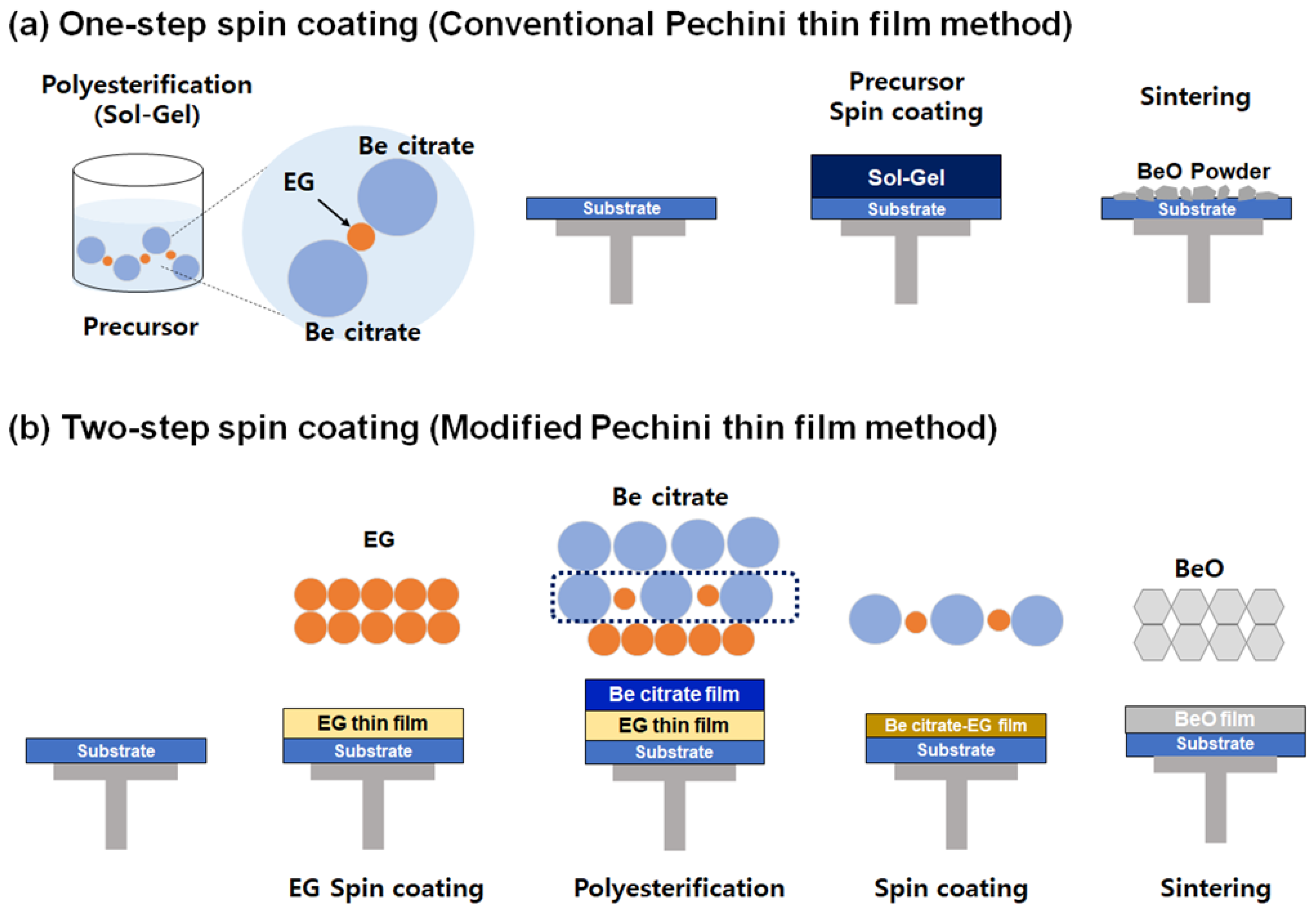
Figure 1. Illustrations of the (a) one-step and (b) two-step spin-coating deposition processes used to create the BeO thin film specimens along with a schematic diagram of the formation progress of the BeO thin film.
Electronics 12 00047 g001
Figure 2. Thermogravimetric analyzer (TGA) data for the solutions of (a) ethylene glycol and (b) the one-step and (c) two-step spin-coating precursors to form the BeO layers; (d) Fourier transform infrared (FTIR) analysis outcomes for each of the solutions.
Electronics 12 00047 g002
Figure 3. Scanning electron microscope images of the surfaces for the beryllium oxide layers created by the two-step spin-coating method depending on the content ratio: (a) 0.5:1, (b) 1:1, (c) 2:1, and (d) 3:1 citric acid and beryllium sulfate.
Electronics 12 00047 g003
Figure 4. Scanning electron microscope (SEM) images of the surfaces of the BeO thin films with a 1:1 ratio of CA/BeSO4 created by the two-step spin-coating method following sintering at temperatures of (a) 1100 °C, (b) 1300 °C, and (c) 1500 °C.
Electronics 12 00047 g004
Figure 5. X-ray diffraction (XRD) peaks at a CA/BeSO4 ratio of 1:1 of BeO thin films depending on the sintering temperature. The XRD peaks corresponding to BeO and sapphire are correspondingly denoted with the circle and star symbols and the crystal planes presented in yellow and purple. The bar graphs in yellow and purple are citied the XRD peaks of BeO and sapphire by the inorganic crystal structure database (ICSD) respectively.
Electronics 12 00047 g005
Figure 6. (a) X-ray photoelectron spectroscopy (XPS) of the BeO thin films on sapphire substrates as a function of the binding energy from 0 eV to 850 eV and the high-resolution spectrum with fitting results corresponding to Be 1 s (Be-O) and Al 2 s depending on the sintering temperatures of (b) 1100 °C, (c) 1300 °C, and (d) 1500 °C. (e) The reflection electron energy loss spectroscopy (REELS) of the BeO thin film is shown.
Electronics 12 00047 g006
Figure 7. Insulating performance of beryllium oxide (BeO) thin films created by the two-step method: (a) the device structure is a metal–insulator–metal (MIM) device sandwiched in the form of Au/Ti/BeO thin film/Ti/Au. (b) The current–voltage bias under sweep mode is indicative of the leakage current over the applied voltage range of −20 V to 20 V with a compliance current of 1 mA and is plotted here on log scale on the current axis. (c) A schematic illustration of the leakage current passing through the MIM device, exiting through the interfacial defects and pinholes in the BeO layers.
Electronics 12 00047 g007
Disclaimer/Publisher’s Note: The statements, opinions and data contained in all publications are solely those of the individual 165 author(s) and contributor(s) and not of MDPI and/or the editor(s). MDPI and/or the editor(s) disclaim responsibility for any injury to 166 people or property resulting from any ideas, methods, instructions or products referred to in the content.