
Graphene and Two-Dimensional Materials-Based Flexible Electronics for Wearable Biomedical Sensors

 , , and
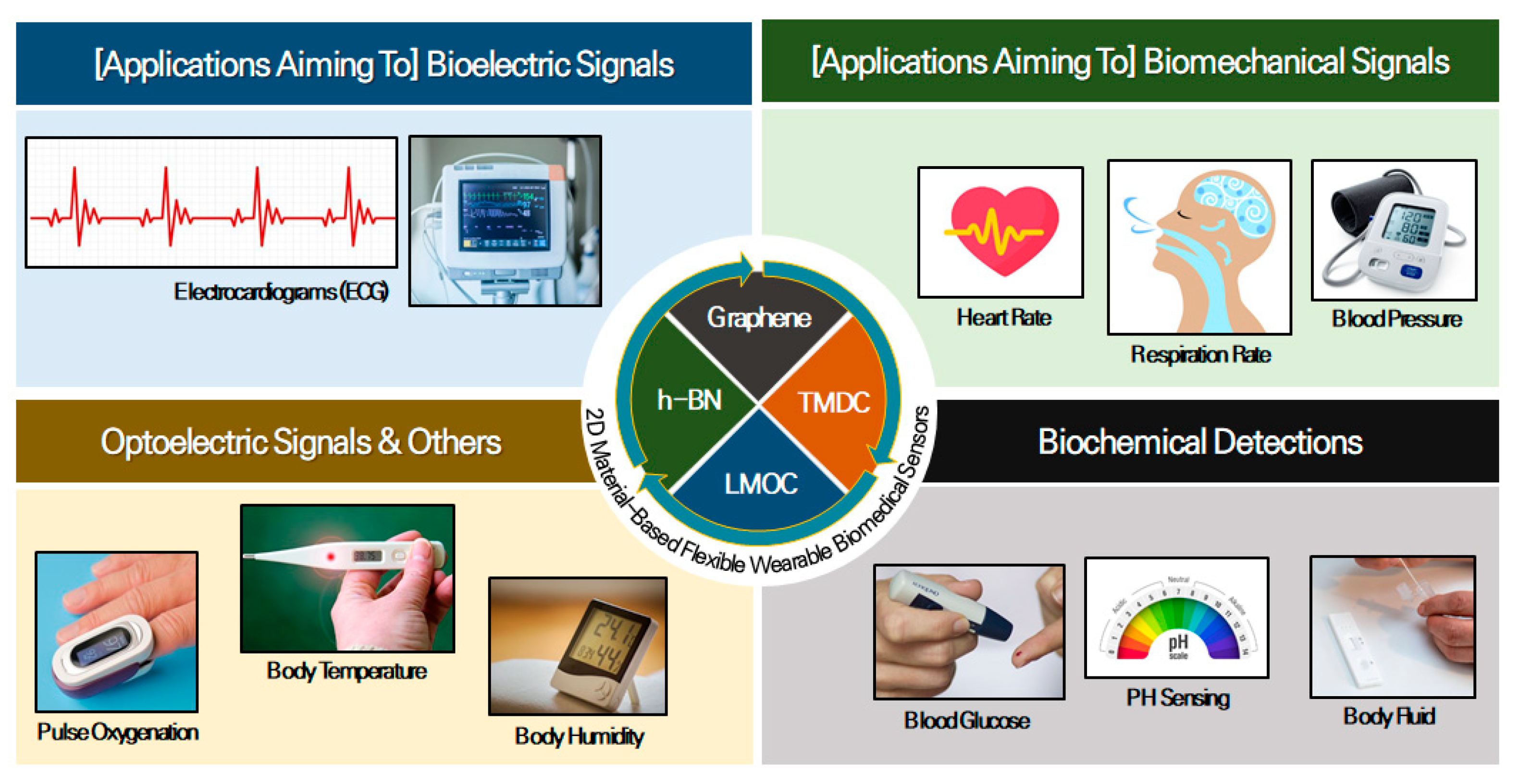
Abstract
1. Introduction
2. Two-Dimensional Materials with Electrical and Optical Properties
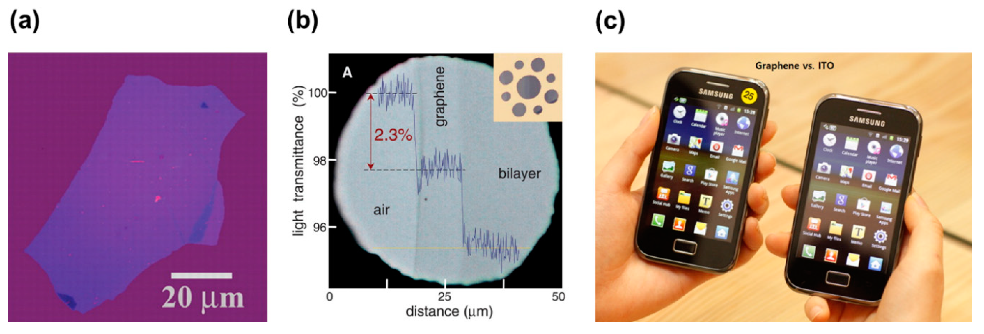
2.1. Graphene

2.2. MoS2 (a 2D Transition Metal Dichalcogenide Material)

2.3. 2D Layered Metal Oxychalcogenide Materials
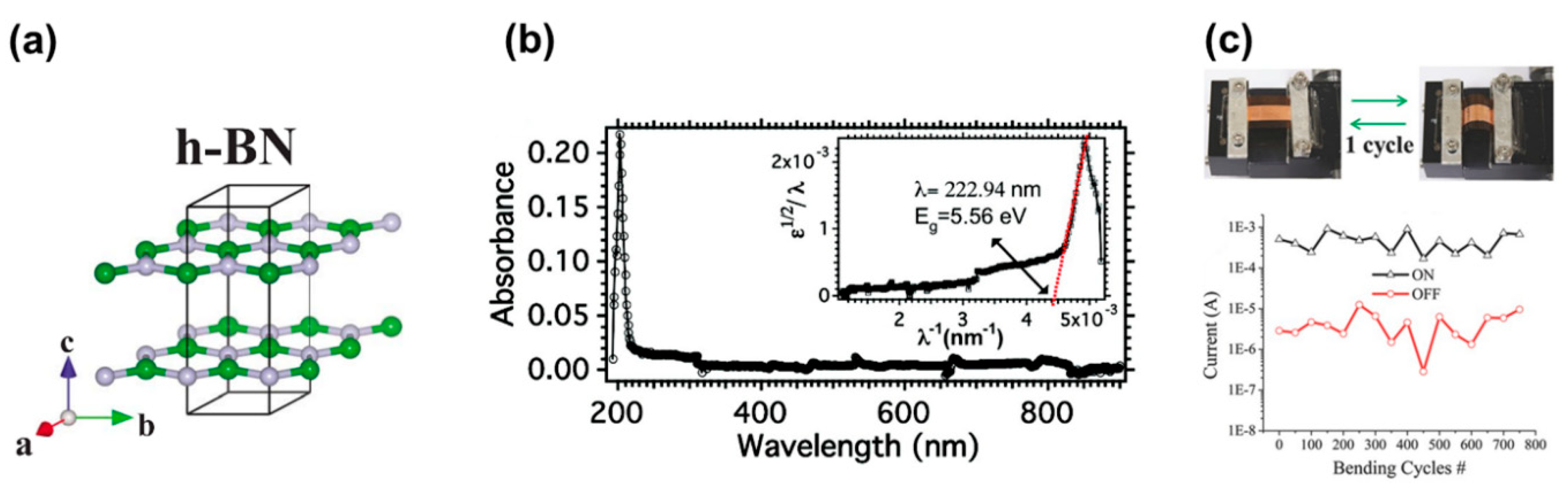
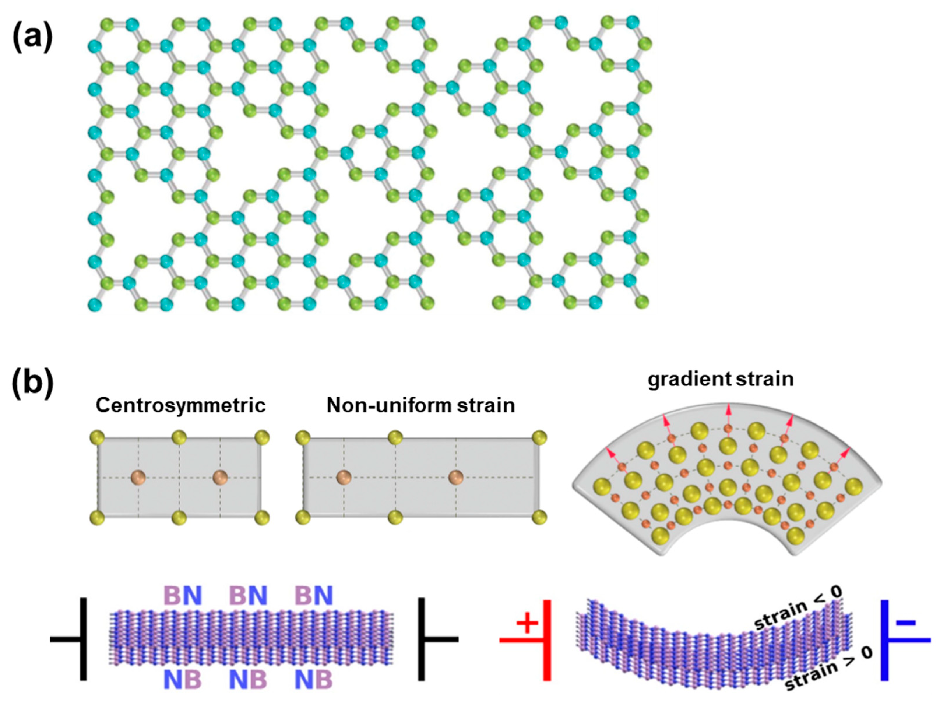
2.4. Hexagonal Boron Nitride (2D Insulator)

3. Two-Dimensional Materials with Piezoelectric and Flexoelectric Properties
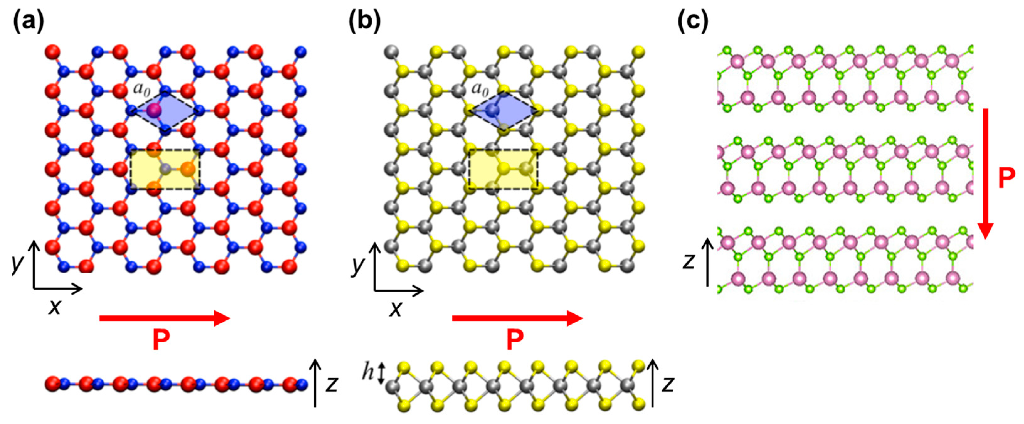
3.1. Non-Centrosymmetric 2D Piezoelectric Materials


3.2. 2D Piezoelectric Materials through Surface Engineering
3.3. 2D Flexoelectric Materials
4. Two-Dimensional Materials-Based Wearable Biomedical Sensors
4.1. Wearable Biomedical Sensors for Physical Detection
4.1.1. Bioelectrical Signals


4.1.2. Biomechanical Signals
4.1.3. Optoelectric Signals
4.1.4. Body Temperature
4.2. Wearable Biomedical Sensors for Chemical Detection
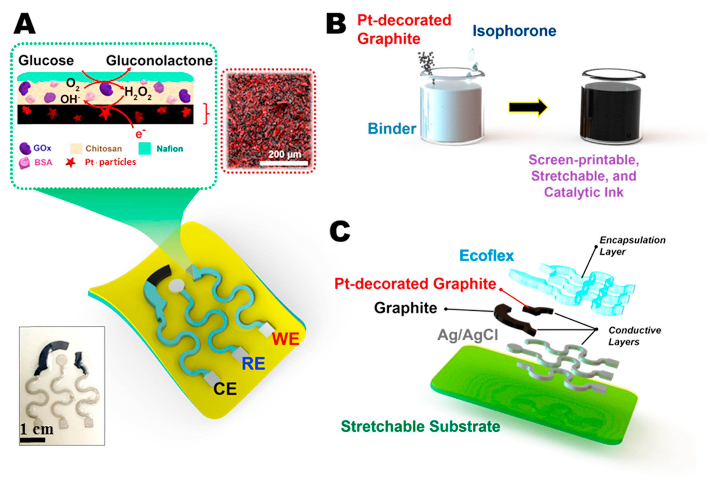
4.2.1. Glucose
4.2.2. pH Sensing
5. Conclusions
Author Contributions
Funding
Acknowledgments
Conflicts of Interest
References
- Geim, A.K.; Novoselov, K.S. The rise of graphene. Nature Mater. 2007, 6, 183–191. [Google Scholar] [CrossRef] [PubMed]
- Wang, W.; Su, H.; Wu, Y.; Zhou, T.; Li, T. Review—Biosensing and Biomedical Applications of Graphene: A Review of Current Progress and Future Prospect. J. Electrochem. Soc. 2019, 166, B505. [Google Scholar] [CrossRef]
- Cao, X.; Halder, A.; Tang, Y.; Hou, C.; Wang, H.; Øllgaard Duus, J.; Chi, Q. Engineering two-dimensional layered nanomaterials for wearable biomedical sensors and power devices. Mater. Chem. Front. 2018, 2, 1944–1986. [Google Scholar] [CrossRef]
- Pang, Y.; Yang, Z.; Yang, Y.; Ren, T.-L. Wearable Electronics Based on 2D Materials for Human Physiological Information Detection. Small 2020, 16, 1901124. [Google Scholar] [CrossRef] [PubMed]
- Minu, M.; Sithara, R.; Antara, V.; Brahmananda, C.; Chandra Sekhar, R. Flexible and wearable electrochemical biosensors based on two-dimensional materials: Recent developments. Anal. Bioanal. Chem. 2021, 413, 727–762. [Google Scholar]
- Han, D.-W.; Hong, S.W. Multifaceted Biomedical Applications of Graphene; Springer: Berlin, Germany, 2022; ISBN 978-981-16-4923-3. [Google Scholar]
- Nurunnabi, M.; McCarthy, J. Biomedical Applications of Graphene and 2D Nanomaterials; Elsevier: Amsterdam, The Netherlands, 2019; ISBN 9780128162699. [Google Scholar]
- Biomedical Advances through Use of Graphene. Available online: https://cordis.europa.eu/article/id/243655-biomedical-advances-through-use-of-graphene (accessed on 8 December 2022).
- Novoselov, K.S.; Geim, A.K.; Morozov, S.V.; Jiang, D.; Zhang, Y.; Dubonos, S.V.; Grigorieva, I.V.; Firsov, A.A. Electric field effect in atomically thin carbon films. Science 2004, 306, 666–669. [Google Scholar] [CrossRef] [PubMed]
- Nair, R.R.; Blake, P.; Grigorenko, A.N.; Novoselov, K.S.; Booth, T.J.; Stauber, T.; Peres, N.M.R.; Geim, A.K. Fine structure constant defines visual transparency of graphene. Science 2008, 320, 1308. [Google Scholar] [CrossRef]
- Lee, C.; Wei, X.; Kysar, J.W.; Hone, J. Measurement of the elastic properties and intrinsic strength of monolayer graphene. Science 2008, 321, 385–388. [Google Scholar] [CrossRef]
- Kim, K.S.; Zhao, Y.; Jang, H.; Lee, S.Y.; Kim, J.M.; Kim, K.S.; Ahn, J.-H.; Kim, P.; Choi, J.-Y.; Hong, B.H. Large-scale pattern growth of graphene films for stretchable transparent electrodes. Nature 2009, 457, 706–710. [Google Scholar] [CrossRef]
- Akinwande, D.; Brennan, C.J.; Bunch, J.S.; Egberts, P.; Felts, J.R.; Gao, H.; Huang, R.; Kim, J.-S.; Li, T.; Li, Y.; et al. A review on mechanics and mechanical properties of 2D materials—Graphene and beyond. Extreme Mech. Lett. 2017, 13, 42–77. [Google Scholar] [CrossRef]
- Allen, M.J.; Tung, V.C.; Kaner, R.B. Honeycomb carbon: A review of graphene. Chem. Rev. 2010, 110, 132–145. [Google Scholar] [CrossRef] [PubMed]
- Kim, S.J.; Choi, K.; Lee, B.; Kim, Y.; Hong, B.H. Materials for flexible, stretchable electronics: Graphene and 2D materials. Ann. Rev. Mater. Res. 2015, 45, 63–84. [Google Scholar] [CrossRef]
- Wallace, P.R. The band theory of graphite. Phys. Rev. 1947, 71, 622–634. [Google Scholar] [CrossRef]
- Schedin, F.; Geim, A.K.; Morozov, S.V.; Hill, E.; Blake, P.; Katsnelson, M.; Novoselov, K.S. Detection of individual gas molecules adsorbed on graphene. Nat. Mater. 2007, 6, 652–655. [Google Scholar] [CrossRef] [PubMed]
- Wang, X.; Zhi, L.; Müllen, K. Transparent, conductive graphene electrodes for dye-sensitized solar cells. Nano Lett. 2008, 8, 323–327. [Google Scholar] [CrossRef]
- Ryu, J.; Kim, Y.; Won, D.; Kim, N.; Park, J.S.; Lee, E.-K.; Cho, D.; Cho, S.-P.; Kim, S.J.; Ryu, G.H.; et al. Fast synthesis of high-performance graphene films by hydrogen-free rapid thermal chemical vapor deposition. ACS Nano 2014, 8, 950–956. [Google Scholar] [CrossRef]
- Fiori, G.; Iannaccone, G. On the possibility of tunable-gap bilayer graphene FET. IEEE Electron Dev. Lett. 2009, 30, 261–264. [Google Scholar] [CrossRef]
- Xia, F.; Farmer, D.B.; Lin, Y.-m.; Avouris, P. Graphene field-effect transistors with high on/off current ratio and large transport band gap at room temperature. Nano Lett. 2010, 10, 715–718. [Google Scholar] [CrossRef]
- Hai-Dou, W.; Bin-Shi, X.; Jia-Jun, L.; Da-Ming, Z. Characterization and anti-friction on the solid lubrication MoS2 film prepared by chemical reaction technique. Sci. Technol. Adv. Mater. 2005, 6, 535. [Google Scholar] [CrossRef]
- Yang, J.; Yao, H.; Liu, Y.; Wei, M.; Liu, Y.; Zhang, Y.; Wang, Y. Tribological properties of WSe2 nanorods as additives. Crystal Res. Technol. J. Exp. Ind. Crystallogr. 2009, 44, 967–970. [Google Scholar] [CrossRef]
- Gourmelon, E.; Lignier, O.; Hadouda, H.; Couturier, G.; Bernède, J.; Tedd, J.; Pouzet, J.; Salardenne, J. MS2 (M = W, Mo) photosensitive thin films for solar cells. Sol. Energy Mater. Sol. Cells 1997, 46, 115–121. [Google Scholar] [CrossRef]
- Fortin, E.; Sears, W. Photovoltaic effect and optical absorption in MoS2. J. Phys. Chem. Sol. 1982, 43, 881–884. [Google Scholar] [CrossRef]
- Chatzitheodorou, G.; Fiechter, S.; Kunst, M.; Luck, J.; Tributsch, H. Low temperature chemical preparation of semiconducting transition metal chalcogenide films for energy conversion and storage, lubrication and surface protection. Mater. Res. Bull. 1988, 23, 1261–1271. [Google Scholar] [CrossRef]
- Dines, M.B. Lithium intercalation via n-butyllithium of the layered transition metal dichalcogenides. Mater. Res. Bull. 1975, 10, 287–291. [Google Scholar] [CrossRef]
- Yazyev, O.V.; Kis, A. MoS2 and semiconductors in the flatland. Mater. Today 2015, 18, 20–30. [Google Scholar] [CrossRef]
- Radisavljevic, B.; Radenovic, A.; Brivio, J.; Giacometti, V.; Kis, A. Single-layer MoS2 transistors. Nat. Nanotechnol. 2011, 6, 147–150. [Google Scholar] [CrossRef]
- Frey, G.; Elani, S.; Homyonfer, M.; Feldman, Y.; Tenne, R. Optical-absorption spectra of inorganic fullerenelike MS2 (M = Mo, W). Phys. Rev. B 1998, 57, 6666. [Google Scholar] [CrossRef]
- Lee, C.; Yan, H.; Brus, L.E.; Heinz, T.F.; Hone, J.; Ryu, S. Anomalous lattice vibrations of single-and few-layer MoS2. ACS Nano 2010, 4, 2695–2700. [Google Scholar] [CrossRef]
- Radisavljevic, B.; Kis, A. Reply to ‘Measurement of mobility in dual-gated MoS2 transistors’. Nat. Nanotechnol. 2013, 8, 147–148. [Google Scholar] [CrossRef]
- Lembke, D.; Kis, A. Breakdown of high-performance monolayer MoS2 transistors. ACS Nano 2012, 6, 10070–10075. [Google Scholar] [CrossRef]
- Lembke, D.; Kis, A. Correction to breakdown of high-performance monolayer MoS2 transistors. ACS Nano 2013, 7, 3730. [Google Scholar] [CrossRef]
- Ghatak, S.; Pal, A.N.; Ghosh, A. Nature of electronic states in atomically thin MoS2 field-effect transistors. ACS Nano 2011, 5, 7707–7712. [Google Scholar] [CrossRef] [PubMed]
- Liu, H.; Peide, D.Y. MoS2 dual-gate MOSFET with atomic-layer-deposited Al2O3 as top-gate dielectric. IEEE Electron Dev. Lett. 2012, 33, 546–548. [Google Scholar] [CrossRef]
- Min, S.-W.; Lee, H.S.; Choi, H.J.; Park, M.K.; Nam, T.; Kim, H.; Ryu, S.; Im, S. Nanosheet thickness-modulated MoS2 dielectric property evidenced by field-effect transistor performance. Nanoscale 2013, 5, 548–551. [Google Scholar] [CrossRef]
- Bao, W.; Cai, X.; Kim, D.; Sridhara, K.; Fuhrer, M.S. High mobility ambipolar MoS2 field-effect transistors: Substrate and dielectric effects. Appl. Phys. Lett. 2013, 102, 042104. [Google Scholar] [CrossRef]
- Lin, M.-W.; Liu, L.; Lan, Q.; Tan, X.; Dhindsa, K.S.; Zeng, P.; Naik, V.M.; Cheng, M.M.-C.; Zhou, Z. Mobility enhancement and highly efficient gating of monolayer MoS2 transistors with polymer electrolyte. J. Phys. D Appl. Phys. 2012, 45, 345102. [Google Scholar] [CrossRef]
- Xu, J.; Wen, M.; Zhao, X.; Liu, L.; Song, X.; Lai, P.-T.; Tang, W.-M. Effects of HfO2 encapsulation on electrical performances of few-layered MoS2 transistor with ALD HfO2 as back-gate dielectric. Nanotechnology 2018, 29, 345201. [Google Scholar] [CrossRef]
- Radisavljevic, B.; Whitwick, M.B.; Kis, A. Integrated circuits and logic operations based on single-layer MoS2. ACS Nano 2011, 5, 9934–9938. [Google Scholar] [CrossRef]
- Wang, H.; Yu, L.; Lee, Y.; Fang, W.; Hsu, A.; Herring, P.; Chin, M.; Dubey, M.; Li, L.; Kong, J.; et al. Large-scale 2D electronics based on single-layer MoS2 grown by chemical vapor deposition. In Proceedings of the 2012 International Electron Devices Meeting, San Francisco, CA, USA, 10–13 December 2012. [Google Scholar]
- Wang, H.; Yu, L.; Lee, Y.-H.; Shi, Y.; Hsu, A.; Chin, M.L.; Li, L.-J.; Dubey, M.; Kong, J.; Palacios, T. Integrated circuits based on bilayer MoS2 transistors. Nano Lett. 2012, 12, 4674–4680. [Google Scholar] [CrossRef]
- Xu, R.; Jang, H.; Lee, M.-H.; Amanov, D.; Cho, Y.; Kim, H.; Park, S.; Shin, H.-j.; Ham, D. Vertical MoS2 double-layer memristor with electrochemical metallization as an atomic-scale synapse with switching thresholds approaching 100 mV. Nano Lett. 2019, 19, 2411–2417. [Google Scholar] [CrossRef]
- Marega, G.M.; Zhao, Y.; Avsar, A.; Wang, Z.; Tripathi, M.; Radenovic, A.; Kis, A. Logic-in-memory based on an atomically thin semiconductor. Nature 2020, 587, 72–77. [Google Scholar] [CrossRef] [PubMed]
- Bertolazzi, S.; Krasnozhon, D.; Kis, A. Nonvolatile memory cells based on MoS2/graphene heterostructures. ACS Nano 2013, 7, 3246–3252. [Google Scholar] [CrossRef] [PubMed]
- Zhang, E.; Wang, W.; Zhang, C.; Jin, Y.; Zhu, G.; Sun, Q.; Zhang, D.W.; Zhou, P.; Xiu, F. Tunable charge-trap memory based on few-layer MoS2. ACS Nano 2015, 9, 612–619. [Google Scholar] [CrossRef] [PubMed]
- Yi, S.-G.; Park, M.U.; Kim, S.H.; Lee, C.J.; Kwon, J.; Lee, G.-H.; Yoo, K.-H. Artificial synaptic emulators based on MoS2 flash memory devices with double floating gates. ACS Appl. Mater. Interfaces 2018, 10, 31480–31487. [Google Scholar] [CrossRef]
- Rodder, M.; Vasishta, S.; Dodabalapur, A. Double-gate MoS2 field-effect transistor with a multilayer graphene floating gate: A versatile device for logic, memory, and synaptic applications. ACS Appl. Mater. Interfaces 2020, 12, 33926–33933. [Google Scholar] [CrossRef] [PubMed]
- Paul, T.; Ahmed, T.; Tiwari, K.K.; Thakur, C.S.; Ghosh, A. A high-performance MoS2 synaptic device with floating gate engineering for neuromorphic computing. 2D Mater. 2019, 6, 045008. [Google Scholar] [CrossRef]
- Park, E.; Kim, M.; Kim, T.S.; Kim, I.S.; Park, J.; Kim, J.; Jeong, Y.; Lee, S.; Kim, I.; Park, J.-K.; et al. A 2D material-based floating gate device with linear synaptic weight update. Nanoscale 2020, 12, 24503–24509. [Google Scholar] [CrossRef]
- Seo, S.; Kang, B.-S.; Lee, J.-J.; Ryu, H.-J.; Kim, S.; Kim, H.; Oh, S.; Shim, J.; Heo, K.; Oh, S.; et al. Artificial van der Waals hybrid synapse and its application to acoustic pattern recognition. Nat. Commun. 2020, 11, 3936. [Google Scholar] [CrossRef]
- Kim, M.; Park, E.; Kim, I.S.; Park, J.; Kim, J.; Jeong, Y.; Lee, S.; Kim, I.; Park, J.-K.; Seong, T.-Y.; et al. A comparison study on multilayered barrier oxide structure in charge trap flash for synaptic operation. Crystals 2021, 11, 70. [Google Scholar] [CrossRef]
- Yin, Z.; Li, H.; Li, H.; Jiang, L.; Shi, Y.; Sun, Y.; Lu, G.; Zhang, Q.; Chen, X.; Zhang, H. Single-layer MoS2 phototransistors. ACS Nano 2012, 6, 74–80. [Google Scholar] [CrossRef]
- Xia, F.; Mueller, T.; Golizadeh-Mojarad, R.; Freitag, M.; Lin, Y.-m.; Tsang, J.; Perebeinos, V.; Avouris, P. Photocurrent imaging and efficient photon detection in a graphene transistor. Nano Lett. 2009, 9, 1039–1044. [Google Scholar] [CrossRef] [PubMed]
- Xia, F.; Mueller, T.; Lin, Y.-m.; Valdes-Garcia, A.; Avouris, P. Ultrafast graphene photodetector. Nat. Nanotechnol. 2009, 4, 839–843. [Google Scholar] [CrossRef] [PubMed]
- Sundaram, R.; Engel, M.; Lombardo, A.; Krupke, R.; Ferrari, A.; Avouris, P.; Steiner, M. Electroluminescence in single layer MoS2. Nano Lett. 2013, 13, 1416–1421. [Google Scholar] [CrossRef] [PubMed]
- Lopez-Sanchez, O.; Lembke, D.; Kayci, M.; Radenovic, A.; Kis, A. Ultrasensitive photodetectors based on monolayer MoS2. Nat. Nanotechnol. 2013, 8, 497–501. [Google Scholar] [CrossRef] [PubMed]
- Wi, S.; Kim, H.; Chen, M.; Nam, H.; Guo, L.J.; Meyhofer, E.; Liang, X. Enhancement of photovoltaic response in multilayer MoS2 induced by plasma doping. ACS Nano 2014, 8, 5270–5281. [Google Scholar] [CrossRef]
- Bernardi, M.; Palummo, M.; Grossman, J.C. Extraordinary sunlight absorption and one nanometer thick photovoltaics using two-dimensional monolayer materials. Nano Lett. 2013, 13, 3664–3670. [Google Scholar] [CrossRef]
- Larentis, S.; Fallahazad, B.; Tutuc, E. Field-effect transistors and intrinsic mobility in ultra-thin MoSe2 layers. Appl. Phys. Lett. 2012, 101, 223104. [Google Scholar] [CrossRef]
- Li, H.; Wu, J.; Yin, Z.; Zhang, H. Preparation and applications of mechanically exfoliated single-layer and multilayer MoS2 and WSe2 nanosheets. Acc. Chem. Res. 2014, 47, 1067–1075. [Google Scholar] [CrossRef]
- Cui, Y.; Xin, R.; Yu, Z.; Pan, Y.; Ong, Z.Y.; Wei, X.; Wang, J.; Nan, H.; Ni, Z.; Wu, Y. High-performance monolayer WS2 field-effect transistors on high-κ dielectrics. Adv. Mater. 2015, 27, 5230–5234. [Google Scholar] [CrossRef]
- Fathipour, S.; Ma, N.; Hwang, W.S.; Protasenko, V.; Vishwanath, S.; Xing, H.G.; Xu, H.; Jena, D.; Appenzeller, J.; Seabaugh, A. Exfoliated multilayer MoTe2 field-effect transistors. Appl. Phys. Lett. 2014, 105, 192101. [Google Scholar] [CrossRef]
- Srivastava, A.; Sidler, M.; Allain, A.V.; Lembke, D.S.; Kis, A.; Imamoğlu, A. Valley Zeeman effect in elementary optical excitations of monolayer WSe2. Nat. Phys. 2015, 11, 141–147. [Google Scholar] [CrossRef]
- Ross, J.S.; Klement, P.; Jones, A.M.; Ghimire, N.J.; Yan, J.; Mandrus, D.G.; Taniguchi, T.; Watanabe, K.; Kitamura, K.; Yao, W.; et al. Electrically tunable excitonic light-emitting diodes based on monolayer WSe2 p–n junctions. Nat. Nanotechnol. 2014, 9, 268–272. [Google Scholar] [CrossRef] [PubMed]
- Late, D.J.; Doneux, T.; Bougouma, M. Single-layer MoSe2 based NH3 gas sensor. Appl. Phys. Lett. 2014, 105, 233103. [Google Scholar] [CrossRef]
- Vu, Q.A.; Shin, Y.S.; Kim, Y.R.; Nguyen, V.L.; Kang, W.T.; Kim, H.; Luong, D.H.; Lee, I.M.; Lee, K.; Ko, D.-S.; et al. Two-terminal floating-gate memory with van der Waals heterostructures for ultrahigh on/off ratio. Nat. Commun. 2016, 7, 12725. [Google Scholar] [CrossRef] [PubMed]
- Zhao, A.; Zhang, L.; Guo, Y.; Li, H.; Ruan, S.; Zeng, Y.-J. Emerging members of two-dimensional materials: Bismuth-based ternary compounds. 2D Mater. 2020, 8, 012004. [Google Scholar] [CrossRef]
- Xu, L.; Yang, M.; Wang, S.J.; Feng, Y.P. Electronic and optical properties of the monolayer group-IV monochalcogenides MX (M = Ge, Sn; X = S, Se, Te). Phys. Rev. B 2017, 95, 235434. [Google Scholar] [CrossRef]
- Mao, L.; Stoumpos, C.C.; Kanatzidis, M.G. Two-dimensional hybrid halide perovskites: Principles and promises. J. Am. Chem. Soc. 2019, 141, 1171–1190. [Google Scholar] [CrossRef] [PubMed]
- Wu, J.; Yuan, H.; Meng, M.; Chen, C.; Sun, Y.; Chen, Z.; Dang, W.; Tan, C.; Liu, Y.; Yin, J.; et al. High electron mobility and quantum oscillations in non-encapsulated ultrathin semiconducting Bi2O2Se. Nat. Nanotechnol. 2017, 12, 530–534. [Google Scholar] [CrossRef] [PubMed]
- Tao, L.; Cinquanta, E.; Chiappe, D.; Grazianetti, C.; Fanciulli, M.; Dubey, M.; Molle, A.; Akinwande, D. Silicene field-effect transistors operating at room temperature. Nat. Nanotechnol. 2015, 10, 227–231. [Google Scholar] [CrossRef]
- Drummond, N.D.; Zólyomi, V.; Fal’ko, V.I. Electrically tunable band gap in silicene. Phys. Rev. B 2012, 85, 075423. [Google Scholar] [CrossRef]
- Roome, N.J.; Carey, J.D. Beyond graphene: Stable elemental monolayers of silicene and germanene. ACS Appl. Mater. Interfaces 2014, 6, 7743–7750. [Google Scholar] [CrossRef] [PubMed]
- Ling, X.; Wang, H.; Huang, S.; Xia, F.; Dresselhaus, M.S. The renaissance of black phosphorus. Proc. Natl. Acad. Sci. USA 2015, 112, 4523. [Google Scholar] [CrossRef] [PubMed]
- Li, L.; Yu, Y.; Ye, G.J.; Ge, Q.; Ou, X.; Wu, H.; Feng, D.; Chen, X.H.; Zhang, Y. Black phosphorus field-effect transistors. Nat. Nanotechnol. 2014, 9, 372–377. [Google Scholar] [CrossRef] [PubMed]
- Cassabois, G.; Valvin, P.; Gil, B. Hexagonal boron nitride is an indirect bandgap semiconductor. Nat. Photon. 2016, 10, 262–266. [Google Scholar] [CrossRef]
- Wickramaratne, D.; Weston, L.; Van de Walle, C.G. Monolayer to bulk properties of hexagonal boron nitride. J. Phys. Chem. C 2018, 122, 25524–25529. [Google Scholar] [CrossRef]
- Blase, X.; Rubio, A.; Louie, S.G.; Cohen, M.L. Quasiparticle band structure of bulk hexagonal boron nitride and related systems. Phys. Rev. B 1995, 51, 6868–6875. [Google Scholar] [CrossRef]
- Giovannetti, G.; Khomyakov, P.A.; Brocks, G.; Kelly, P.J.; van den Brink, J. Substrate-induced band gap in graphene on hexagonal boron nitride: Ab initio density functional calculations. Phys. Rev. B 2007, 76, 073103. [Google Scholar] [CrossRef]
- Dean, C.R.; Young, A.F.; Meric, I.; Lee, C.; Wang, L.; Sorgenfrei, S.; Watanabe, K.; Taniguchi, T.; Kim, P.; Shepard, K.L.; et al. Boron nitride substrates for high-quality graphene electronics. Nat. Nanotechnol. 2010, 5, 722–726. [Google Scholar] [CrossRef]
- Lee, G.-H.; Yu, Y.-J.; Cui, X.; Petrone, N.; Lee, C.-H.; Choi, M.S.; Lee, D.-Y.; Lee, C.; Yoo, W.J.; Watanabe, K.; et al. Flexible and transparent MoS2 field-effect transistors on hexagonal boron nitride-graphene heterostructures. ACS Nano 2013, 7, 7931–7936. [Google Scholar] [CrossRef]
- Topsakal, M.; Aktürk, E.; Ciraci, S. First-principles study of two- and one-dimensional honeycomb structures of boron nitride. Phys. Rev. B 2009, 79, 115442. [Google Scholar] [CrossRef]
- Song, L.; Ci, L.; Lu, H.; Sorokin, P.B.; Jin, C.; Ni, J.; Kvashnin, A.G.; Kvashnin, D.G.; Lou, J.; Yakobson, B.I.; et al. Large scale growth and characterization of atomic hexagonal boron nitride layers. Nano Lett. 2010, 10, 3209–3215. [Google Scholar] [CrossRef] [PubMed]
- Zheng, W.; Lin, R.; Zhang, Z.; Huang, F. Vacuum-ultraviolet photodetection in few-layered h-BN. ACS Appl. Mater. Interfaces 2018, 10, 27116–27123. [Google Scholar] [CrossRef] [PubMed]
- Watanabe, K.; Taniguchi, T.; Kanda, H. Direct-bandgap properties and evidence for ultraviolet lasing of hexagonal boron nitride single crystal. Nat. Mater. 2004, 3, 404–409. [Google Scholar] [CrossRef]
- Tran, T.T.; Bray, K.; Ford, M.J.; Toth, M.; Aharonovich, I. Quantum emission from hexagonal boron nitride monolayers. Nat. Nanotechnol. 2016, 11, 37–41. [Google Scholar] [CrossRef] [PubMed]
- Noh, G.; Choi, D.; Kim, J.-H.; Im, D.-G.; Kim, Y.-H.; Seo, H.; Lee, J. Stark tuning of single-photon emitters in hexagonal boron nitride. Nano Lett. 2018, 18, 4710–4715. [Google Scholar] [CrossRef] [PubMed]
- Kumar, R.; Rajasekaran, G.; Parashar, A. Optimised cut-off function for tersoff-like potentials for a BN nanosheet: A molecular dynamics study. Nanotechnology 2016, 27, 085706. [Google Scholar] [CrossRef]
- Zhou, H.; Zhu, J.; Liu, Z.; Yan, Z.; Fan, X.; Lin, J.; Wang, G.; Yan, Q.; Yu, T.; Ajayan, P.M.; et al. High thermal conductivity of suspended few-layer hexagonal boron nitride sheets. Nano Res. 2014, 7, 1232–1240. [Google Scholar] [CrossRef]
- Qian, K.; Tay, R.Y.; Nguyen, V.C.; Wang, J.; Cai, G.; Chen, T.; Teo, E.H.T.; Lee, P.S. Hexagonal boron nitride thin film for flexible resistive memory applications. Adv. Funct. Mater. 2016, 26, 2176–2184. [Google Scholar] [CrossRef]
- Shi, Y.; Liang, X.; Yuan, B.; Chen, V.; Li, H.; Hui, F.; Yu, Z.; Yuan, F.; Pop, E.; Wong, H.S.P.; et al. Electronic synapses made of layered two-dimensional materials. Nat. Electron. 2018, 1, 458–465. [Google Scholar] [CrossRef]
- Song, C.; Noh, G.; Kim, T.S.; Kang, M.; Song, H.; Ham, A.; Jo, M.-k.; Cho, S.; Chai, H.-J.; Cho, S.R.; et al. Growth and interlayer engineering of 2D layered semiconductors for future electronics. ACS Nano 2020, 14, 16266–16300. [Google Scholar] [CrossRef]
- Kang, K.; Xie, S.; Huang, L.; Han, Y.; Huang, P.Y.; Mak, K.F.; Kim, C.-J.; Muller, D.; Park, J. High-mobility three-atom-thick semiconducting films with wafer-scale homogeneity. Nature 2015, 520, 656–660. [Google Scholar] [CrossRef] [PubMed]
- Serrao, C.R.; Diamond, A.M.; Hsu, S.-L.; You, L.; Gadgil, S.; Clarkson, J.; Carraro, C.; Maboudian, R.; Hu, C.; Salahuddin, S. Highly crystalline MoS2 thin films grown by pulsed laser deposition. Appl. Phys. Lett. 2015, 106, 052101. [Google Scholar] [CrossRef]
- Yu, Y.; Li, C.; Liu, Y.; Su, L.; Zhang, Y.; Cao, L. Controlled scalable synthesis of uniform, high-quality monolayer and few-layer MoS2 films. Sci. Rep. 2013, 3, 1866. [Google Scholar] [CrossRef] [PubMed]
- Kang, K.; Lee, K.-H.; Han, Y.; Gao, H.; Xie, S.; Muller, D.A.; Park, J. Layer-by-layer assembly of two-dimensional materials into wafer-scale heterostructures. Nature 2017, 550, 229–233. [Google Scholar] [CrossRef] [PubMed]
- Kwak, J.Y.; Hwang, J.; Calderon, B.; Alsalman, H.; Munoz, N.; Schutter, B.; Spencer, M.G. Electrical characteristics of multilayer MoS2 FET’s with MoS2/graphene heterojunction contacts. Nano Lett. 2014, 14, 4511–4516. [Google Scholar] [CrossRef]
- Gong, C.; Colombo, L.; Wallace, R.M.; Cho, K. The unusual mechanism of partial fermi level pinning at metal–MoS2 interfaces. Nano Lett. 2014, 14, 1714–1720. [Google Scholar] [CrossRef]
- Das, T.; Yang, E.; Seo, J.E.; Kim, J.H.; Park, E.; Kim, M.; Seo, D.; Kwak, J.Y.; Chang, J. Doping-Free All PtSe2 transistor via thickness-modulated phase transition. ACS Appl. Mater. Interfaces 2021, 13, 1861–1871. [Google Scholar] [CrossRef]
- Yang, L.; Majumdar, K.; Liu, H.; Du, Y.; Wu, H.; Hatzistergos, M.; Hung, P.Y.; Tieckelmann, R.; Tsai, W.; Hobbs, C.; et al. Chloride molecular doping technique on 2D materials: WS2 and MoS2. Nano Lett. 2014, 14, 6275–6280. [Google Scholar] [CrossRef]
- Chigo Anota, E.; Bautista Hernándezb, A.; Escobedo Moralesa, A.; Castroc, M. Design of the magnetic homonuclear bonds boron nitride nanosheets using DFT methods. J. Mol. Graph. Model. 2017, 74, 135–142. [Google Scholar] [CrossRef]
- Chigo Anota, E. 2D boron nitride incorporating homonuclear boron bonds: Stabilized in neutral, anionic and cationic charge. SN Appl. Sci. 2022, 4, 295. [Google Scholar] [CrossRef]
- Palomino-Asencio, L.; Chigo-Anota, E.; García-Hernández, E. Insights on α-glucose biosensors/carriers based on boron-nitride nanomaterials from an atomistic and electronic point of view. ChemPhysChem 2022, 23, e202200310. [Google Scholar] [CrossRef] [PubMed]
- Priya, S.; Song, H.-C.; Zhou, Y.; Varghese, R.; Chopra, A.; Kim, S.-G.; Kanno, I.; Wu, L.; Ha, D.S.; Ryu, J.; et al. A review on piezoelectric energy harvesting: Materials, methods, and circuits. Energy Harvest. Syst. 2017, 4, 3–39. [Google Scholar] [CrossRef]
- Sirohi, J.; Chopra, I. Fundamental understanding of piezoelectric strain sensors. J. Intell. Mater. Syst. Struct. 2000, 11, 246–257. [Google Scholar] [CrossRef]
- Song, H.; Kumar, P.; Maurya, D.; Kang, M.; Reynolds, W.T.; Jeong, D.; Kang, C.; Priya, S. Ultra-low resonant piezoelectric MEMS energy harvester with high power density. J. Microelectromech. Syst. 2017, 26, 1226–1234. [Google Scholar] [CrossRef]
- Holmström, S.T.S.; Baran, U.; Urey, H. MEMS laser scanners: A review. J. Microelectromech. Syst. 2014, 23, 259–275. [Google Scholar] [CrossRef]
- Conway, N.J.; Traina, Z.J.; Kim, S.-G. A strain amplifying piezoelectric MEMS actuator. J. Micromech. Microeng. 2007, 17, 781–787. [Google Scholar] [CrossRef]
- Ghasemian, M.B.; Daeneke, T.; Shahrbabaki, Z.; Yang, J.; Kalantar-Zadeh, K. Peculiar piezoelectricity of atomically thin planar structures. Nanoscale 2020, 12, 2875–2901. [Google Scholar] [CrossRef]
- Hinchet, R.; Khan, U.; Falconi, C.; Kim, S.-W. Piezoelectric properties in two-dimensional materials: Simulations and experiments. Mater. Today 2018, 21, 611–630. [Google Scholar] [CrossRef]
- Ahmadpoor, F.; Sharma, P. Flexoelectricity in two-dimensional crystalline and biological membranes. Nanoscale 2015, 7, 16555–16570. [Google Scholar] [CrossRef]
- Dong, Y.; Dong, S.; Liu, B.; Yu, C.; Liu, J.; Yang, D.; Yang, P.; Lin, J. 2D piezoelectric Bi2MoO6 nanoribbons for GSH-enhanced sonodynamic therapy. Adv. Mater. 2021, 33, 2106838. [Google Scholar] [CrossRef]
- Blonsky, M.N.; Zhuang, H.L.; Singh, A.K.; Hennig, R.G. Ab initio prediction of piezoelectricity in two-dimensional materials. ACS Nano 2015, 9, 9885–9891. [Google Scholar] [CrossRef] [PubMed]
- Noor-A-Alam, M.; Kim, H.J.; Shin, Y.-H. Dipolar polarization and piezoelectricity of a hexagonal boron nitride sheet decorated with hydrogen and fluorine. Phys. Chem. Chem. Phys. 2014, 16, 6575–6582. [Google Scholar] [CrossRef] [PubMed]
- Duerloo, K.-A.N.; Ong, M.T.; Reed, E.J. Intrinsic piezoelectricity in two-dimensional materials. J. Phys. Chem. Lett. 2012, 3, 2871–2876. [Google Scholar] [CrossRef]
- Wang, P.; Zong, Y.; Liu, H.; Wen, H.; Wu, H.B.; Xia, J.B. Highly efficient photocatalytic water splitting and enhanced piezoelectric properties of 2D Janus group-III chalcogenides. J. Mater. Chem. C 2021, 9, 4989–4999. [Google Scholar] [CrossRef]
- Zhou, Y.; Wu, D.; Zhu, Y.; Cho, Y.; He, Q.; Yang, X.; Herrera, K.; Chu, Z.; Han, Y.; Downer, M.C.; et al. Out-of-plane piezoelectricity and ferroelectricity in layered α-In2Se3 nanoflakes. Nano Lett. 2017, 17, 5508–5513. [Google Scholar] [CrossRef]
- Lu, A.-Y.; Zhu, H.; Xiao, J.; Chuu, C.-P.; Han, Y.; Chiu, M.-H.; Cheng, C.-C.; Yang, C.-W.; Wei, K.-H.; Yang, Y.; et al. Janus monolayers of transition metal dichalcogenides. Nat. Nanotechnol. 2017, 12, 744–749. [Google Scholar] [CrossRef]
- Ong, M.T.; Reed, E.J. Engineered piezoelectricity in graphene. ACS Nano 2012, 6, 1387–1394. [Google Scholar] [CrossRef] [PubMed]
- Ong, M.T.; Duerloo, K.-A.N.; Reed, E.J. The effect of hydrogen and fluorine coadsorption on the piezoelectric properties of graphene. J. Phys. Chem. C 2013, 117, 3615–3620. [Google Scholar] [CrossRef]
- Zelisko, M.; Hanlumyuang, Y.; Yang, S.; Liu, Y.; Lei, C.; Li, J.; Ajayan, P.M.; Sharma, P. Anomalous piezoelectricity in two-dimensional graphene nitride nanosheets. Nat. Commun. 2014, 5, 4284. [Google Scholar] [CrossRef]
- Duerloo, K.-A.N.; Reed, E.J. Flexural electromechanical coupling: A nanoscale emergent property of boron nitride bilayers. Nano Lett. 2013, 13, 1681–1686. [Google Scholar] [CrossRef]
- Lou, C.; Li, R.; Li, Z.; Liang, T.; Wei, Z.; Run, M.; Yan, X.; Liu, X. Flexible graphene electrodes for prolonged dynamic ECG monitoring. Sensors 2016, 16, 1833. [Google Scholar] [CrossRef]
- Ameri, S.K.; Ho, R.; Jang, H.; Tao, L.; Wang, Y.; Wang, L.; Schnyer, D.; Akinwande, D.; Lu, N. Graphene electronic tattoo sensors. ACS Nano 2017, 11, 7634. [Google Scholar] [CrossRef]
- Pang, Y.; Zhang, K.; Yang, Z.; Jiang, S.; Ju, Z.; Li, Y.; Wang, X.; Wang, D.; Jian, M.; Zhang, Y.; et al. Epidermis microstructure inspired graphene pressure sensor with random distributed spinosum for high sensitivity and large linearity. ACS Nano 2018, 12, 2346. [Google Scholar] [CrossRef] [PubMed]
- Cheng, Y.; Wang, R.; Sun, J.; Gao, L. A stretchable and highly sensitive graphene-based fiber for sensing tensile strain, bending, and torsion. Adv. Mater. 2015, 27, 7365. [Google Scholar] [CrossRef] [PubMed]
- Zheng, Z.; Zhang, T.; Yao, J.; Zhang, Y.; Xu, J.; Yang, G. Flexible, transparent and ultra-broadband photodetector based on large-area WSe2 film for wearable devices. Nanotechnology 2016, 27, 225501. [Google Scholar] [CrossRef]
- Song, J.; Yuan, J.; Xia, F.; Liu, J.; Zhang, Y.; Zhong, Y.; Zheng, J.; Liu, Y.; Li, S.; Zhao, M.; et al. Large-scale production of bismuth chalcogenide and graphene heterostructure and its application for flexible broadband photodetector. Adv. Electron. Mater. 2016, 2, 1600077. [Google Scholar] [CrossRef]
- Yan, C.; Wang, J.; Lee, P. Stretchable graphene thermistor with tunable thermal index. ACS Nano 2015, 9, 2130. [Google Scholar] [CrossRef] [PubMed]
- Kwak, Y.H.; Choi, D.S.; Kim, Y.N.; Kim, H.; Yoon, D.H.; Ahn, S.-S.; Yang, J.-W.; Yang, W.S.; Seo, S. Flexible glucose sensor using CVD-grown graphene-based field effect transistor. Biosens. Bioelectron. 2012, 37, 82. [Google Scholar] [CrossRef] [PubMed]
- Abellán-Llobregat, A.; Jeerapan, I.; Bandodkar, A.; Vidal, L.; Canals, A.; Wang, J.; Morallón, E. A stretchable and screen-printed electrochemical sensor for glucose determination in human perspiration. Biosens. Bioelectron. 2017, 91, 885–891. [Google Scholar] [CrossRef]
- Melai, B.; Salvo, P.; Calisi, N.; Moni, L.; Bonini, A.; Paoletti, C.; Lomonaco, T.; Mollica, V.; Fuoco, R.; Di Francesco, F. A graphene oxide pH sensor for wound monitoring. In Proceedings of the 38th Annual International Conference of the IEEE Engineering in Medicine and Biology Society, EMBC 2016, Orlando, FL, USA, 16–20 August 2016; pp. 1898–1901. [Google Scholar]


Disclaimer/Publisher’s Note: The statements, opinions and data contained in all publications are solely those of the individual author(s) and contributor(s) and not of MDPI and/or the editor(s). MDPI and/or the editor(s) disclaim responsibility for any injury to people or property resulting from any ideas, methods, instructions or products referred to in the content. |
© 2022 by the authors. Licensee MDPI, Basel, Switzerland. This article is an open access article distributed under the terms and conditions of the Creative Commons Attribution (CC BY) license (https://creativecommons.org/licenses/by/4.0/).
Share and Cite
Joe, D.J.; Park, E.; Kim, D.H.; Doh, I.; Song, H.-C.; Kwak, J.Y. Graphene and Two-Dimensional Materials-Based Flexible Electronics for Wearable Biomedical Sensors. Electronics 2023, 12, 45. https://doi.org/10.3390/electronics12010045
Joe DJ, Park E, Kim DH, Doh I, Song H-C, Kwak JY. Graphene and Two-Dimensional Materials-Based Flexible Electronics for Wearable Biomedical Sensors. Electronics. 2023; 12(1):45. https://doi.org/10.3390/electronics12010045
Chicago/Turabian StyleJoe, Daniel J., Eunpyo Park, Dong Hyun Kim, Il Doh, Hyun-Cheol Song, and Joon Young Kwak. 2023. "Graphene and Two-Dimensional Materials-Based Flexible Electronics for Wearable Biomedical Sensors" Electronics 12, no. 1: 45. https://doi.org/10.3390/electronics12010045
APA StyleJoe, D. J., Park, E., Kim, D. H., Doh, I., Song, H.-C., & Kwak, J. Y. (2023). Graphene and Two-Dimensional Materials-Based Flexible Electronics for Wearable Biomedical Sensors. Electronics, 12(1), 45. https://doi.org/10.3390/electronics12010045