Abstract
Analog IC design is characterized by non-systematic re-design iterations, often requiring partial or complete layout re-design. The layout task usually starts with device placement, where the several performance figures and constraints to be met escalate its complexity immensely, and, due to the inherent tradeoffs, an “optimal” floorplan solution does not usually exist. Deep learning models are now establishing for the automation of the placement task of analog integrated circuit layout design, promising to bypass the limitations of existing approaches based on: time-consuming optimization processes with several constraints; or placement retargeting from legacy designs/templates, which rely heavily on legacy layout data. However, as the complexity of analog design cases tackled by these methodologies increases, a broader set of topological constraints must be supported to cover the different layout styles and circuit classes. Here, model-independent differentiable encodings for regularity, boundary, proximity, and symmetry island constraints are formulated for the first time in the literature, and an unsupervised loss function is used for the artificial neural network model to learn how to generate placements that follow them. The use of a deep learning model makes push-button speed placement generation possible, additionally, as only sizing data are required for its training, it discards the need to acquire legacy layouts containing insights into this vast set of, often neglected, constraints. The model is ultimately used to produce floorplans from scratch at push-button speed for real state-of-the-art analog structures, including technology nodes not used for training. A case-study comparison with a floorplan design made by a human-expert presents improvements in the fulfillment of every constraint, reaching an overall improvement of around 70%, demonstrating the approach’s value in placement design.
1. Introduction
A vast number of techniques for automatic analog integrated circuit (IC) layout synthesis have been proposed in the past decades, which are mostly based on: (1) optimization processes with several topological constraints [1,2] or (2) placement retargeting from legacy designs [3,4] or templates [5,6]. In the first, every solution is generated from scratch in a, generally, time-consuming optimization process where several metrics (e.g., area, wiring topology estimates) are minimized while fulfilling the constraints. Still, even though this process moves toward a global optimum solution, it does not necessarily mean that a meaningful layout solution has been found for the circuit designer. In the second, the solution being generated matches its structure with those found on a library (or more frequently, a single instance) of legacy layouts/templates. While the solution is quickly produced from the guidelines of validated data, these methodologies struggle to generalize beyond the legacy data available, which is often scarce and may not necessarily correspond to the exact topology being generated. Nonetheless, the limitations of these approaches have been identified for long, which have hampered their widespread propagation across established commercial computer-aided design tools for analog IC design.
However, tremendous advances in machine learning (ML), and more specifically, deep learning (DL), in the past decade, are offering new alternatives to the electronic design automation (EDA) of electronic circuits [7,8]. Similarly, for analog IC placement, DL-based approaches were recently proposed [9,10,11,12], attempting to match the fast generation abilities of placement retargeting with the flexibility of optimization. Nonetheless, as the complexity of real-world analog design cases tackled by these methodologies increases, a wider set of topological constraints must be supported to cover multiple layout styles and circuit classes, e.g., device symmetry or SIs, proximity, preplaced, regularity, boundary, separation, current/signal-flows, among others [13]. Therefore, the research described in this manuscript follows the most recent trials on analog placement automation by using a non-linear unsupervised artificial neural network (ANN) model, trained with thousands of sizing solutions which can be generated via established automatic methods such as [14,15], where innovative differentiable encodings for regularity, boundary, proximity, and symmetry island (SI) are introduced for the first time in the literature. Ultimately, the model supports different circuit topologies on its input layer and outputs at push-button speed the placement coordinates of each device for any given sizing and constraints, as shown in Figure 1.
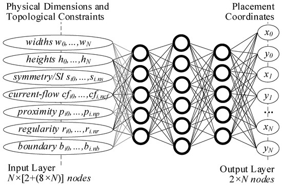
Figure 1.
ANN architecture used to solve the map from the physical dimensions and topological constraints to the placement coordinates. N represents the maximum number of circuit devices supported by the model.
2. Related Work and Contributions
Some of the recent ML applications for analog IC layout include building block recognition from circuit netlists in order to build the circuit’s hierarchy automatically [16], generation of wells during layout design that imitate human-designer choices [17], or even assistance/guidance for traditional path-finding routing algorithms [18]. In the particular case of analog IC placement, a straightforward fully supervised ANN that reproduces the layout patterns of a dataset of legacy placement solutions was proposed [10]. In [11], it was enhanced, providing a multi-circuit model that distinguishes between topologies by describing the topological constraints at the ANN’s input layer. Still, both models are highly dependent on the description of the circuits’ traits on the model’s input layer, preventing them from scaling for circuits with a larger number of devices than those found in the dataset. Therefore, an attention-based graph-to-sequence model was recently proposed, where the encoder-decoder architecture is scalable and invariant to the order in which the devices are provided at the input layer. These unsupervised placement techniques have proved to compete or outperform those generated by state-of-the-art optimization-based placement approaches in [12]. Note that the DL models produced these results in milliseconds, while the optimization techniques took from several seconds up to several minutes, thus, establishing the DL approach as a competitive alternative to the more traditional methods. Nonetheless, due to the intricate formulations required for efficient training of a DL model, only fundamental topological constraints were effectively supported, i.e., symmetry, proximity, and current-flows.
Supporting a broader set of topological constraints is mandatory to tackle a more comprehensive set of industry-standard analog IC design cases and produce aesthetic-wise solutions for the circuit designer. However, their implementation in DL-based tools is not trivial. Therefore, the major contributions of this work are:
- In this paper, differentiable implementations of boundary, regularity, and SI constraints are formulated for the first time in the literature. These are inherently model-independent, i.e., they can be used to train simple models, such as the multilayer perceptron [11], or even complex encoder-decoder architectures [12];
- Existent automatic approaches for analog IC placement that focus on retargeting from legacy designs/templates [3,4], or even ML-based approaches [10], use previously designed placement solutions (layouts) that comprise expert design knowledge. These examples are used as a surrogate for the explicit definition of the constraints to be met. However, legacy layouts containing robust implementations of the abovementioned constraints are scarce and expensive to obtain, and thus, here, the model’s training requires only sizing data, which is way easier to produce, and the model is focused on complying with the explicitly and efficiently described topological constraints. When compared with optimization processes with several topological constraints [1,2], which also explore the possibility of explicitly defining the constraints to be met, the inherent time-consuming optimization cycles are bypassed by the use of deep models. This is, once the model is fully trained, it can produce several valid solutions for a singular problem at push-button speed through its generative characteristics;
- The novel formulations for the boundary, regularity, proximity, and SI constraints are used to train a model that produces placement solutions from scratch at push-button speed for several state-of-the-art block-level analog IC structures, including circuit topologies and technology nodes not used for training, ultimately proving its generalization capabilities.
3. Unsupervised ANN Model with a Broader Topological Constraints Coverage
The general architecture of the proposed ANN model was previously illustrated in Figure 1.
3.1. Notation
Table 1 introduces the notation used through this document.

Table 1.
Notation.
3.2. Input Vector Features
As in its baseline implementation, the model inputs the scaled width/height of the physical implementation (bounding box dimensions) of each device composing the circuit, i.e., a vector of size 2N, where N is the number of devices within that circuit topology, resulting from flattening the device size dimension matrix . Additionally, as thoroughly described in [11], symmetry (that restricts two devices to a mirrored placement along a symmetry axis (SA)), proximity (that describes groups of devices that should be placed closely), and current-flow (that force a monotonic path between the different devices composing the ‘current-flow’) requirements are passed to the ANN by three N × N unweighted adjacency matrices: , and respectively. This work proposes the use of five more matrices to encode the boundary (), regularity (), and SI constraints (). While the sets of topological constraints used for the circuit topologies under study in this work were specified by experienced analog designers, these can be obtained directly by using works that automate their extraction process. These works can be either based on deterministic approaches [19,20], or, as developed recently, by using graph-based ML techniques [16,21,22]. Given the circuit’s sizing and the different constraint graphs, the model is trained to output a placement that fulfills the specified constraints. The placement is output as a long vector, which can be interpreted as an matrix , whose columns correspond to each devices’ coordinates in the and axis respectively.
3.3. Boundary
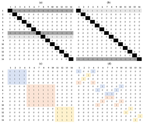
This constraint leads to easier routing access to the interfaces and fewer parasitic interactions, as shown in Figure 2b. A device with a boundary constraint must be placed between the remaining devices of the circuit and the “virtual” enclosing shape that contains all the devices, and, since this verification must be made in one of the four directions, the boundary error is divided into two axes, and . The matrices and encode the boundary constraint graphs for the and y axis respectively. Figure 3a,b show the and matrix respectively for the circuit shown in Figure 2.
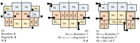
Figure 2.
Three symmetric placements of the generic circuit: (a) Devices connected to the input/output ports are placed inside the circuit layout; (b) devices are placed within the circuit boundary and three horizontal regularity constraints are implemented; (c) two symmetry islands are formed.
In practice, the and matrices encode an ordering along each axis, where encodes that device ’s maximum coordinate should be greater than ’s maximum coordinate, and an analogous meaning is given to . On the other hand, encodes that device ’s minimum coordinate should be lesser than ’s minimum coordinate, and an analogous meaning is given to . Thus, if device should be on the top boundary, then . Or if device should be on the left boundary, then .
Thus, to estimate the boundary error relative to the axis, the TopTop and BottomBottom errors between each device pair must be considered, each respectively represented by and , calculated through:
where corresponds to the vector containing the minimum coordinate of each device in the evaluated placement, defined as , and corresponds to the maximum coordinate vector defined a .
Similarly, for the axis, the RightRight and LeftLeft errors between each device pair, represented by and respectively, are given by:
where corresponds to the vector containing the minimum coordinate of each device in the evaluated placement, defined as , and corresponds to the maximum coordinate vector defined as .
Finally, another factor must be considered to maximize the boundary constraint’s effectiveness: whether a device is located between a boundary-constrained device and its objective (the placement’s boundary). This can be estimated by measuring the overlap between the devices’ projections in the axis perpendicular to the corresponding boundary axis for every device pair with an ordering error greater than zero (i.e., or or or , since this means that device is closer to the objective boundary than , and it must be checked whether it is blocking device ’s path).
To measure the overlap between each device pair’s projections, consider the distance that separates the opposing faces of the two rectangles. For example, matrix measures, for every pair of devices and , the distance between device ’s maximum coordinate face and device ’s minimum coordinate face. Resulting in four matrices, two for each axis: and :
The matrices and that define the measured distance to solve the overlap in each axis are given through:
where is the column vector containing the devices’ heights given by , is the column vector containing the devices’ widths given by and the four matrices , and are scaling weights that function as a soft minimum for the distance between the devices’ opposing faces in each direction, and are defined by:
The use of these scaling weights was introduced in [11], where it is explained in detail, and results in an output with a value between the minimum term and the maximum term, but, proportionally closer to the minimum term, such that when the minimum term approaches , its weight approaches .
Thus, given and , the two matrices, and that evaluate how much devices stand in the way of the boundary constrained devices are given by:
The inclusion of these two errors results from a gradient-aware approach since the objective of the boundary error is not only to identify situations where the constraint is fulfilled but also to, given two distinct placements, rank them faithfully to a designer’s preferences. Locally, this results in defining the function’s gradients and information regarding how to update a placement to correct its errors intelligently. In particular, this added overlap error results in a gradient that pushes devices away from the path of the boundary-constrained devices, resulting in cooperative behavior. Figure 4 shows an example placement where the device should be placed in the top boundary, resulting in three distinct errors , , and . Note that no error exists between and despite the existing horizontal overlap between them since there is no error, thus the max function from Equation (11) returns 0 and . Intuitively, does not stand between and its objective (the top boundary), thus, it should not be pushed away.
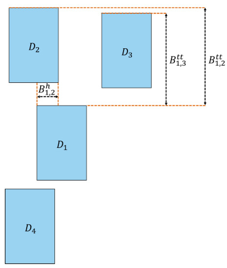
Figure 4.
Example placement where device should be placed in the top boundary, resulting in three distinct errors , , and . Note that no error exists between and despite the existing horizontal overlap between them since is not closer to the top boundary than .
The pairwise boundary error is calculated via:
Finally, this pairwise error could then be properly normalized and pooled through the methods discussed in [12], resulting in a final error .
3.4. Regularity
This constraint arranges the devices into regular layout structures such as rows and columns, often resulting in a compact and meaningful layout, as shown in Figure 2b. The regularity constraint is split into two constraints, one for each axis, and . The regularity constraint applied to the axis constrains device pairs to be vertically aligned, i.e., their centroids should have the same coordinate. Whereas the regularity constrains the pair’s centroids to have the same coordinate. For a given axis, the regularity axis between every pair of devices can be determined by calculating the pair’s centroid’s and position through and :
where and each respectively contain each device’s width and height and are defined as .
After calculating each regularity column and row axis between each pair of devices, given by and respectively, the errors and that measure the deviation between each device to its correspondent column and row axis per pair is calculated, using:
where and are the adjacency matrices of the graphs that encode the column and row regularity constraints respectively. These graphs encode, for a pair of devices and , whether they should be aligned over a vertical or horizontal axis, respectively. Figure 3c shows the row regularity constraint graph’s adjacency matrix for the placement in Figure 2b.
Note how the regularity errors calculated in (16) and (17) measure, for each device pair and , their distance to the pair’s centroid given by or . The alternative would be to directly calculate the distance between each device’s centroid through . However, experimentally, the used errors proved to be more stable. For the same placement, the alternative errors will measure a higher value than the centroid error proposed. Thus, considering the use of momentum-based optimization algorithms (e.g., Adam), the devices will build more momentum and are more likely to overshoot their target and oscillate around the minimum. Whereas the centroid approach presents a common goal for both devices, a “compromise”. That way, the devices will not build as much momentum and are more likely to stabilize around the minimum.
Given the constraint’s pairwise and errors, the final pairwise regularity error is given by:
Finally, this pairwise error can then be normalized appropriately and pooled through the methods proposed in [12], resulting in the final constraint error .
3.5. Relative Proximity
In the boundary error, the overlap error components from Equations (5) and (6) were proposed to make unconstrained devices aware of the constrained devices’ objectives, inducing a collaborative behavior. Similarly, in order to encourage the model to group devices in the same symmetry group in an island (i.e., there is a contiguous shape that can contain all devices in the same symmetry group while not containing any device outside of the group), the implementation of the proximity constraint proposed in [11,12] was updated to behave in the same cooperative manner and used in the SI error to promote island formation. Additionally, note how in past works [12], all of the symmetry, current-flow, and overlap constraints can be satisfied, i.e., their error can be 0. The same, however, is unlikely to happen to the proximity error since the pairwise proximity error is only zero if the two devices are touching each other. This is an unnecessarily strict constraint that actively promotes overlap. A possible approach to turn this constraint satisfiable is to define a maximum threshold distance, under which the proximity error is zero, however, the size of this threshold would be, in practice, a hyperparameter to be optimized, and consequently, subject to overfitting.
Instead, a different approach was taken: the definition of proximity group was changed to a relative sense instead of an absolute one. In this implementation, the devices that form a proximity group (symmetry groups share proximity constraints as well, meaning that all symmetry groups are a proximity group) should be closer to each other than they are to all other devices. Thus, the measured error estimates how close, on average, device is to all devices that do not belong to its proximity group compared to devices that do belong to the same symmetry group. To estimate the error associated to this constraint, first it is necessary to estimate the effective minimum distance (EMD) between every pair of devices, as defined in [12]. The distance measured by this metric corresponds to the minimum distance between any two points belonging to each rectangle (device). The pairwise EMD is represented by the matrix . Given this, the multi-dimensional matrix measures, for a triplet of devices , , and , how closer is device to j than it is to , through:
Note how the compared distances are those between devices in the same proximity group (represented by the term ) with those between devices not in the same proximity group (represented by the term ). To measure the pairwise island formation error, the relative distance matrix must be first filtered for only occurrences where , i.e., , and then averaged over the number of devices with which device does not have a proximity constraint:
By considering a relative definition of proximity, not only does the constraint become satisfiable, but also the devices start behaving cooperatively. Instead of only pushing devices in the same proximity group close, the proximity error now pushes the devices not proximity-bounded away, opening space for the proximity-bounded devices to get close to one another. This is especially important because of the overlap error that often stops other constraints from fulfilling themselves, resulting in a local minimum around which the system oscillates. It should also be highlighted that this change comes at a computational cost, increasing the constraint’s complexity from to Finally, and as before, this pairwise error can then be adequately normalized and pooled through the methods proposed in [12], resulting in the final constraint error .
3.6. Symmetry Island
The SI groups symmetric devices are close to each other, minimizing their mismatch. Therefore, multiple SA are considered, as well as hierarchical symmetry, as shown in Figure 2c. The SI error is separated into two different calculations, the error related to the intra-group interactions and the error related to the axes that separate two different symmetry groups. Thus, this approach is limited to two hierarchical levels of symmetry, but unlimited symmetry axes are supported.
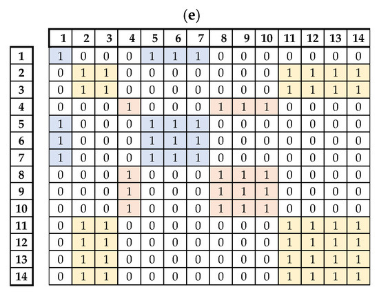
To identify the SI constraints, two different matrices are used: one, the symmetry relations matrix , to identify pairs of devices that are symmetric to one another in relation to any of the SA in the circuit; and a second, the symmetry group matrix , that signals whether two devices share the same SA set, where the SA set of a device is the set of SAs in relation to which the device is symmetric to another. For example, in Figure 2c, three Sas are marked in a dashed line, these can be denominated, from the left to the right: , and . For device , its SA distribution is the set since it is symmetric to itself in relation to and symmetric to in relation to . By defining the SA sets of each device, it is possible to conclude that devices M1, M5, M6, M7 all share the same SA set and thus, belong to the same symmetry group. Figure 3d,e show the two matrices and for the circuit shown in Figure 2.
Since this implementation is limited to two hierarchical levels of symmetry, a device can at most have two symmetry constraints, i.e., . This makes it possible to separate the constraints into two levels, intra-group constraints and inter-group constraints. Intra-group constraints are identified for bounding two devices of the same symmetry group, whereas inter-group constraints bound devices in different symmetry groups.
3.6.1. Intra-Group Axis
For each device, the coordinate of its intra-group symmetry relation is defined in the vector , given by:
where identifies the intra-group relations. By adding the term , a 1 is added to the main diagonal if the corresponding device has an intra-group symmetry constraint. Then the dot product adds the coordinates of the devices’ centroids, which when halved gives the pair’s centroid.
It is possible to build a three-dimensional matrix that for a device , the matrix . Thus, can be seen as a stack of matrices where each layer is filtered such that only the relations relative to the group to which device belongs to are considered (i.e., only consider edges to and from a device in the group). It is important to define this matrix so that the number of symmetry constraints associated to each SA can be accurately calculated. One naïve approach to defining the number of constraints associated with each SA is through the matrix, where for each device, the number of elements in its group would be counted as the number of constraints. For example, for device , its group is defined by the set with cardinality 4, however, since devices and are symmetric to one another, then only 3 symmetry constraints are associated to this intra-group axis. This matrix is estimated via:
Now, a matrix whose values are 0 if and otherwise, its values are the x coordinates of the symmetric pair’s centroid. The values of and are used to compute the matrix through:
The reference symmetry axis for each device, represented by the vector , is computed through:
where the term adds, for each layer in , all values in the upper triangular region of the matrix, which corresponds to the different coordinates of the centroids of all devices that belong to the same symmetry group as device . Then, the term computes for each device , how many symmetry constraints are being considered to properly average out the group’s centroid’s coordinate.
The pairwise error associated with the deviation of a pair’s symmetry axis with its reference, represented by , can be thus estimated via:
The pairwise error associated to the vertical misalignment between an intra-group symmetric pair is given by:
3.6.2. Inter-Group Axis
Similarly, the inter-group pairwise error associated to the deviation of the symmetry axis from the mean is calculated by first estimating, for each device, the coordinate of its symmetry axis with a device from another group , then estimating, for each device, the symmetry constraints between devices in its group with devices from another group , then calculating and the same way they calculated for the intra-group constraints, and finally, calculating the error matrix :
where in Equation (28), the term considers relations to outer-group devices from group devices, and the term considers the opposite.
The pairwise error associated to the vertical misalignment between an inter-group symmetric pair is given by:
The pairwise error associated to the symmetry island constraint is given by:
Finally, this pairwise error can then be normalized and pooled through the methods proposed in [12], resulting in the final constraint error . It should be noted that devices in the same symmetry group form a clique in the proximity constraint graph, thus, these groups will tend to form islands.
3.7. Loss Function
The deep model is ultimately trained to minimize a loss function whose inputs are the placement of the devices (i.e., the model’s output), the circuits’ constraint graphs, and respective sizing (i.e., the model’s inputs). This loss, shown in Equation (34), accounts for the satisfiability topological constraints considered, i.e., proximity (P), symmetry/SI (SI), current-flows (CF), boundary (B), and regularity (R). Still, two other metrics are also utilized to regulate the quality of produced layouts, i.e., overlaps and wasted area (WA and O, respectively). The total loss is then given by the weighted sum of each of these constraint losses, where the wa,pg,si,cf,o,bou,reg variables in Equation (34) represent said weights. Note that each of these constraint-specific losses is calculated in function of the circuit’s sizing (matrix ), its positional constraints (specified by the graphs , , , , , , ) and the produced placement (matrix ). Moreover, by using this unsupervised formulation, the model can be easily trained with unlabeled data, reinforcing its generalized application.
4. Experimental Results
The methodology was coded in Python using PyTorch ML library, and demonstrated with a dataset containing sizing solutions (split into training, validation, and test) for different state-of-the-art amplifiers on two foundries/nodes: the voltage-combiners (VC)-biased amplifier [23] (VCB, umc130), the folded VC-biased amplifier [24] (FVC, umc130, and tsmc65), and the VC-biased single-stage operational transconductance amplifier [25] (VCOTA, umc130), as shown in Table 2. Note that FVC in tsmc65 node was kept for validation and test only. The largest circuit is the VCOTA with 22 devices, whose schematic is illustrated in Figure 5. For it, 11 symmetry pairs were set by an experienced IC designer, 12 current-flows, 6 boundary constraints, 5 regularity constraints (row only), and 15 proximity constraints, as detailed in Table 3. This procedure was performed for the remaining amplifiers, with VCB being the only case study with SIs. Additionally, to balance the dataset, the sizing solutions of FVC were augmented by shuffling the order of the devices. To place larger analog circuit/system topologies, this work can be directly applied to each of the sub-blocks of the system, which, when placed, would be assembled at the top level given a set of topological constraints. As an alternative, the methodology could be used to place the entire complete mixed-signal or system in one single step, the major drawback being the deep model’s training which would escalate proportionally.
Table 2.
Dataset details.
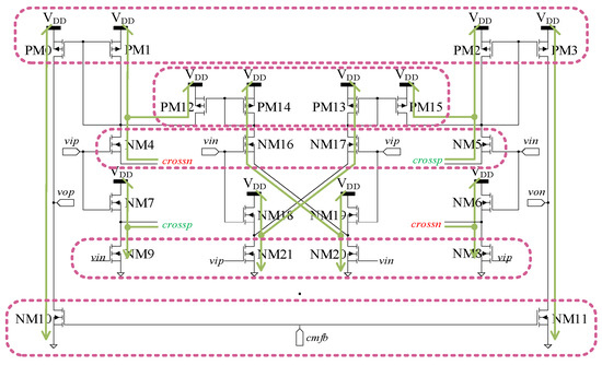
Figure 5.
Schematic of the VCOTA [25]. Current-paths highlighted in green and row regularity constraints highlighted in pink.
Table 3.
List of topological constraints specified for the VCOTA.
The model’s input vector has size 3916, and the weights of Equation (34) were empirically chosen and set to: wa = 0.1, ws = 95, wcf = 80, wbou = 20, wreg = 2, wo = 90, and wpg = 25. The ANN model comprises 5 hidden layers (with 5000/2500/1000/250/100 neurons each) and 1 output layer (44 nodes). The model was trained for 1000 epochs using Adam optimizer, and its parameters were set to: α = 0.001, = 0.9, and = 0.999. A batch size of 500 samples was adopted, and dropout with a drop rate of 0.2 was used to prevent overfitting. The activation function used was the exponential linear unit (ELU) and linear function in the output layer. Table 4 fully details the train, validation, and test set errors. As observable, the test set errors are similar to those obtained on validation, with only a significant difference in the current-flow constraints on VCB and VCOTA. Moreover, its generalization ability is observed on FVC (tsmc65), with errors even lower than validation circuits. Figure 6 shows that the ANN is producing workable solutions.
Table 4.
Train (TrE), validation (VaE), and test (TeE) errors.
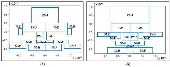
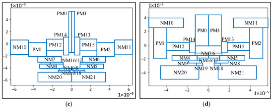
Figure 6.
Test set predictions: (a,b) FVC (tsmc65); (c,d) VCOTA.
Finally, to further demonstrate the value of this work, the proposed approach’s performance was compared to a human expert designer. In this experiment, a human-designed placement for the VCOTA architecture was compared to an automatically generated placement using the approach here proposed. The ANN generated, for a single sizing, 500 different predictions, by shuffling the order of the devices in the input layer. Due to the batch capabilities of the model, the time required for this process is in the order of milliseconds (push-button speed). The best prediction was selected as the final solution produced by the ANN. The two final placements are shown side-by-side in Figure 7. Table 5 compares the numeric values for the compactness, proximity, current flow, regularity, and boundary errors for both solutions. Since the post-processing fixes overlaps and symmetry errors, these are zero and are not compared. Still, no major importance is given to the compactness comparison, as the remaining common-mode feedback circuitry used to bias the original circuit (and fill the empty spaces in the layout) were not included in this work. Nonetheless, in every metric, the automatic approach improves upon the human-designed floorplan, presenting decreases of up to 15-fold in the case of the current-flow error. Overall, the automatic approach is capable of carefully balancing all the different constraints, resulting in a placement with around 70% improvement over the human-designed solution.
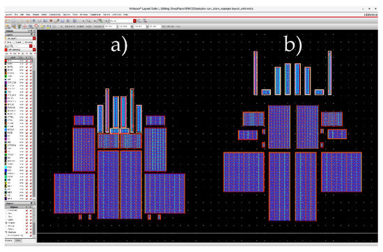
Figure 7.
Placements generated for the VCOTA: (a) generated by this work, (b) designed by a human expert designer [25].
Table 5.
Comparison of the automatically produced and human-designed floorplan solutions.
5. Discussion
Reliable automatic placement tools must support a broad set of topological constraints to tackle industry-standard analog IC design cases and produce aesthetic-wise solutions for the circuit designer. This paper proposes different model-independent and differentiable implementations of boundary, regularity, and SI constraints. The proposed constraints not only enforce the correct placement of the devices but were also designed to maximize the training of DL models. Their design was aware of the gradient produced and used matrix representation for improved performance using hardware parallelization (GPUs). The proof of concept was made with an ANN trained on sizing data of three different state-of-the-art amplifiers, generating workable solutions at push-button speed.
Even though the methodology proposed in this manuscript is tested in a family of state-of-the-art amplifiers, it can be applied to any real circuit class as long as there are well-defined topological constraints (i.e., symmetry pairs, current-flows, proximity, boundary, etc., constraints) for the circuit topologies within that class. If no topological constraints are requested, the deep models will still attempt to minimize the layout’s wasted area/compactness and the overlap among devices, and components of the placement loss indicated in Equation (34). However, the resulting solution may not be meaningful for the circuit designer, as no criteria to place the devices with respect to each other is being set. The experiments carried intend to show that if the deep model is trained in a dataset that shares some of the characteristics regarding topological constraints’ fulfillment of the circuit topologies to be generated, the acquired knowledge can be reused and generalized.
Even if the placement of a relatively small analog integrated circuit block is not extremely time-consuming, once several performance figures have to be considered its complexity increases immensely, and an optimal floorplan solution may not exist due to the inherent tradeoffs. Moreover, analog IC design is characterized by non-systematic re-design iterations, most of which impact the layout design, requiring partial or complete floorplan re-design. By using deep models, these floorplans can be generated instantly, while the human-designed floorplan may take from dozens of minutes to a couple of hours. These times are multiplied through every re-design iteration further conducted on a design.
Author Contributions
Conceptualization, A.G., N.L. and R.M.; methodology, A.G. and P.A.; software, A.G. and P.A.; validation, A.G. and P.A.; investigation, A.G. and P.A.; data curation, A.G. and P.A.; writing—original draft preparation, A.G. and P.A.; writing—review and editing, N.H., N.L. and R.M.; visualization, A.G. and N.L.; supervision, N.H., N.L. and R.M.; project administration, R.M.; funding acquisition, R.M. All authors have read and agreed to the published version of the manuscript.
Funding
This work is funded by FCT/MCTES through national funds and when applicable co-funded EU funds under the project UIDB/50008/2020 (including internal research project LAY(RF)2/X-0002-LX-20), and Research Grant FCT-SFRH/BD/07123/2021.
Data Availability Statement
Data available on request due to restrictions.
Conflicts of Interest
The authors declare no conflict of interest. The funders had no role in the design of the study; in the collection, analyses, or interpretation of data; in the writing of the manuscript, or in the decision to publish the results.
References
- Lin, P.H.; Chang, Y.W.; Lin, S.C. Analog Placement Based on Symmetry-Island Formulation. IEEE Trans. Comput. Des. Integr. Circuits Syst. 2009, 28, 791–804. [Google Scholar] [CrossRef]
- Patyal, A.; Chen, H.M.; Lin, M.P.H.; Fang, G.Q.; Chen, S.Y.H. Pole-Aware Analog Layout Synthesis Considering Monotonic Current Flows and Wire-Crossings. IEEE Trans. Comput. Des. Integr. Circuits Syst. 2022, 42, 266–279. [Google Scholar] [CrossRef]
- Wu, P.H.; Lin, M.P.H.; Chen, T.C.; Yeh, C.F.; Li, X.; Ho, T.Y. A Novel Analog Physical Synthesis Methodology Integrating Existent Design Expertise. IEEE Trans. Comput. Des. Integr. Circuits Syst. 2015, 34, 199–212. [Google Scholar] [CrossRef]
- Pan, P.C.; Chin, C.Y.; Chen, H.M.; Chen, T.C.; Lee, C.C.; Lin, J.C. A Fast Prototyping Framework for Analog Layout Migration with Planar Preservation. IEEE Trans. Comput. Des. Integr. Circuits Syst. 2015, 34, 1373–1386. [Google Scholar] [CrossRef]
- Han, J.; Bae, W.; Chang, E.; Wang, Z.; Nikolic, B.; Alon, E. LAYGO: A Template-and-Grid-Based Layout Generation Engine for Advanced CMOS Technologies. IEEE Trans. Circuits Syst. I Regul. Pap. 2021, 68, 1012–1022. [Google Scholar] [CrossRef]
- Unutulmaz, A.; Dündar, G.; Fernández, F.V. Template Coding with LDS and Applications of LDS in EDA. Analog. Integr. Circuits Signal Process. 2014, 78, 137–151. [Google Scholar] [CrossRef]
- Afacan, E.; Lourenço, N.; Martins, R.; Dündar, G. Review: Machine Learning Techniques in Analog/RF Integrated Circuit Design, Synthesis, Layout, and Test. Integration 2021, 77, 113–130. [Google Scholar] [CrossRef]
- Mina, R.; Jabbour, C.; Sakr, G.E. A Review of Machine Learning Techniques in Analog Integrated Circuit Design Automation. Electronics 2022, 11, 435. [Google Scholar] [CrossRef]
- Gusmão, A.; Passos, F.; Póvoa, R.; Horta, N.; Lourenço, N.; Martins, R. Semi-Supervised Artificial Neural Networks towards Analog IC Placement Recommender. In Proceedings of the IEEE International Symposium on Circuits and Systems (ISCAS), Seville, Spain, 12–14 October 2020. [Google Scholar] [CrossRef]
- Guerra, D.; Canelas, A.; Póvoa, R.; Horta, N.; Lourenço, N.; Martins, R. Artificial Neural Networks as an Alternative for Automatic Analog IC Placement. In Proceedings of the SMACD 2019—16th International Conference on Synthesis, Modeling, Analysis and Simulation Methods and Applications to Circuit Design (SMACD), Lausanne, Switzerland, 15–18 July 2019. [Google Scholar] [CrossRef]
- Gusmão, A.; Póvoa, R.; Horta, N.; Lourenço, N.; Martins, R. DeepPlacer: A Custom Integrated OpAmp Placement Tool Using Deep Models. Appl. Soft Comput. 2022, 115, 108188. [Google Scholar] [CrossRef]
- Gusmão, A.; Horta, N.; Lourenço, N.; Martins, R. Scalable and Order Invariant Analog Integrated Circuit Placement with Attention-Based Graph-to-Sequence Deep Models. Expert Syst. Appl. 2022, 207, 117954. [Google Scholar] [CrossRef]
- Wu, I.P.; Ou, H.C.; Chang, Y.W. QB-Trees: Towards an Optimal Topological Representation and Its Applications to Analog Layout Designs. In Proceedings of the Design Automation Conference, Austin, TX, USA, 5–9 June 2016; Institute of Electrical and Electronics Engineers Inc.: New York, NY, USA, 2016. [Google Scholar]
- Sanabria-Borbón, A.C.; Soto-Aguilar, S.; Estrada-López, J.J.; Allaire, D.; Sánchez-Sinencio, E. Gaussian-Process-Based Surrogate for Optimization-Aided and Process-Variations-Aware Analog Circuit Design. Electronics 2020, 9, 685. [Google Scholar] [CrossRef]
- Valencia-Ponce, M.A.; Tlelo-Cuautle, E.; de la Fraga, L.G. On the Sizing of Cmos Operational Amplifiers by Applying Many-Objective Optimization Algorithms. Electronics 2021, 10, 3148. [Google Scholar] [CrossRef]
- Kunal, K.; Dhar, T.; Madhusudan, M.; Poojary, J.; Sharma, A.; Xu, W.; Burns, S.M.; Hu, J.; Harjani, R.; Sapatnekar, S.S. GANA: Graph Convolutional Network Based Automated Netlist Annotation for Analog Circuits. In Proceedings of the 2020 Design, Automation and Test in Europe Conference and Exhibition, Grenoble, France, 9–13 March 2020; Institute of Electrical and Electronics Engineers Inc.: New York, NY, USA, 2020; pp. 55–60. [Google Scholar]
- Xu, B.; Lin, Y.; Tang, X.; Li, S.; Shen, L.; Sun, N.; Pan, D.Z. WellGAN: Generative-Adversarial-Network-Guided Well Generation for Analog/Mixed-Signal Circuit Layout. In Proceedings of the 56th Design Automation Conference, Las Vegas, NV, USA, 2–6 June 2019; Institute of Electrical and Electronics Engineers Inc.: New York, NY, USA, 2019. [Google Scholar]
- Zhu, K.; Liu, M.; Lin, Y.; Xu, B.; Li, S.; Tang, X.; Sun, N.; Pan, D.Z. GeniusRoute: A New Analog Routing Paradigm Using Generative Neural Network Guidance. In Proceedings of the IEEE/ACM International Conference on Computer-Aided Design (ICCAD), Westminster, CO, USA, 4–7 November 2019. [Google Scholar] [CrossRef]
- Eick, M.; Strasser, M.; Lu, K.; Schlichtmann, U.; Graeb, H.E. Comprehensive Generation of Hierarchical Placement Rules for Analog Integrated Circuits. IEEE Trans. Comput. Des. Integr. Circuits Syst. 2011, 30, 180–193. [Google Scholar] [CrossRef]
- Eick, M.; Graeb, H.E. MARS: Matching-Driven Analog Sizing. IEEE Trans. Comput. Des. Integr. Circuits Syst. 2012, 31, 1145–1158. [Google Scholar] [CrossRef]
- Liu, M.; Li, W.; Zhu, K.; Xu, B.; Lin, Y.; Shen, L.; Tang, X.; Sun, N.; Pan, D.Z. S3DET: Detecting System Symmetry Constraints for Analog Circuits with Graph Similarity. In Proceedings of the 25th Asia and South Pacific Design Automation Conference (ASP-DAC), Beijing, China, 13–16 January 2020; pp. 193–198. [Google Scholar] [CrossRef]
- Kunal, K.; Poojary, J.; Dhar, T.; Madhusudan, M.; Harjani, R.; Sapatnekar, S.S. A General Approach for Identifying Hierarchical Symmetry Constraints for Analog Circuit Layout. In Proceedings of the IEEE/ACM International Conference on Computer-Aided Design, Virtual Event, 2–5 November 2020. [Google Scholar] [CrossRef]
- Povoa, R.; Lourenco, N.; Martins, R.; Canelas, A.; Horta, N.C.G.; Goes, J. Single-Stage Amplifier Biased by Voltage Combiners with Gain and Energy-Efficiency Enhancement. IEEE Trans. Circuits Syst. II Express Briefs 2018, 65, 266–270. [Google Scholar] [CrossRef]
- Povoa, R.; Lourenco, N.; Martins, R.; Canelas, A.; Horta, N.; Goes, J. A Folded Voltage-Combiners Biased Amplifier for Low Voltage and High Energy-Efficiency Applications. IEEE Trans. Circuits Syst. II Express Briefs 2020, 67, 230–234. [Google Scholar] [CrossRef]
- Povoa, R.; Lourenco, N.; Martins, R.; Canelas, A.; Horta, N.; Goes, J. Single-Stage OTA Biased by Voltage-Combiners with Enhanced Performance Using Current Starving. IEEE Trans. Circuits Syst. II Express Briefs 2018, 65, 1599–1603. [Google Scholar] [CrossRef]
Disclaimer/Publisher’s Note: The statements, opinions and data contained in all publications are solely those of the individual author(s) and contributor(s) and not of MDPI and/or the editor(s). MDPI and/or the editor(s) disclaim responsibility for any injury to people or property resulting from any ideas, methods, instructions or products referred to in the content. |
© 2022 by the authors. Licensee MDPI, Basel, Switzerland. This article is an open access article distributed under the terms and conditions of the Creative Commons Attribution (CC BY) license (https://creativecommons.org/licenses/by/4.0/).