Article

Exploiting a Deep Learning Toolbox for Human-Machine Feedback towards Analog Integrated Circuit Placement Automation

1
Instituto de Telecomunicações, Universidade de Lisboa, Av. Rovisco Pais 1, 1049-001 Lisboa, Portugal
2
Instituto Superior Técnico, Universidade de Lisboa, Av. Rovisco Pais 1, 1049-001 Lisboa, Portugal
3
Departamento de Informática, Universidade de Évora, Rua do Cardeal Rei, s/n, 7000-849 Évora, Portugal
*
Author to whom correspondence should be addressed.
Electronics 2022, 11(23), 3964; https://doi.org/10.3390/electronics11233964
Submission received: 9 November 2022 / Revised: 23 November 2022 / Accepted: 28 November 2022 / Published: 29 November 2022

Abstract

:
The layout design of analog integrated circuits has been defying all automation attempts, and it is still primarily a handcrafting process carried by circuit designers on traditional layout editing frameworks. This paper presents a toolbox based on deep learning techniques and a sturdy graphical user interface to assist designers during that process. The underlying mechanism of this toolbox relies on a simple pairwise device interaction circuit description, i.e., the circuits’ topological constraints, to propose valid floorplan solutions for block-level structures, including topologies and deep nanometer technology nodes not used for its training, at push-button speed. Despite its automatic functionalities, the toolbox is focused on explainable artificial intelligence, involving the designer in the synthesis flow via filtering and editing options over the candidate floorplan solutions. This constant state of human-machine feedback environment turns the designer aware of the impact of each device’s position change and inherent tradeoffs while suggesting subsequent moves, ultimately increasing the designers’ productivity in this time-consuming and iterative task. Finally, the toolbox is shown to instantly generate floorplans with similar or better constraint fulfilment than human designed solutions for state-of-the-art analog circuit blocks.

1. Introduction

The placement problem of the analog integrated circuit (IC) layout design flow is set to find the locations for the devices/blocks of a given circuit/system topology that minimize different performance figures. The most common performance figures to be minimized are the placement’s area (and thus saving silicon space) and estimates of the interconnect wire length (further improving the circuit’s routability). The final placement must also reflect several topological constraints such as device matching, symmetry and regularity arrangements between two devices/blocks or groups of devices/blocks, or even proximity between any number of circuit elements. These topological requirements are necessary to produce a robust floorplan against process variations and parasitic layout structures. Several other constraints, e.g., thermal gradients or current/signal-flows, can also be considered depending on the target application. Since the quality of the placement solution is highly correlated with the resulting post-layout performance degradation, automatic analog IC placement methodologies have been intensively studied in the past few decades to assist circuit designers [1,2]. However, the layout design of analog ICs has been defying all automation attempts, and it is still primarily a handcrafting process carried by circuit designers on traditional layout editing frameworks. Moreover, changes in the circuit/system topologies, design specifications, or even bias, may annul part of, or all, the previous layout design work, resulting in an iterative and cumbersome task.
Different electronic design automation (EDA) tools for automatic analog IC placement were proposed in the literature, which can ultimately be distinguished by the number of legacy layouts (i.e., a previously designed and validated layout) used to generate the new floorplan solution: (1) generated from topological constraints, where no legacy layouts are used, and every solution is generated by a, usually time-consuming, optimization process operating over a topological [3] or absolute [4] representation; (2) retargeted from a legacy layout or template [5], where a previously produced floorplan of the same circuit is migrated using fast compaction techniques to a new technology node or different devices’ sizes; (3) approaches that attempt to combine the advantages of generation from topological constraints and retargeting from a layout template, which can be helpful inside automatic analog IC sizing methodologies [6,7]; and (4) synthesized by knowledge mining [8], where a library of legacy layouts is decomposed into sub-blocks, and then, the floorplan of the circuit being generated matches them to its own sub-blocks. Commercial solutions have also evolved in the last decade, providing better user-assisted experiences [9]. However, advances in machine learning (ML), including deep learning (DL), created new IC design automation opportunities [10,11]. In the analog spectrum, for automatic circuit sizing, DL models that predict the devices’ sizes when requested for specific circuit performances were recently proposed [12]. Still, DL models that map from devices’ sizes to circuit performances, bypassing expensive simulations, are also attractive solutions [13]. Other recent ML applications include hierarchy and building block recognition from circuit netlists [14]; models that reproduce the layout patterns of a dataset of legacy placement solutions [15]; or even guidance for routing problems [16].
This paper presents a toolbox based on advanced DL techniques and a sturdy graphical user interface (GUI) to assist designers during the analog IC placement task. Despite its fully automatic functionalities, the toolbox is focused on explainable artificial intelligence (AI), involving the designer in the synthesis flow via filtering and editing options over the candidate floorplan solutions, offering a constant state of human-machine feedback. The remainder of this paper is organized as follows. Section 2 overviews the related work and contributions of this work. Section 3 describes the toolbox based on advanced DL techniques. Section 4 presents the experimental results, and Section 5 carries a final discussion of the results and remarks.

2. Related Work and Contributions

Lately, different approaches based on ML models have been proposed to assist IC designers in the analog layout generation task. Some of the current works in this area are attempting to apply graph-based ML techniques to a circuit’s netlist in order to decompose a circuit hierarchically and automatically identify in its structure constraints for different design tasks [14,17,18], e.g., symmetry constraints for placement. In a different direction, conditional generative adversarial networks were developed to automate the process of well design based on previously designed and validated layouts [19]. Towards automatic routing, a variational autoencoder architecture that mimics human guidance in analog IC routing problems was proposed [16]. In the particular case of analog IC placement automation, which is the focus of this work, an initial approach was taken by using mean-field neural networks as planes with a grid where the devices should be placed [20]. The problem is represented by a network of several of these parallel planes, one for each device in the circuit, where each plane has the dimensions of the discrete space in which the devices can be placed. Each edge of the grid is a neuron, and an active neuron represents the position of the bottom-left coordinate of the device corresponding to the plane that the active neuron is part of. However, these models are highly topology dependent, and a new network must be created and trained for each new circuit. In a different direction and to pursue the knowledge mining path, artificial neural networks (ANNs) have been applied towards learning design patterns of thousands of different validated placement solutions for a single topology [15]. The placements differed from each other (while still fulfilling symmetry and current-flow constraints), and the model’s objective was to learn these different design patterns and apply them to new circuit sizing scenarios. The output of the network was the position of each of the circuit’s devices in an R2 plane, and it was trained to minimize the mean squared error (MSE) between the predicted floorplan and its corresponding solution from the training set. Unlike previous knowledge mining approaches [8], this end-to-end approach does not require defining any kind of tie-breaker manually. An ANN trained by an unsupervised topological constraint satisfaction loss function was introduced in [21]. Evaluating whether the predicted placements fulfilled the specified constraints instead of comparing them to legacy data promoted novel yet correct behavior. Additionally, the work introduced circuit topology encodings that enabled the same model to be applied to different circuit blocks, enabling the reuse of the acquired knowledge across the different topologies. Recently, the idea of an attention-based graph-to-sequence model was proposed [22], where the promising encoder-decoder architecture attempts to provide a model not limited by a maximum number of devices, i.e., promoting scalability. This and other DL models have proved to compete or outperform highly optimized placement solutions while producing the results in milliseconds [22]. Finally, extensive reviews on traditional automatic analog placement tools including generation from topological constraints, retargeting from a legacy layout or template or synthesis by knowledge mining are remitted to [1,2].
Following the most recent efforts of applying ML/DL techniques to automate analog IC placement, in this paper, an innovative multi-topology technology-independent DL-based toolbox to assist circuit designers is proposed. Instead of focusing on the underlying ML/DL mechanism, emphasis is given to the implementation of a user-friendly GUI (focused on explainable AI) and input/output interfaces. The GUI involves the IC designer in the synthesis flow via filtering and editing options over the candidate floorplan solutions, offering a constant state of human-machine feedback. Its main contributions can be summarized as follows:
  • The proposed toolbox breaks with recent ML-based analog IC placement approaches [15,20,21,22] by focusing on explainable AI, where the expert designer is involved in the synthesis flow. This is accomplished through its GUI, offering filtering and editing options over the several proposed floorplan solutions. During floorplan design there are several conflicting constraints and objectives, and by providing a tool is in a constant state of human-machine feedback, the impact of each device’s position change and the inherent tradeoffs is instantly presented to the IC designer. Additionally, subsequent moves are also suggested by the tool;
  • The toolbox’s underlying DL model relies on pairwise device interactions, which can encode any of several topological constraints. This feature results in an enhanced generalization, turning it capable of dealing with newer circuit topologies (i.e., circuit topologies not used for its training), unlike approaches based on retargeting from a legacy layout or template or synthesis by knowledge mining that make use of existing target examples in the form of previously designed placement solutions, encoding the knowledge and intuition of the design expert. In those, the legacy examples serve as a surrogate for the explicit definition of the constraints to be met, and the problem is ultimately dealt with in a fully deterministic fashion, where a given circuit is matched to a previously seen design without any innovation or case-specific optimization. Deep Placer’s enhanced generalization simultaneously allows to handle different technology nodes without additional effort;
  • Similar to the approaches based on generation from topological constraints, the toolbox automatically produces placement solutions from scratch. Those works have already explored the possibility of explicitly defining the constraints to be considered within the synthesis process. However, they rely on time-consuming optimization cycles to design each solution. Deep Placer increases designers’ productivity by proposing tens of valid floorplan solutions for a singular block-level analog structure at push-button speed (i.e., bypassing the time required for optimization);
  • Experimental results show that the toolbox produces competitive floorplans compared to human-designed ones while complementing industry automation solutions.
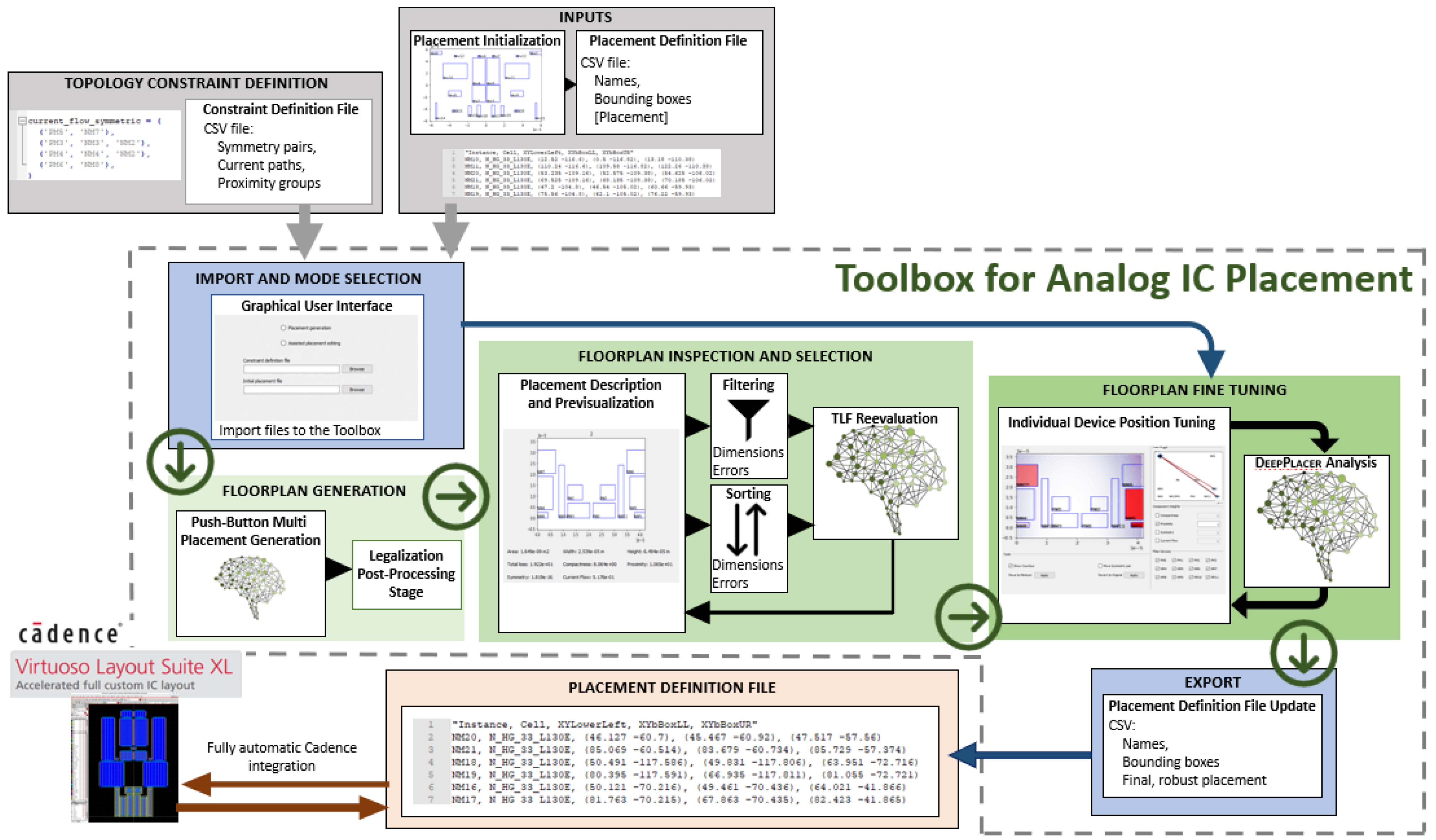
3. Toolbox

The high-level synthesis flow of the proposed toolbox based on advanced DL techniques is illustrated in Figure 1. Its inputs are the topological constraint and devices’ dimensions.

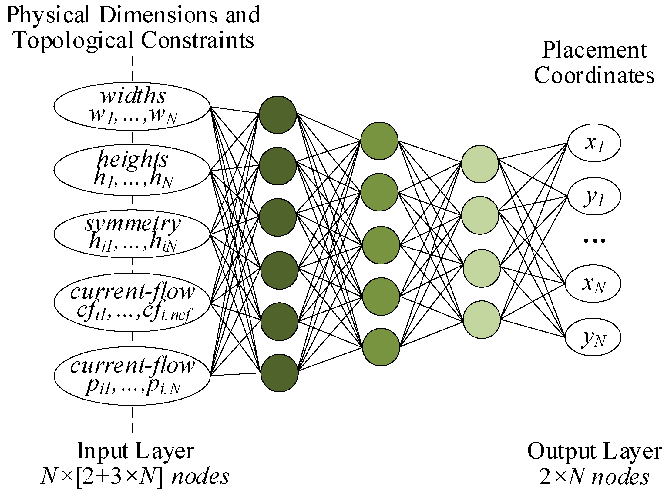
3.1. Underlying DL Model

A DL model, an improved version from [21], with a more abstract constraint codification and graph structure compatibility, generates a set of recommended placement solutions that can be inspected and selected. As in its baseline implementation, the DL model inputs the scaled width/height of the physical implementation (bounding box dimensions) of each device composing the circuit, i.e., a vector of size 2 × N, where N is the number of devices within that circuit topology. Additionally, as thoroughly described in [21], symmetry (that restricts two devices to a mirrored placement along a symmetry axis), proximity (that describes groups of devices that should be placed closely), and current-flow (that force a monotonic path between the different devices composing the ‘current-flow’) requirements are passed to an ANN model by three N × N unweighted adjacency matrices, as illustrated on Figure 2. The trained ANN was composed of 4 hidden layers with 2500/1000/250/100 neurons each. In general, the performance of an ANN on the training set increases with the number of neurons. Note that this is only true for the training set, as increasing the complexity of the model too much may lead to an increase in the validation loss, i.e., overfit. So, in order to find the best model architecture, a small model was initially used and its complexity slowly increased until an increase in the validation loss was observed, meaning the model has begun to overfit, resulting in the final model architecture.
The DL model is ultimately trained to minimize a loss function whose parameters are the placement of the devices, i.e., the output of the model under training, and the circuits’ representation and respective sizing, i.e., the model’s inputs. This topological loss function, shown in Equation (1), accounts for the satisfiability topological constraints considered, i.e., proximity (P), symmetry (S), and current flows (CF). Still, two other metrics are also utilized to regulate the quality of produced layouts, i.e., overlaps and wasted area (WA and O, respectively). Moreover, using this formulation, the model can be easily trained with unlabeled data, reinforcing its generalized application.
l o s s = w a W A + w p g P + w s i S I + w c f C F + w o O
Note that any DL model can be used as long as it supports the input structure, contributing to the tool’s modularity. Alternatively, the tool can also input an initial floorplan solution, i.e., an actual layout. The produced or imported placement can then be analyzed in a user-assisted flow that provides detailed information on constraint satisfaction errors calculated through the developed topological loss function: the total error and the discriminated components. In this placement fine-tuning, a human-machine feedback environment is established, where the impact of each device’s location can be immediately analyzed to understand the tradeoffs of its location in the floorplan, keeping the designers in the loop and aware of the impact of their decisions. Moreover, all constraints are defined as inter-device relations. The error that drives the toolbox can be intuitively visualized in a graph structure that shows the relative position’s error contribution between pairs of devices, enabling the designer to identify critical devices and quickly produce an improved solution.
Multi-topology technology-independent floorplan production is essential to build a competent EDA tool, and thus, the solution adopted was a graph-based description of the constraints that ultimately define the circuit topology in a graph description of the problem. Emphasis is given to interactions between device pairs, resulting in a segmentation of the input into smaller parts. Since graph-encoded features were used, a graph-structured DL model was developed. Additionally, each example’s sizing is independently scaled before being solved, keeping only information regarding the devices’ relative sizes, turning the tool capable of dealing with multiple technology nodes. Finally, the designed TLF is by nature fully unsupervised, turning the model’s training dependent on schematic-level examples only. As sizing solutions are much easier to obtain/produce than floorplans, it grants access to sufficient data to train the model to a competitive level.

3.2. Context for a Human-Machine Feedback Approach

As stated, analog IC placement design is heavily reliant on manual labor. Its flow can be described as a feedback loop, where the designer identifies patterns and tests different topological relations between cells, but whose impact on circuit performances is only known after complete routing and extraction. Naturally, experienced designers have developed intuition in the form of guidelines that should be followed to minimize layout design risks. These guidelines can be interpreted as placement constraints. In [2], eight different constraints were identified, e.g., symmetry, proximity, alignment, current flows, etc. However, by considering some of them, a deeply entangled multi-constraint problem whose complexity increases exponentially with the number of devices must be solved.
Consequently, due to the tradeoffs involved, no single optimal floorplan solution for a given problem exists. The usage of these guidelines has greatly improved human designer performance, but the development of automatic tools that properly interpret them and simulate human behavior has been a challenging research topic. While they are very intuitive for humans, they are hard to translate to an automatic tool in such a way that they maintain their full abstraction, preserving their high applicability and scalability capabilities.

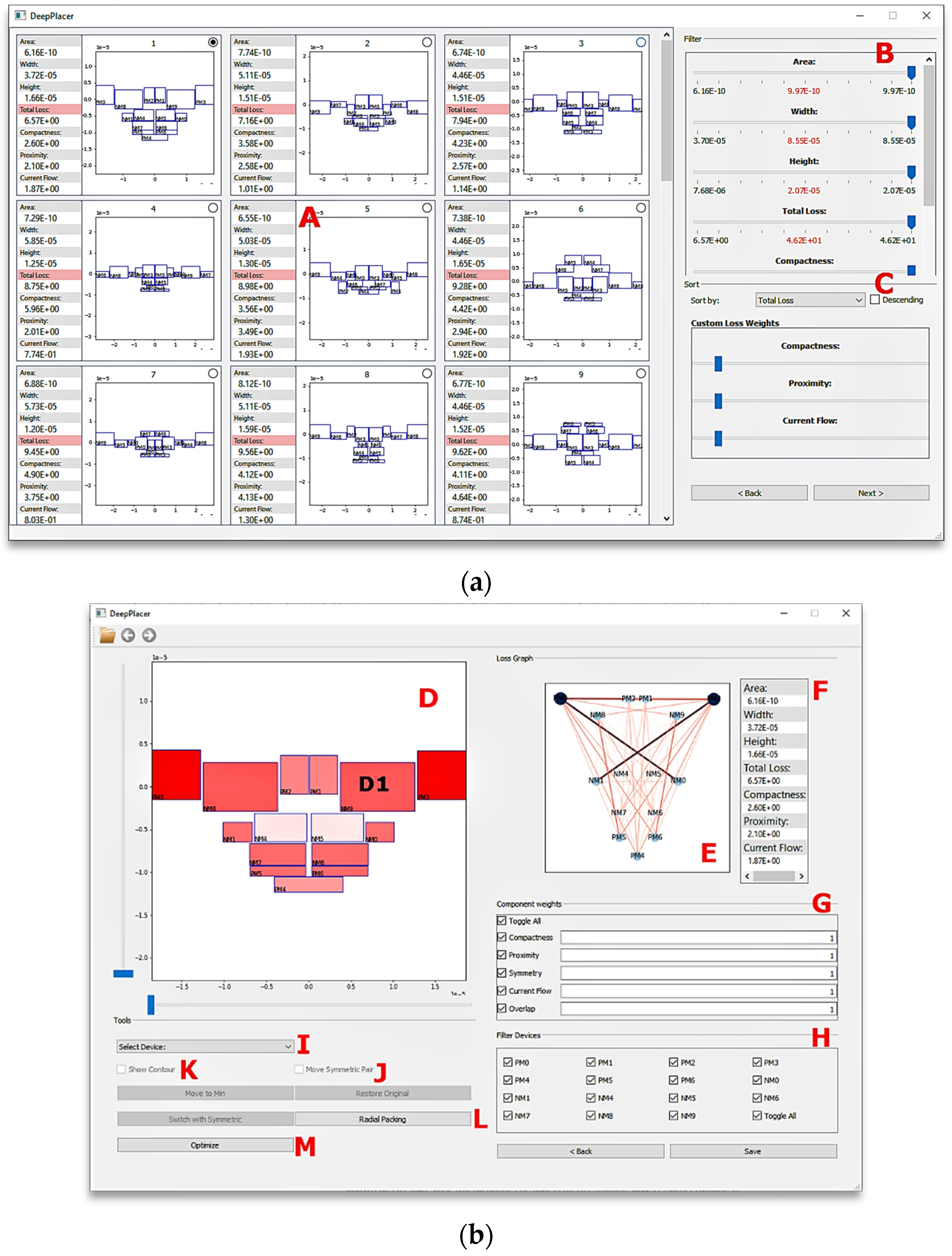
3.3. Fully Automatic and User-Assisted Functionalities

The toolbox relies on an elegant description of intuitive expert-designed guidelines to produce several robust placements at push-button speed. These placement guidelines, detailed in [2], were generated through years of experience and directly impact the placement quality. The toolbox is capable of reproducing expert designer’s patterns that lead to effective placements. This tool’s entire design flow is built around the robustness of the solutions and the design tradeoffs’ impact on them.
It can operate fully automatically, proposing floorplans at push-button speed given the bounding boxes of the circuit’s devices and the set of topological constraints that bind them. Due to the constraints’ complexity, it is common that no solution meets all constraints, and tradeoffs must be made. The toolbox uses a DL to produce a set of recommended placements automatically. The criteria used to evaluate the solutions are also shown, explaining the tool’s design choices. This feedback mechanism identifies, for each device, its location contribution to the overall cost, providing intuition to the designer on the many constraints that the placement is subject to. The designer can then analyze and select one of the placement solutions out of the many produced by the toolbox. Moreover, the feedback mechanism can also guide manual adjustments to the generated floorplans or imported previous designs, keeping the designer informed of the changes’ impact.

3.4. Graphical User Interface

The toolbox’s main interface with the designer is done using the GUI shown in Figure 3. The tool requires a topology-specific file that identifies the devices and their constraints. It also inputs a file with the sizes of the device’s bounding boxes (and optionally their location) and outputs the resulting devices’ locations. The first needs to be crafted manually, while the others are exported/imported automatically from/to Cadence’s Virtuoso layout editor [9].
Figure 3a shows the placement inspection and selection window. Panel A shows a card for each floorplan, containing its previsualization and detailed description: floorplan’s area, width, and height, as well as the total error and the discriminated topological components. Panel B is used for filtering, while panel C is used for sorting. The designer can filter for placement solutions that do not meet any wider-scope criteria. The floorplans can be filtered and sorted by any dimension or constraint satisfaction error. Panel C allows for defining custom TLF weights through which the candidate floorplans will be reevaluated and properly sorted.
Figure 3b shows the placement fine-tuning window, a human-machine feedback environment. In this environment, the designer can inspect the placement via its representation panel (panel D), and then select one of the devices to fine-tune via the combo-box labeled by I. To strategize any change, while no device is selected, the toolbox shows the normalized TLF errors of each device as their filling color (D1). Since all constraints were defined as inter-device relations, the error can be visualized in a graph. Panel E shows the error graph of the circuit. Each node’s/edge’s size and color codify the device’s/interaction’s error, enabling the intuitive interpretation of the error. For more detailed information, panel F shows the error values considering the TLF weights and the selected devices since the influence of any device on the error can be toggled in panel H to discern the interaction causing the error better. Panel G enables the visibility of any TLF error components to be toggled, equivalent to setting the component’s weight to 0. The option of adjusting each weight is also given. The “move symmetric pair” checkbox (J) enables the device’s symmetric pair to be moved symmetrically in case a device is selected for fine-tuning. Once a device has been selected, the errors shown are only those explicitly related to it. For other devices, the error that is shown results from their interaction with the selected device. Meanwhile, panels G and H still serve their purpose of filtering unwanted information, facilitating error interpretation. The toolbox can also superimpose a contour (K) on the placement, indicating, for each point in the 2D plane, the expected normalized error if the device is moved to that position. Finally, a packing procedure (L), along with a local optimization routine (M) are made available as well.

3.5. Applicability

The toolbox relies on a carefully designed multi-topology and technology-independent placement model for analog cells. It is unfeasible to train a model with all the existing circuit topologies on all technology nodes, but the graph-based description of the constraints was carefully conceived to reduce inter-topology variability. While the circuit topology ultimately defines the constraints, the model learns to place the boxes subject to the topological constraints, and not to place a transistor or a capacitor of a specific circuit. Analogously, the constraint satisfaction error calculated through the TLF, evaluates the robustness of a placement through the analysis of these pairwise device interactions, and moreover, device dimensions are scaled per example (unlike usual ML approaches that scale the entire datasets). These considerations promote generalization, enabling an utterly unknown circuit topology or technology to be successfully decomposed into smaller, known device pair-wise interactions. The tool is highly scalable and versatile, capable of dealing with different topologies composed of a varying number of devices.
The toolbox is fully coded in Python and is fully integrated with mainstream deep learning frameworks (Scikit-learn and Py Torch), allowing state-of-the-art performance in designing, training, and usage of the developed ML models. Additional SKILL scripts bridge the toolbox with Virtuoso, producing the toolbox’s inputs directly from the layout editor and using the toolbox’s outputs to set the generated placement back into the layout view. As such, the toolbox is fully and transparently integrated into the design flow.

4. Results

Towards demonstrating the toolbox’s predictive, interactive, and integration capabilities, predictions were generated for two state-of-the-art amplifier circuit blocks. Nonetheless, as long as there are well-defined topological constraints (i.e., symmetry pairs, current-flows, and proximity constraints), Deep Placer can be applied to any circuit class. If no topological constraints are requested, Deep Placer will still attempt to minimize the layout’s wasted area and overlap among devices, i.e., components of the placement loss function adopted and its user-assisted functionalities can be utilized. Still, the resulting solution may not be meaningful for the circuit designer, as no criteria to place the devices with respect to each other were set.
For the placement of larger analog circuit/system topologies, Deep Placer can be directly applied to deal with each of the sub-blocks of a system design, which, when placed, would be assembled at the top level given a set of topological constraints. Nonetheless, the methodology could still be used to place a complete mixed-signal or system design in one single step. Regarding computational efficiency, Deep Placer scales well with an increasing number of devices within a circuit topology, and the mixed-signal or system’s placement would still be outputted within milliseconds. The major drawback will be Deep Placer’s training within a dataset of system designs, whose deep model’s training times will escalate proportionally.

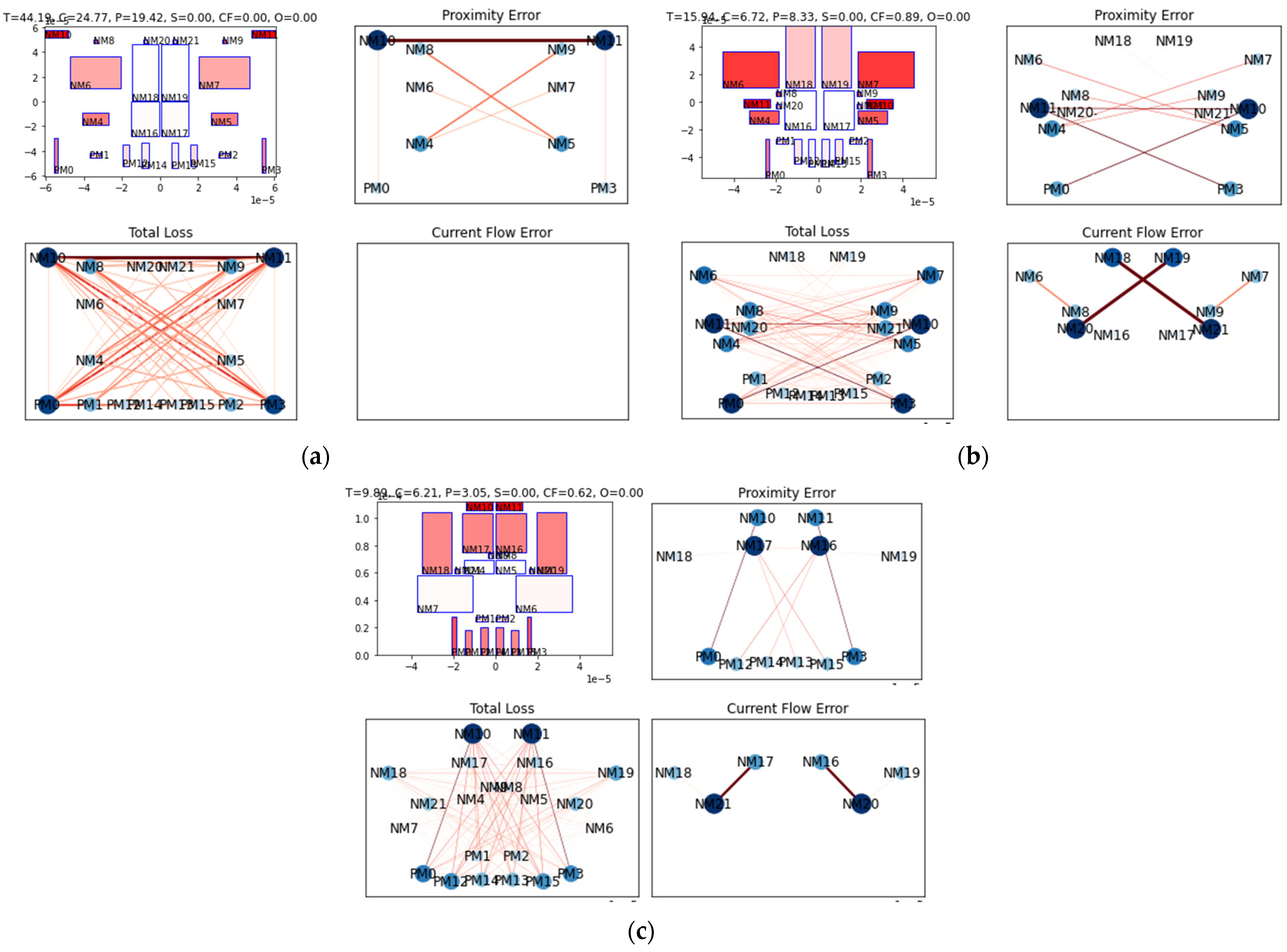
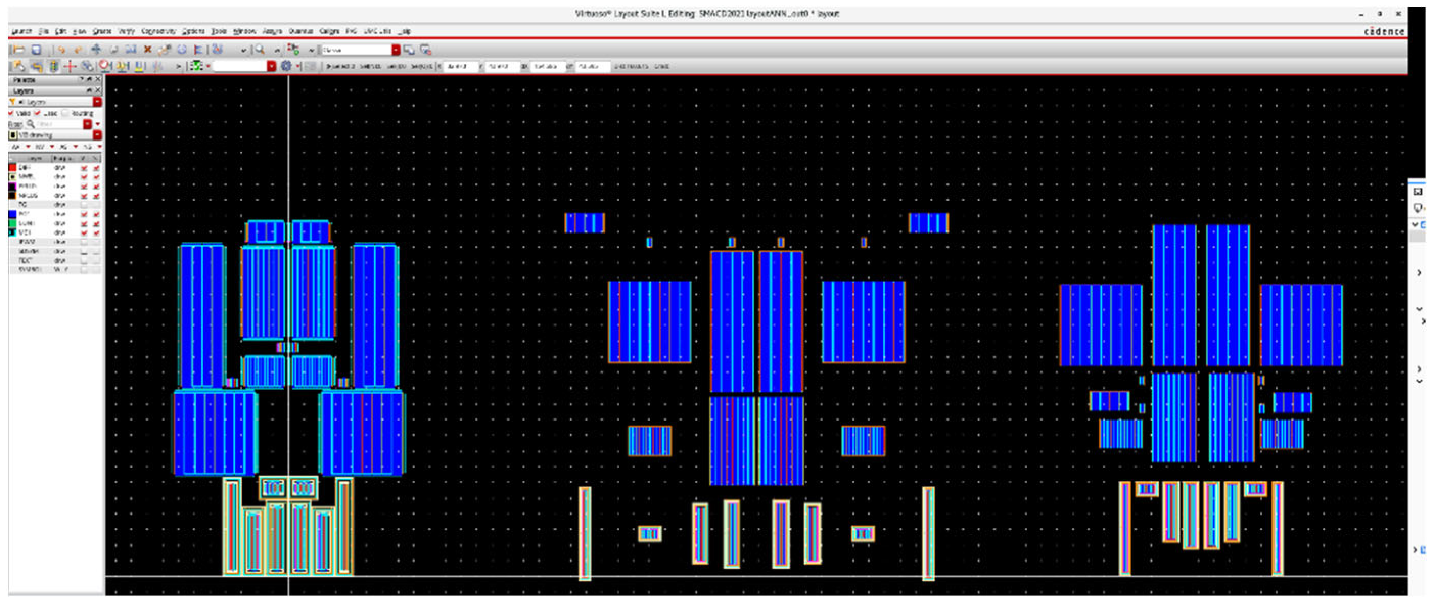
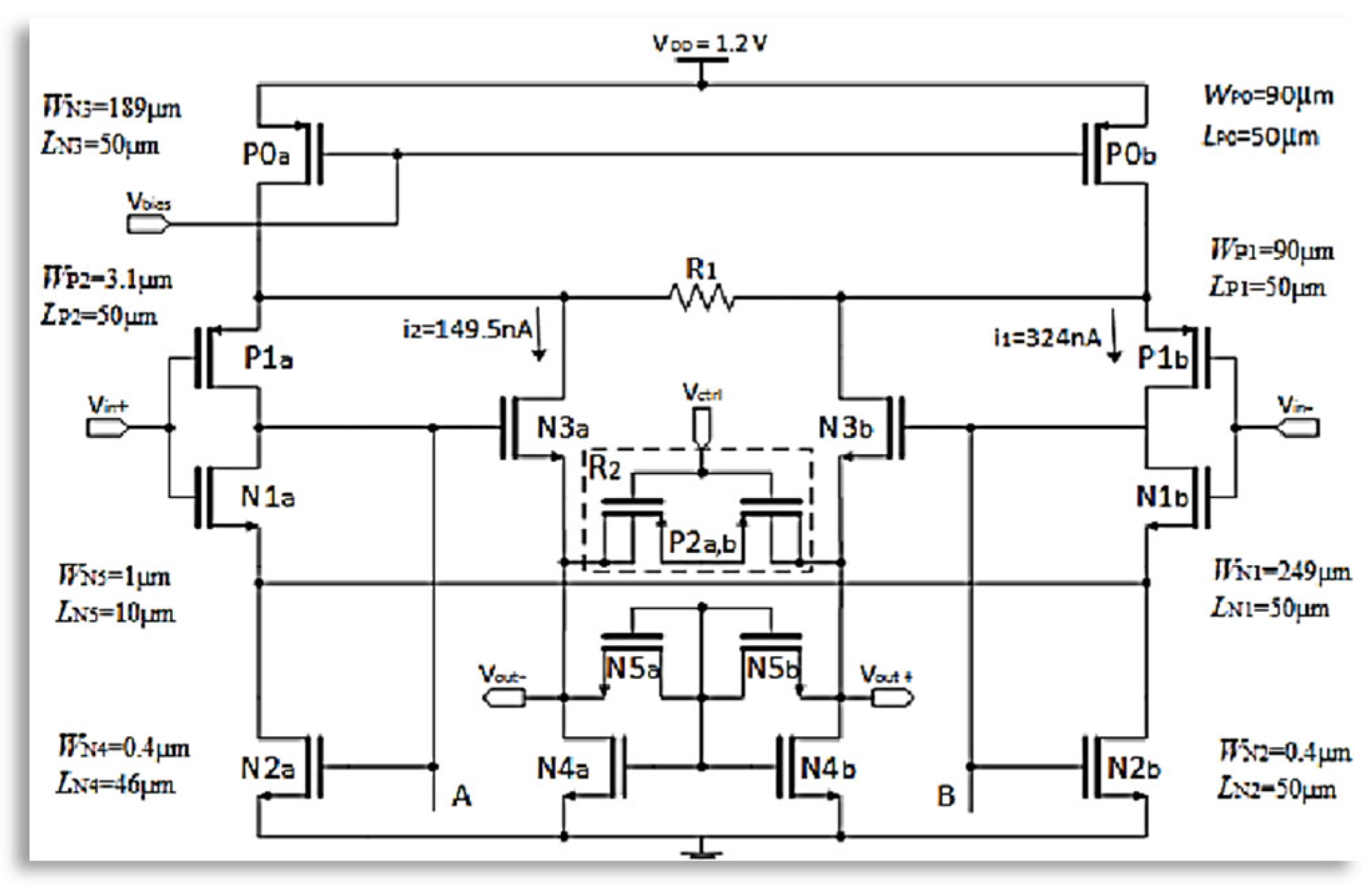
4.1. Current Starving Single-Stage Amplifier biased by Voltage-Combiners

The first case study is the current-starving single-stage amplifier biased by voltage-combiners [23], for a 130-nm technology node, as presented in Figure 4. The toolbox is used to improve the floorplan generated from Virtuoso XL [9], resulting from automatic device instantiation. Results are also compared to the original human-made placement, which provided the topological constraints required for Deep Placer. Even though design engineers specified the topological constraints used in this work, different works are available to extract topological constraints automatically. These works can be based on deterministic approaches [24] that detect symmetries in the circuit or its enhanced versions [25] that further improve symmetry detection by partitioning the circuit in a core and bias sub-circuits, behavioral signal flow analysis and by including some single-ended passive devices. Alternatively, more recently, this task can be based on graph-based ML techniques [14,17,18], as overviewed in Section 2. In summary, any of those methods can feed our deep models in a real-world context application.
Figure 5 shows the placement solutions and the error graphs associated with the total, proximity, and current-flow errors (constraints considered in the manual design). Table 1 shows their numeric mean errors. These errors were calculated using the matrix formulations described in [22]. All the errors are derived from constraints, compactness, proximity, and current flow. As explained in the article, the constraints are described as pairwise constraints, resulting in a constraint graph. For each device in the circuit (equivalent to each node in the constraint graph), an error associated with each constraint (one error for each outgoing edge in the graph) must be estimated. For each pairwise constraint, there is a region of the space in which the constraint would be fulfilled if the device (the edge’s source node) were in that region. Thus, the error of this constraint is generally estimated by the minimum distance of the device’s current location to that region of the space. This way, an error is estimated for each edge in the constraint graphs. Given each edge’s errors, a pooling scheme is used to generate an error for each device and then for each constraint in general (e.g., the total proximity error of a placement). Once an overall error is estimated for each constraint, the total loss is simply the sum of the different overall constraint losses. The input placement (generated in Virtuoso XL) shows no current-flow or symmetry errors; however, the placement is far from compact with ~4 × toolbox’s error. Additionally, the pair NM10 and 11 that should be placed in close proximity are placed far away, resulting in the largest proximity error of the floorplans shown, resulting in a proximity error ~6 × larger than the toolbox. Note that the graphs of Figure 4a facilitate the identification of the problematic relations. Overall, the toolbox presented the best floorplan: the most compact, with better proximity relations, and the second-best current-flow implementation; with the manual-designed placement presenting 1.6× its error. By analyzing the generated floorplan, it is clear through the devices’ colors in Figure 4c that devices NM10 and 11 are the ones with the most error associated. Through the proximity error graph, their relations with devices PM0 and 3 are identified as the most problematic. As such, NM10/11 could be moved downwards on the floorplan. By swapping their places with devices NM21 and 20, the remaining current-flow error would also be solved.

4.2. Low-Power Low-Noise Amplifier

Towards further demonstrating the applicability of the developed tool, a second case study is conducted in which a placement is generated for the low-power, low-noise amplifier (LPLNA) from [26], whose schematic is shown in Figure 6. Since the human-designed placement already had minimal proximity and compactness loss, the tool-designed placement should address its shortcomings, the current-flow error. Thus, the tool demonstrates its capabilities of assisting the designer in exploring different tradeoff possibilities. Figure 7 shows the placement solutions and the associated total, proximity and current-flow error graphs (constraints considered in the manual design). Table 2 shows their numeric mean errors. As can be interpreted from Figure 7 and Table 2, the tool successfully generates a placement with no current-flow error at the cost of an increase in compactness and proximity error. It should be noted that despite the increase in compactness and proximity error of 3 and 6 times, respectively, this increase is somewhat misleading. Considering the compactness error, the area of the human-designed placement is 91,256 μ m 2 and the tool’s is 92,614 μ m 2 , corresponding to an increase of about 1.5%. The disparity between the increase in area and the increase in compactness error can be explained when the pairwise nature of the compactness error is considered. Since the tool’s placement moved a cluster of six devices to the bottom of the placement, the average distance of each device to all others greatly increased, even though there is no notable difference in the area. So, even when the human-designed placement presents a lower total loss, the case study successfully demonstrates how the tool can validate the designer’s decisions on one side while exploring placement solutions with different tradeoffs on the other.

5. Discussion

This paper presented a DL toolbox to assist designers during the layout design of analog ICs, and complement automation solutions available in the industry. While the placement of a small analog integrated circuit block may be conducted within acceptable development times using traditional CAD tools, once several performances figures have to be considered (e.g., minimized area, improved circuit’s routability, matching, symmetry, proximity and other arrangements between two devices/blocks or groups of devices/blocks) its complexity increases immensely, and an optimal floorplan solution may not exist due to the inherent tradeoffs. Moreover, analog IC design is characterized by non-systematic re-design iterations, which impact the layout design and require partial or complete floorplan re-design. The proposed toolbox, Deep Placer, can be applied in two ways: (1) in a fully automated fashion, almost invisible for the circuit/layout designer, and (2) as a user-assisted experience, providing a toolbox focused on explainable AI. This is accomplished through its GUI, offering filtering, inspection, selection, and fine-tuning editing options over the several proposed floorplan solutions. This user-assisted process will allow the circuit/layout designer to balance the conflicting constraints and objectives, moving towards the “optimal” floorplan solution. Using both (1) and (2), the solution is generated either instantly or within a few minutes, while the human-designed floorplan (using a traditional CAD tool) may take from dozens of minutes to several hours. These times are multiplied through every re-design iteration further conducted on this design. Ultimately, as it is presented, interface formats from/to Virtuoso layout editor ease its integration into the traditional flow, ultimately increasing designers’ productivity.

Author Contributions

Conceptualization, A.G., N.L. and R.M.; methodology, A.G.; software, A.G. and N.L.; validation, A.G. and R.V.; investigation, A.G.; data curation, A.G. and R.M.; writing—original draft preparation, A.G. and R.V.; writing—review and editing, N.H., N.L. and R.M.; visualization, A.G. and N.L.; supervision, N.H., N.L. and R.M.; project administration, R.M.; funding acquisition, R.M. All authors have read and agreed to the published version of the manuscript.

Funding

This work is funded by FCT/MCTES through national funds and when applicable co-funded EU funds under the project UIDB/50008/2020 (including internal research project LAY(RF)2/X-0002-LX-20), and Research Grant FCT-SFRH/BD/07123/2021.

Institutional Review Board Statement

Not applicable.

Informed Consent Statement

Not applicable.

Data Availability Statement

Data available on request due to restrictions.

Conflicts of Interest

The authors declare no conflict of interest. The funders had no role in the design of the study; in the collection, analyses, or interpretation of data; in the writing of the manuscript, or in the decision to publish the results.

References

  1. Graeb, H.E. Analog Layout Synthesis: A Survey of Topological Approaches, 1st ed.; Springer: New York, NY, USA, 2011. [Google Scholar] [CrossRef]
  2. Lin, P.-H.; Chang, Y.-W.; Hung, C.-M. Recent Research Development and New Challenges in Analog Layout Synthesis. In Proceedings of the Asia and South Pacific Design Automation Conference, Macao, China, 25–28 January 2016. [Google Scholar]
  3. Patyal, A.; Pan, P.-C.; Asha, K.A.; Chen, H.-M.; Chi, H.-Y.; Liu, C.-N. Analog Placement with Current Flow and Symmetry Constraints Using PCP-SP. In Proceedings of the ACM/ESDA/IEEE Design Automation Conference (DAC), San Francisco, CA, USA, 24–28 June 2018. [Google Scholar]
  4. Zhang, L.; Raut, R.; Jiang, Y.; Kleine, U. Placement Algorithm in Analog-Layout Designs. IEEE Trans. Comput.-Aided Des. Integr. Circuits Syst. 2006, 25, 1889–1903. [Google Scholar] [CrossRef]
  5. Jangkrajarng, N.; Bhattacharya, S.; Hartono, R.; Shi, R. IPRAIL—Intellectual property reuse-based analog IC layout automation. Integr. VSLI 2003, 36, 237–262. [Google Scholar] [CrossRef]
  6. Valencia-Ponce, M.A.; Tlelo-Cuautle, E.; de la Fraga, L.G. On the Sizing of CMOS Operational Amplifiers by Applying Many-Objective Optimization Algorithms. Electronics 2021, 10, 3148. [Google Scholar] [CrossRef]
  7. Sanabria-Borbón, A.C.; Soto-Aguilar, S.; Estrada-López, J.J.; Allaire, D.; Sánchez-Sinencio, E. Gaussian-Process-Based Surrogate for Optimization-Aided and Process-Variations-Aware Analog Circuit Design. Electronics 2020, 9, 685. [Google Scholar] [CrossRef] [Green Version]
  8. Wu, P.; Lin, M.; Chen, T.; Yeh, C.; Li, X.; Ho, T. A novel analog physical synthesis methodology integrating existent design expertise. IEEE Trans. Comput.-Aided Des. Integr. Circuits Syst. 2015, 34, 199–212. [Google Scholar] [CrossRef]
  9. Cadence’s Virtuoso Layout L/XL/GXL. Available online: http://www.cadence.com (accessed on 5 July 2022).
  10. Fayazi, M.; Colter, Z.; Afshari, E.; Dreslinski, R. Applications of Artificial Intelligence on the Modeling and Optimization for Analog and Mixed-Signal Circuits: A Review. IEEE Trans. Circuits Syst. I Regul. Pap. 2021, 68, 2418–2431. [Google Scholar] [CrossRef]
  11. Mina, R.; Jabbour, C.; Sakr, G.E. A Review of Machine Learning Techniques in Analog Integrated Circuit Design Automation. Electronics 2022, 11, 435. [Google Scholar] [CrossRef]
  12. Takai, N.; Fukuda, M. Prediction of Element Values of OPAmp for Required Specifications Utilizing Deep Learning. In Proceedings of the International Symposium on Electronics and Smart Devices (ISESD), Yogyakarta, Indonesia, 17–19 October 2017. [Google Scholar]
  13. Islamoǧlu, G.; Çakici, T.; Afacan, E.; Dündar, G. Artificial Neural Network Assisted Analog IC Sizing Tool. In Proceedings of the 16th International Conference on Synthesis, Modeling, Analysis and Simulation Methods and Applications to Circuit Design, Lausanne, Switzerland, 15–18 July 2019. [Google Scholar]
  14. Kunal, K.; Dhar, T.; Madhusudan, M.; Poojary, J.; Sharma, A.; Xu, W.; Burns, S.M.; Hu, J.; Harjani, R.; Sapatnekar, S.S. GANA: Graph Convolutional Network Based Automated Netlist Annotation for Analog Circuits. In Proceedings of the Design, Automation and Test in Europe Conference and Exhibition, Grenoble, France, 9–13 March 2020. [Google Scholar]
  15. Guerra, D.; Canelas, A.; Póvoa, R.; Horta, N.; Lourenço, N.; Martins, R. Artificial Neural Networks as an Alternative for Automatic Analog IC Placement. In Proceedings of the 16th International Conference on Synthesis, Modeling, Analysis and Simulation Methods and Applications to Circuit Design, Lausanne, Switzerland, 15–18 July 2019. [Google Scholar]
  16. Zhu, K.; Liu, M.; Lin, Y.; Xu, B.; Li, S.; Tang, X.; Sun, N.; Pan, D.Z. Genius Route: A New Analog Routing Paradigm Using Generative Neural Network Guidance. In Proceedings of the IEEE/ACM International Conference on Computer-Aided Design, Westminster, CO, USA, 4–7 November 2019. [Google Scholar]
  17. Kunal, K.; Poojary, J.; Dhar, T.; Madhusudan, M.; Harjani, R.; Sapatnekar, S.S. A General Approach for Identifying Hierarchical Symmetry Constraints for Analog Circuit Layout. In Proceedings of the 39th International Conference on Computer-Aided Design, New York, NY, USA, 2–5 November 2020. [Google Scholar]
  18. Liu, M.; Wu, L.; Zhu, K.; Xu, B.; Lin, Y.; Shen, L.; Tang, X.; Sun, N.; Pan, D.Z. S3DET: Detecting System Symmetry Constraints for Analog Circuits with Graph Similarity. In Proceedings of the 25th Asia and South Pacific Design Automation Conference, Beijing, China, 13–16 January 2020. [Google Scholar]
  19. Xu, B.; Lin, Y.; Tang, X.; Li, S.; Shen, L.; Sun, N.; Pan, D.Z. Well GAN: Generative-Adversarial-Network-Guided Well Generation for Analog/Mixed-Signal Circuit Layout. In Proceedings of the 56th ACM/IEEE Design Automation Conference, Las Vegas, NV, USA, 2–6 June 2019. [Google Scholar]
  20. He, R.; Zhang, L. Artificial Neural Network Application in Analog Layout Placement Design. In Proceedings of the Canadian Conference on Electrical and Computer Engineering, St. John’s, NL, Canada, 3–6 May 2009. [Google Scholar]
  21. Gusmão, A.; Passos, F.; Póvoa, R.; Horta, N.; Lourenço, N.; Martins, R. Semi-Supervised Artificial Neural Networks towards Analog IC Placement Recommender. In Proceedings of the IEEE International Symposium on Circuits and Systems, Seville, Spain, 12–14 October 2020. [Google Scholar]
  22. Gusmão, A.; Horta, N.; Lourenço, N.; Martins, R. Scalable and Order Invariant Analog Integrated Circuit Placement with Attention-Based Graph-to-Sequence Deep Models. Expert Syst. Appl. 2022, 207, 117954. [Google Scholar] [CrossRef]
  23. Póvoa, R.; Lourenço, N.; Martins, R.; Canelas, A.; Horta, N.; Goes, J. Single-Stage OTA Biased by Voltage-Combiners with Enhanced Performance Using Current Starving. IEEE Trans. Circuits Syst. II Express Briefs 2018, 65, 1599–1603. [Google Scholar] [CrossRef]
  24. Eick, M.; Strasser, M.; Lu, K.; Schlichtmann, U.; Graeb, H. Comprehensive Generation of Hierachical Placement Rules for Analog Integrated Circuits. IEEE Trans. Comput.-Aided Des. Integr. Circuits Syst. 2011, 30, 180–193. [Google Scholar] [CrossRef]
  25. Eick, M.; Graeb, H. MARS: Matching-Driven Analog Sizing. IEEE Trans. Comput.-Aided Des. Integr. Circuits Syst. 2013, 31, 1145–1158. [Google Scholar] [CrossRef]
  26. Vieira, R.; Martins, R.; Horta, N.; Lourenço, N.; Póvoa, R. A Sub-1muA Low-Power Low-Noise Amplifier with Tunable Gain and Bandwidth for EMG and EOG Biopotential Signals. In Proceedings of the International Conference on Synthesis, Modeling, Analysis and Simulation Methods and Applications to Circuit Design, Erfurt, Germany, 19–22 July 2021. [Google Scholar]
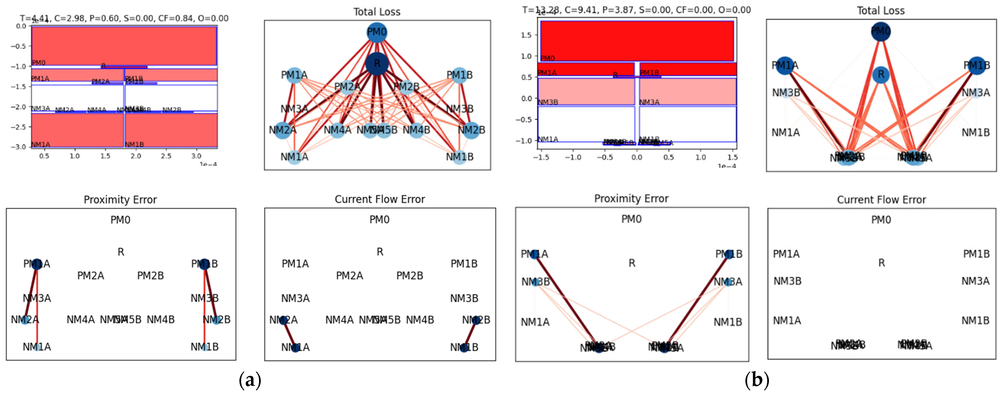
Figure 1. High-level synthesis flow of the proposed toolbox based on advanced DL techniques.
Electronics 11 03964 g001
Figure 2. ANN architecture that is used to solve the map from the physical dimensions and topological constraints to the placement coordinates.
Electronics 11 03964 g002
Figure 3. GUI: (a) Placement inspection, selection, interface; (b) Placement analysis and fine-tuning interface. Total error shown.
Electronics 11 03964 g003
Figure 4. Placements generated by Virtuoso XL, a human designer and the proposed toolbox, along with the total, the proximity and the current-flow error graphs. (a) Cadence generated placement. (b) Human designed placement. (c) Toolbox’s generated placement.
Electronics 11 03964 g004
Figure 5. Generated placements, instantiated in Cadence. From left to right, generated by: the proposed toolbox, Virtuoso XL and expert designer.
Electronics 11 03964 g005
Figure 6. Schematic of the LPLNA introduced in [26].
Electronics 11 03964 g006
Figure 7. Placements generated by a human designer and the proposed toolbox for the LPLNA [26], along with the total, the proximity, and the current-flow error graphs. (a) Human designed placement. (b) Toolbox’s generated placement.
Electronics 11 03964 g007
Table 1. Floorplans’ error comparison for the current starving single-stage amplifier biased by voltage-combiners.
PlacementCompactnessComp.ProximityComp.Current-FlowTotal ErrorComp.
Virtuoso XL24.773.99×19.426.37×0.0044.194.47×
Human [23]6.721.08×8.332.73×0.8915.941.61×
This Work6.21-3.05-0.629.89-
Table 2. Floorplans’ error comparison for the low-power, low-noise amplifier.
PlacementCompactnessComp.ProximityComp.Current-FlowTotal ErrorComp.
Human [26]2.98-0.6-0.844.41
This Work9.413.16×3.876.45×0.0013.283.01×
Publisher’s Note: MDPI stays neutral with regard to jurisdictional claims in published maps and institutional affiliations.

