1. Introduction
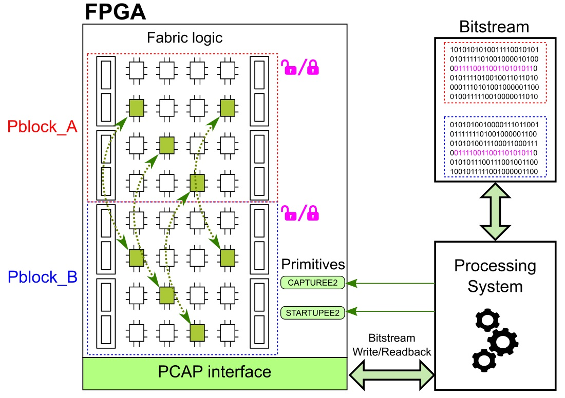
The increase in the integration level of electronic devices has boosted the use of SoC (System-on-Chip) designs. Due to their flexibility and continuous innovation, FPGAs (Field Programmable Gate Arrays) are one of the most interesting platforms for implementing these designs. FPGAs consist of arrays of configurable logic blocks that can be configured by the user to perform a custom functionality. In the case of certain FPGAs, such as SRAM-FPGAs, this configuration can partially run (a concept known as dynamic partial reconfiguration), increasing their functional capabilities and decreasing resource usage.
A tendency that is gaining momentum consists of coupling FPGA logic with built-in processor systems in a single device, making them even more attractive for SoC designers. A remarkable example in this regard is the ZYNQ from Xilinx, which consists of two main parts: a processing system with a dual ARM9 hardcore processor and a 7 series programmable logic fabric. A notable aspect of this architecture is the inclusion of a direct and customizable connection between the processing system and the FPGA fabric, providing higher adaptability, communication speed and performance. Due to those reasons, this research has been based on the ZYNQ technology.
A key element in most digital electronic designs is memories, as they are used to store different data types, such as program code, user data, variables, etc. In the case of FPGAs, there are two main ways to implement memory elements [
1]: by utilizing distributed general-purpose fabric logic or making use of dedicated BRAM (Block RAM) modules. Memories based on distributed general-purpose fabric logic are mainly utilized to implement reduced memory structures with fast access. This is because, due to the hardware overhead and the delay paths introduced when implementing large memories, these structures are not advisable for implementing big memory modules. On the other hand, BRAMs are commonly used to store a large amount of data. The reason for this is that, although BRAMs can also be utilized to implement small memories, the drawback, in this case, could be slow memory access and misuse of resources. Hence, depending on the requirements, the designer has to adopt an adequate solution, which usually includes a combination of both alternatives.
The standard way to access data in memories is based on utilizing dedicated input/output ports. However, this action presents certain limitations, such as the need for memory controllers, bus interfaces or auxiliary memories and limiting memory access during its use. An alternative to this is the use of the FPGA’s bitstream [
2]. The bitstream is a file whose content is stored in the configuration memory. This content involves the device’s configuration parameters, such as the resources used and their interconnection, initialization values and configuration options. It also includes (or can include) the initial data content of both BRAM and distributed memories. Nevertheless, working with the bitstream can be a tedious task because of the limited information about the bitstream structure released by vendors. In that sense, as [
3] describes, several studies have carried out reverse engineering strategies to increase the knowledge about the bitstream.
The main contribution of this work consists of utilizing bitstream to manage memory content. This approach provides benefits that could improve existing designs and enables new paths for several applications, such as data management, fault tolerance or security [
4,
5]. For instance, in the case of memories implemented as ROMs (widely utilized as program memories in soft-core processors), this approach offers an alternative way to carry out several applications, such as detecting errors by comparing the content of different instances of memories implemented in a hardware redundancy fault tolerance scheme, updating/repairing the program and data memories of soft-core processors, synchronizing the context in a processor redundancy system [
6], etc. Another specific example that makes an interesting approach based on utilizing the bitstream is the case of a faulty interface of a memory resource, for instance, damaged by an induced fault [
7]. If this occurs, the error can disable or affect significant ports, provoking permanent malfunction in the memory, which can be critical if the memory contains relevant information (especially if it has not been hardened). A bitstream-based approach can provide a solution in such unlikely but possible scenarios. In all those cases, and many other possible applications, one of the key advantages of this kind of approach is the reduction of hardware overhead, which usually implies lower power consumption, less logic susceptible to induced faults and higher availability and reliability.
Nevertheless, its main drawback is the time demand related to the reconfiguration process. In addition, managing data via the bitstream for BRAM or distributed memories requires specific methodologies and is a platform-dependent strategy. While the data management for BRAM memories of the Xilinx 7 series was addressed in [
8], a scarcity of investigations around distributed memories in such technology has been detected.
Bearing in mind the potential benefits that can be obtained with this strategy, this work proposes a novel methodology to manage the data content of distributed memories by utilizing the bitstream. This proposed methodology includes two design flows that enable this management to be carried out in a straightforward fashion. While the first design flow permits the protection or unprotection of partial reconfigurable regions against overwriting in order to be able to choose which regions are to be affected by the restore signal, the second flow provides an easy way to generate homogeneous implementations of a design in different reconfigurable regions, making the data processing much simpler.
The remainder of this document is structured as follows.
Section 2 surveys the existing approaches related to the management of distributed memory through the bitstream. Next,
Section 3 introduces the proposed methodology in detail, including the two proposed design flows. Validations and practical results are presented in
Section 4, and finally,
Section 5 outlines the conclusions and future work.
2. Existing Approaches
Managing user data content through the bitstream is a technology-dependent procedure that requires a deep knowledge of the structure of both the bitstream and the target FPGA device. While devices from the 7 series from Xilinx share the majority of the characteristics of the bitstream structure, there are differences with previous model families. Despite the fact that, in several cases, the flows and the main ideas can be adapted to different devices, the developed approaches are commonly related to a particular FPGA vendor, a particular FPGA series or even to a particular device. The lines below present the most significant works that deal with data management through the bitstream, focusing on the data content of distributed memories of Xilinx devices.
Jbits [
9] is one of the first tools reported to be able to modify the bitstream, including the data content. It consists of a set of Java classes that provides an application program interface into the configuration bitstream for XC4000 and Virtex families from Xilinx, and it does not require additional hardware structures. Nevertheless, it has limited efficiency since it needs to read the entire bitstream, while the user data only uses a relatively small percentage of it. This tool became obsolete, and it is not suitable for 7 series devices. Similarly, in [
10], the extraction and reconstruction of the status bits from the bitstream were successfully achieved for the same device. Although the proposed method was an interesting advance at the time, it is not applicable to modern devices either. Ref. [
11] is another example of obtaining information through the bitstream of older Xilinx devices. However, this method of extracting target information only functions for look-up tables (LUTs).
In [
12], a step forward toward bitstream-based data management was presented. This approach focuses on saving and relocating the context of a soft-core processor by extracting (and writing back once processed) the bitstream through the SelectMAP interface. In this process, the entire configuration data are not read back, but only the frames that contain the target information. In [
13], a similar approach proposing a partial displacement defragmentation algorithm for heterogeneous reconfigurable systems was presented. However, these approaches are limited to one-dimensional partial reconfiguration of FPGA families from Xilinx. Hence, they cannot be utilized in the newest devices. In addition, they require high processing effort and the use of tools, such as a configuration manager, the
PARTBIT software and the
REPLICA filter, to manage a complex database to store the placement of each data bit.
Later works, which tackle newer Xilinx devices, provide support for the case of two-dimensional partial reconfiguration. The approach presented in [
14] develops the capacity of capturing, storing and copying the content of flip-flops within a Virtex-V FPGA device on a particular reconfigurable region by utilizing the bitstream in combination with the
STARTUP_VIRTEX5 primitive, the
RECAPTURE commands and the ICAP interface. The ICAP interface is a point-to-point connection between the ICAP (Internal Configuration Access Port) primitive and the SEM (Soft Error Mitigation) Controller. In a further approach [
15], this approach was extended to enable copying the content of flip-flops between heterogeneous reconfigurable regions by processing the captured bitstreams. To determine which reconfigurable region is about to be targeted, both works follow the strategy depicted in
Figure 1 to protect/unprotect against overwriting. Since the entire FPGA design is unprotected (open padlocks) by default, in the first step, the entire FPGA design has to be protected. When the context needs to be saved, the target region has to be protected (closed padlock) before capturing the data. This protection is carried out by including specific commands in the partial bitstream. After capturing the data, the target region can optionally be protected. In any case, before restoring the context, the target region has to be unprotected. After finishing context saving/restoring processes, the target region can be protected in order to avoid undesired changes in future startup sequences. In [
16], the same authors presented an implementation of preemptive hardware multitasking for partially reconfigurable FPGAs that enables configuration prefetching and reuse. This approach, based on their previous works, reduces configuration overheads, improving the system performance.
In general, these first developed approaches to manage the registers’ content via bitstream present some common drawbacks. First, they are not suitable for modern devices because they are architecture-dependent. In addition, they require complex external controller devices and memories, and they provide low availability due to the time demand of the reconfiguration. Another limitation of these approaches is that they require the CRC (Cyclic Redundancy Check) feature of the generated bitstream to be disabled. Hence, the utilization of the CRC feature would require the generation of a new CRC value, which requires high processing effort [
17].
Regarding the bitstream manipulation of newer devices, such as the 7 series from Xilinx, some studies, such as [
18,
19], have been published. Nevertheless, these approaches target the logic structure of the device without focusing on the registers’ content. More recent works provide high-level design tools that enable bitstream manipulation to manage user data content in a more precise manner. For instance, Ref. [
20] is a remarkable tool that enables data of LUTs, CLBs and BRAMs to be managed through the bitstream. It also offers flexibility since it can be used as a standalone solution (running a Linux-based application in the ARM of the ZYNQ) or in Windows machines. However, since this is a high-level approach with complex software processing, it is a time-consuming solution (in the range of seconds). Although [
21] is another newer interesting example, in this case, only the BRAM content has been targeted.
Table 1 summarizes the presented approaches. In order to target the detected gap, the work presented in this manuscript proposes a low-level standalone alternative, which consists of different design flows, that allows registers’ content management to be performed through the bitstream in an autonomous way and a straightforward fashion. Although this methodology is based on the ZYNQ device, it is adaptable to other 7 series devices from Xilinx, with which it shares resources and bitstream features.
3. Description of the Proposed Approach
Since the developed methodology to access and manage data content of distributed memory via bitstream is based on 7 series devices from Xilinx, studying several relevant aspects related to flip-flops and flip-flop/latches (that can be configured as either flip-flops or latches) is required. For this reason, the most remarkable details are summarized in the following lines.
Each flip-flop of 7 series devices provides
SRHIGH/SRLOW (SRVAL) and
INIT0/INIT1 (INIT) options [
22]. Determined by the HDL (Hardware Description Language) design, each option and its value is configured and stored in the bitstream. The example from
Figure 2 shows a VHDL (VHSIC Hardware Description Language) code for a flip-flop where both INIT and SRVAL values can be determined. While SRVAL values are controlled by the local
SR control signal, INIT values are mainly utilized during the initialization after reconfiguration. However, INIT values can be updated by performing a context capture.
The
CAPTUREE2 primitive [
23] is a key tool from Xilinx for 7 series devices, which offers the possibility of capturing the state of user registers and storing it in the configuration memory by loading the
GCAPTURE command. An alternative to the utilization of the
CAPTUREE2 primitive is to load the
GCAPTURE command in the CMD (command) register of the bitstream. Thanks to this, current register (flip-flop and latch) values can be stored in the configuration memory by triggering the
CAP input from this primitive. These register values are stored in the same configuration memory cell that programs the init state configuration of registers (INIT values). These register values can be read from the device along with all other configuration memory contents by using the readback function. To take advantage of the
CAPTUREE2 primitive, it is necessary to previously know the location of each data bit in the bitstream. The most straightforward way to obtain this information is to use Xilinx’s software (Vivado, ISE, etc.) to generate the logic location text file (*.ll).
STARTUPE2 is the other key primitive that features an interface that relates the user logic resources with the status signal and the configuration logic control. This primitive can be utilized in an implementation to obtain user control over certain selected configuration signals during the operation. A relevant port of this primitive is the GSR (Global Set/Reset). The GSR resets the device by driving the GRESTORE command. This active high-input port leads an asynchronous set/reset signal that enables CLB/IO flip-flops and DSP (Digital Signal Processor) registers of the entire device in their initial state to be initialized. The initialization values of flip-flops are determined by the INIT0/INIT1 options defined in the bitstream. Furthermore, INIT values can be updated with actual values of registers via the GCAPTURE command. A remarkable aspect of the utilization of the GSR signal is that it does not require general-purpose routing. Considering that the skew and release processes are performed asynchronously, some flip-flops may be released in different clock cycles, causing metastable events. For this reason, it is advisable to stop the clock before asserting the GSR signal, to wait until it spreads across the entire device and to tightly cluster all the registers in order to minimize the path length.
The developed approach to managing data content via bitstream follows these presented ideas. First, both GCAPTURE and STARTUPE2 primitives have to be included in the design. Then, the functionality of both primitives can be controlled by the processing system of the ZYNQ via the EMIO interface. After the target design has been developed, the partial bitstreams of the reconfigurable modules to be managed have to be generated, enabling the .ll location file option (and, depending on the case, also the RESET_AFTER_RECONFIG=TRUE property). Then, the generated partial bitstreams and the .ll file have to be analyzed together (for example, with a .HEX editor) in order to determine the location of the target data bits. With the obtained data, an application to be used by the processing system has to be programmed, enabling the management of the data content bits. Since the functionality of the application depends on the target design, it has to be specifically programmed to fit the specifications needed. This application will use the PCAP (Processor Configuration Access Port) interface to read back the bitstream with the content of the source registers and download the modified bitstream with the content for the target registers. The developed application will be able to: control the GCAPTURE command to copy the data content of the registers in the partial bitstream, process the data and generate new partial bitstreams with the specific data content, download the generated partial bitstreams and control the GRESTORE command to load the data content stored in the partial bitstream to the device.
The proposed methodology includes two key flows to extend its functionality and to provide a straightforward and standalone data management process. While the first deals with the protection/unprotection against overwriting partial regions in 7 series, the second allows the generation of homogeneous implementations of a design in different reconfigurable regions in a straightforward fashion and without affecting efficiency. Both flows are discussed in the following lines.
3.1. Flow to Protect/Unprotect Partial Regions against Overwriting
A limitation of the CAPTUREE2 primitive is that it stores the content of the entire device in the configuration memory, even when only registers of certain reconfigurable areas are intended to be captured. Hence, the information of the rest of the registers, which should remain unchanged, would also be updated. To solve this problem, the resources of the reconfigurable region that must remain unchanged have to be protected by setting certain bits of the bitstream. This process requires a complex bitstream modification process that demands the knowledge of the location of certain specific command words. To overcome those issues, this work proposes a design flow that allows the protection or unprotection of the desired reconfigurable regions by performing straightforward modifications of partial bitstreams.
In [
14,
15], a method that carried out the protection/unprotection of Virtex-V devices was introduced. However, this method is not valid for the newer 7 series devices because, unlike Virtex-V devices, Xilinx has not released any information about protection/unprotection bits of the 7 series.
The only alternative available to the existing methods is to capture and restore the content of all the registers in the device. Thus, when to read/write data from/to particular areas is needed, as
Figure 3 depicts, context saving and restoring requires a relatively tedious process. First, the state of all registers has to be captured. In an initial state, the bitstream contains the INIT values predefined in the VHDL. In the case of triggering the capture signal without protecting any region, the content of all flip-flops is stored in specific locations of the bitstream. Hence, the data of the target region has to be extracted from the entire bitstream and saved in an external memory, which requires using and processing the information from the previously generated logic location text file (*.ll). To avoid overwriting the current value of the rest of flip-flops, it is necessary to capture their context and merge it with the previously stored one. Then, the created partial bitstream can be downloaded to the FPGA updating the content of the flip-flops memory loaded by triggering the
GSR signal. This method is a complex and time-demanding process since it requires several operations in each context saving/restoring action. In addition, it requires external memory and complex customized software for processing the bitstream.
To circumvent this problem, a novel design flow that enables the unprotection of as many reconfigurable regions as desired, keeping the rest of the design protected, is proposed. It also avoids the need to save data from other non-protected regions. Inspired by an idea suggested in [
16], the developed method enables the reading and writing of registers’ data of a particular region without affecting the rest of the device thanks to the
RESET_AFTER_RECONFIG=TRUE [
24] property. This can be used with 7 series devices to implement partially reconfigurable modules in order to avoid manual unprotection/protection actions. When implementing partially reconfigurable designs with this property in 7 series (for UltraScale devices is always enabled), the partial bitstream created by Vivado contains the commands to protect the rest of the device (including the static and the rest of the partial regions), keeping the actual partial region unprotected. Hence, this property enables protecting a particular partial region in a simpler manner. Nevertheless, as
Figure 4 shows, this method can only unprotect (open padlock) a single partial region at once. As it can be observed, every downloaded partial bitstream unprotects the reconfigurable target module and protects (closed padlock) the rest of the device, even if the partial reconfigurable module has been previously unprotected. Thus, there is no way to unprotect more than one partial region from the same device.
With the aim of solving the issue of unprotecting more than a single partial region in 7 series devices, a novel design flow has been developed in this work. As a first step, two reconfigurable regions (PblockA and PblockB) have been implemented. In this process, PblockA has been implemented by applying the RESET_AFTER_RECONFIG property, while PblockB has been implemented without this option. After that, both generated partial bitstreams were analyzed. For this task, a .HEX file editor has been utilized thoroughly, comparing the content (data words in hexadecimal notation) of both partial bitstreams. This comparison has shown remarkable differences in the content of both bitstreams, making it difficult to identify special bits or command words utilized to perform the protection/unprotection of the reconfigurable region. However, after further analysis and several tests performed by loading modified partial bitstreams and checking the result in the implemented hardware, a special word in the 51st position of the frame with a particular content (0xE00009BC) has been observed through the partial bitstream. Afterward, a new comparison was performed to detect discrepancies in the 0xE00009BC special word. The comparison results indicate that only two 0xE00009BC words appear in partial bitstream A and do not appear in partial bitstream B. Hence, it has been initially assumed that these two words were the protection words for reconfigurable region B. In this way, different tests have been carried out by modifying the partial bitstream of PblockA, downloading it and performing physical tests. After testing two distinct implementations per clock region and column of registers (28 in total) of the Zynq device, it has been concluded that erasing one of both special words has an effective protecting/unprotecting effect on the partial bitstreams.
Using this information, the flow described in
Figure 5 has been developed. It uses the
RESET_AFTER_RECONFIG=TRUE property in combination with the edition of the partial bitstream as a straightforward method to protect or unprotect as many partially reconfigurable modules as desired. Despite the fact that this flow can be used for several reconfigurable blocks, for the sake of simplicity, only two blocks (PblockA and PblockB) are targeted in this case. As described in
Figure 5, the flow consists of four steps:
A design that includes the two reconfigurable regions (PblockA and PblockB) has to be implemented by generating the complete bitstream and the two partial bitstreams. One of the partial bitstreams (partial bitstream A in this example) has to be generated, including the RESET_AFTER_RECONFIG property.
Once both partial bitstreams have been generated, the one generated without the RESET_AFTER_RECONFIG property (partial bitstream B in this case) has to be edited by erasing the proper 0xE00009BC word and stored.
Download the complete bitstream to the device.
The newly created partial bitstream has to be loaded to protect/unprotect the desired partial regions.
Once the partial regions have been unprotected, the content of the registers of the unprotected regions can be easily read and written by means of the GCAPTURE and the GRESTORE, respectively, without affecting the protected regions. When using the RESET _AFTER_RECONFIG property, it is advisable to use the SNAPPING_MODE constraint to automatically create legal reconfigurable blocks. This method, combined with bitstream processing, enables the altering of register data, i.e., copying data content from one register to another.
The main benefit of this method is its high speed, especially when capturing and restoring the context because both GCAPTURE and GRESTORE operations are not time-consuming processes. Thus, the time requirements are related to the time needed by the GSR signal to spread across the partially reconfigurable circuit, which is design-dependent. In addition, this approach enables both capturing and restoring of the context without the need of additional elements of external memories or logical resources to be performed.
A drawback of this approach is the need to implement partially reconfigurable blocks. When using the RESET_AFTER_RECONFIG=TRUE property, the partially reconfigurable module’s height must align to clock region boundaries, which means occupying an entire column of resources (there is no block width restriction). Further, if the XADC component is used, its interface access will be blocked during the partial reconfiguration. Another disadvantage of the use of the RESET_AFTER_RECONFIG=TRUE property is that, since the partial bitstream created contains the commands to protect the rest of the device and to unprotect the partial region, the size of the bitstream file increases.
Another potential limitation when using approaches that use partial reconfiguration is the reduction of the maximum achievable operating frequency of the design. Although two identical designs, one static and another reconfigurable, can be logically exactly equal from an RTL (Register-Transfer Level) description point of view, the way both are synthesized and implemented differs. The partial reconfiguration flow demands the synthesis of reconfigurable modules to guarantee that logical interfaces between static and reconfigurable partitions remain fixed. This limits cross-boundary optimizations. However, if the implementation is already designed as partially reconfigurable; this issue would not be relevant.
3.2. Location Constraint Flow: Generate Homogeneous Implementations of a Design in Different Reconfigurable Regions
When reading and writing user data from one memory block to another, two main cases can be found: homogeneous and heterogeneous implementations. While homogeneous designs share the main characteristics, such as size, shape and used resources (with equivalent fabric locations), heterogeneous modules support distinct features due to the usage of different resources, placements and granularity levels.
One of the biggest drawbacks of utilizing a bitstream-based strategy to manage the content of registers from one reconfigurable region to others is the required processing effort, which is significantly lower in the case of being homogeneous. This is because homogeneous designs require much simpler bitstream manipulations in order to relocate data. This aspect gains relevance in designs with a significant amount of registers, such as soft-core processors.
Even using the same HDL design for different reconfigurable blocks, due to the resource placement freedom of implementation tools, they create a heterogeneous implementation of each block. The simplest existing alternative to generate homogeneous implementations is to place all the resources of each instance manually in the same custom positions of each resource column utilized by the different reconfigurable regions. In designs with high resource usage, this task can be time demanding and require a high design effort. However, worse still is the fact that using this strategy requires deep design knowledge in order to obtain a proper implementation. Bearing in mind the advanced algorithms utilized by Vivado’s implementation tools, it is highly unlikely that a designer could obtain such an efficient implementation as Vivado.
In order to overcome those drawbacks, this section presents the developed design flow to obtain homogeneous implementations of a particular HDL design in distinct reconfigurable regions without affecting the optimized design generated by the synthesis software, which, for the sake of simplicity, will be referred to it as
Location Constraints Flow. This flow is based on utilizing the resource placement of one of the instances generated by Vivado to place the resources of the rest of the instances. Thanks to it, it is possible to obtain alike implementations in different regions for each design, placing each resource in the same positions of different columns (reconfigurable regions). A remarkable benefit of this approach is that it allows the copying process to be performed by copying entire bitstream portions and using a significantly simpler relocation process, and avoiding the need for data merging. Hence, it considerably simplifies the data copying program and minimizes performance penalties. This flow is specifically interesting in some designs that make use of hardware redundancy strategies, such as TMR (Triple Modular Redundancy) [
25,
26]. As described in
Figure 6, it consists of several steps:
Implement the previously synthesized design. This results in an implementation with the resource placement of each instance, making it possible to take advantage of the optimized implementation generated by Vivado.
Use the placement of one of the instances as a reference to generate new placements for the rest. This can be performed by using the write_xdc TCL command, which generates a .xdc file that specifies the cells utilized by each resource, providing a detailed list that contains the placement of all resources utilized by each instance.
Unplace all resources to avoid the possibility of relocating a resource to a location occupied by another resource from the original implementation. For this task, a script can be created using the unplace_cell TCL command combined with the information from the .xdc file.
Once the resources have been unplaced, they have to be placed again based on the locations of the reference instance following the same TCL script-based strategy. Nevertheless, in this case, it is necessary to specify the new locations to the place_cell command. This can be carried out in a straightforward fashion aided by a basic text editor by simply changing the number of columns (X coordinate) of each SLICE from the reference instance.
After placing the resources, the route_design and write_bitstream commands can be executed to obtain the complete and the partial bitstreams.
Download the design completed to the FPGA.
Thanks to the proposed Location Constraints Flow, an implementation with a proper placement can be obtained with minimal design costs, preserving the implementation tool’s efficiency and barely affecting performance when compared with an unconstrained design.
4. Experimental Setup and Physical Validation
An experimental setup has been designed for physical validation purposes, evaluating aspects, such as the impact on resource overhead, effects in terms of performance penalty, availability and functionality. A ZedBoard development board from AVNET, which includes a Xilinx Zynq-7000 AP SoC XC7Z020-CLG484 device, has been used for this task. The software utilized to develop and implement the different FPGA designs is Vivado Design Suite (2018.2).
The validation of the proposed flows has been performed through several tests. Many of these tests have been performed during the developing process of the technique. A simplified block diagram of the validation setup used for the design’s development and validation is shown in
Figure 7. Non-essential elements have been avoided to elude any possible impact on the bitstream’s content and structure. Initially, a very simple scheme has been designed by implementing two 8-bit registers in different reconfigurable areas. Reset ports of the two 8-bit register modules are managed by the processing system via the EMIO interface. The processing system also controls the
CAP and
GSR ports from
CAPTUREE2 and
STARTUPE2 primitives, respectively. With the aim of keeping simplicity and a faithful physical reading, the data input and output ports are connected directly to ZedBoard’s switches and LEDs (Light-Emitting Diodes), respectively. The switch connected to the first data bit also controls the multiplexer, providing the possibility of visualizing the connection between both registers in real-time. The bitstream is readback from the FPGA, combining the PCAP and the processing system, and stored in the DDR memory. The content of INIT values is obtained from the previously generated
.ll file. The identification of the location of the flip-flop’s content has been carried out by utilizing a text editor.
In the first validation step, the functionality of
GRESTORE and
GCAPTURE commands have been checked in a non-reconfigurable design with successful results. In addition, several data content copying experiments have been conducted with this setup. The basis of these tests has been a basic procedure: first, as
Figure 8 shows, specific placement constraints have been used in order to utilize the same flip-flops of different resource columns for both registers. As shown in
Figure 9, in which segments of .ll files are represented, it has been confirmed that the same structures (same frame offsets) are contained in the bitstream for the data of both registers, differing only in the FARs (Frame Address Registers). Utilizing this information, the content of one register has been copied to the other, with the bitstream confirming the viability of the proposed approach.
After, one of the registers has been implemented as a reconfigurable module enabling the RESET_AFTER_RECONFIG=TRUE property, keeping the other register and the rest of the design in the static region. In this case, the combination of the information extracted from read bitstreams, the .ll file and LEDs has proven that the utilization of the RESET_AFTER_RECONFIG=TRUE property protects the static area from the effect of the GCAPTURE command. In addition, it has been demonstrated that when generating bitstreams, the size of the bitstream considerably increases by enabling the RESET_AFTER_RECONFIG=TRUE property. In this example, in particular, it has been observed that while the size of a regular .bit file is 88.492 bytes, the size of a .bit file generated by the RESET_AFTER_RECONFIG=TRUE property is 240.108 bytes. As a consequence, an increase of 271.3% in the size of the bitstream has been detected. The main reason for this elevated percentage is that considering the small size of the partial bitstream, the instructions added to the bitstream to protect the reconfigurable region imply a significant data overhead. In larger reconfigurable designs, the impact of these instructions would be lower since the added instruction would represent a small data proportion of the entire bitstream. For instance, in a further test carried out with a larger design (the instance of the soft-core processor presented in the following validation), the increase in the size of the bitstream goes from 365.792 to 482.144 bytes, which implies an increase of 131.56%. Although this size increase in the bitstream usually does not suppose a remarkable drawback, in some cases, this is an aspect that could be relevant due to the effect of the size of the bitstream on the storage requirements and in the time necessary to program the device.
In a further step, the proposed Flow to Protect/Unprotect Partial Regions by editing the partial bitstream has been validated. In this case, both registers have been implemented in each reconfigurable Pblock. After editing one of the generated partial bitstreams by erasing the proper 0xE00009BC special words, it has been downloaded so as to reconfigure the FPGA. The information provided by the LEDs and bitstream readbacks in different GCAPTURE and GRESTORE tests have successfully demonstrated that both reconfigurable regions are unprotected while the static region remains protected.
Next, the
Location Constraints Flow has been validated. In this case, a TMR design with three instances of a PICDiY soft-core processor [
27] has been implemented in three reconfigurable regions (Pblock0, Pblock1 and Pblock2). In this first implementation, all resources of each instance have been freely placed by the tool. Thus, as can be observed in
Figure 10 obtained from the device diagram of Vivado, the three resultant implementations have presented distinct placements. Afterward, the
Location Constraints Flow was utilized to generate three alike implementations (selecting Pblock0 as a reference). As can be observed in
Figure 11, the resource placement of the three entities within three Pblocks has homogeneous architecture. In a similar way, the generated partial bitstreams of the three Pblocks have been compared in order to check if the location of data bits within the bitstream is the same. Furthermore, as
Table 2 and
Table 3 demonstrate, the resource usage of both implementations is almost the same.
Table 2 also confirms that the proposed design flow does not affect the implementation in terms of power consumption and maximum operation frequency. Further tests carried out on both implementations (with and without placement constraints) have demonstrated analogous results in terms of functionality.
In the final step, several registers’ content-copying tests between the different instances of the TMR design was carried out. After using the Location Constraints Flow, to obtain three equal instances of the processor and protecting/unprotecting the required reconfigurable regions, the processing system of the ZYNQ has been used by running a specific programmed application to copy the registers’ data content of one of the instances of the soft-core processor to the rest. The tests performed have proved that, thanks to the developed methodology, the data content of complex designs can be read, written and copied by using the bitstream, with a negligible effect, on both hardware overhead and performance penalty.
In addition, these tests have highlighted that the use of the bitstream to manage the data content of registers comes with the drawback of demanding a large amount of execution time. For example, in the case of copying data content from one of the instances of the soft-core processor to the other two, the process takes about 10 ms. The main reason for this time demand resides in the bitstream reading, manipulation and transferring processes. Hence, this time demand depends on the characteristics of each design, such as the number and type of implemented registers, their distribution, required data processing type, speed of the reconfiguration port, etc. In the presented example, considering the size of the bitstream, the amount of data to be processed is considerable. In addition, the program used to execute these processes utilizes general Xilinx functions, and it is not optimized for this specific application. For instance, the bitstream reading is performed frame by frame, and consequently, it affects the overall processing time of the proposed method. Therefore, the optimization of the functions to read more than one frame at once (i.e., bulk read) could make the technique faster. Another aspect that limits the speed of the approaches is the limited speed of the configuration port. An alternative in this direction could be exploring the capabilities provided by the reconfiguration controllers proposed in [
28,
29]. Thus, depending on several aspects, such as the size of the design, the location of resources, the processing power of the processor and the application executed, distinct timing results can be obtained. Hence, to obtain adequate results for particular designs, it is advisable to perform a specific timing analysis for each case.
5. Conclusions and Future Work
This work proposes a new straightforward and standalone approach to manage the data content of distributed memory by utilizing the bitstream for the ZYNQ device. This methodology includes two design flows that ease the designing process (one to protect/unprotect different partial regions and the other to obtain homogeneous instances of a design implemented in different reconfigurable regions). In this way, it enables the capturing or writing of the content of registers without significantly affecting the resource usage or design’s performance with simplicity and autonomy. By using the proposed method, the user data content of registers from different instances can be copied in a simpler and faster way compared with the few existing alternatives for 7 series devices from Xilinx. For instance, comparing it with the most remarkable one [
20], thanks to the low-level strategy adopted by the proposed approach, it requires fewer resources (a simple program based on Xilinx functions vs. a complete software tool running under linux OS) and time (seconds vs. milliseconds).
The developed approach provides useful features for several potential application fields, such as existing hardening techniques, data management applications, etc. Taking into account that 7 series devices from Xilinx are supported by Vivado software and share primitives, main features of logic resources and the bitstream structure [
22,
23,
30], the proposed methodology is likely to be easily adapted to devices from this family.
All the proposed approaches have been physically tested and validated on a ZYNQ device, proving their effectiveness. The performed tests proved the proper behavior of the protection/unprotection strategy. On the other hand, the tests performed with the Location Constraints Flow have shown that it enables exactly alike implementations of a design in different reconfigurable regions to be obtained without affecting the hardware overhead or the performance. In addition, the presented approach has been proven to be effective as a tool to copy the data content of registers of complex designs, such as TMR schemes of soft-core processors, through the bitstream.
There are some remarkable lines of research to give continuity to this work. For instance, this approach could be used to develop new applications or improve existing ones, such as checkpointing and rollback methods in lockstep implementations or the synchronization of repaired modules in TMR schemes [
31]. Another interesting approach could be to develop specific software to handle the bitstream in order to reduce the time demand of the data content-copying through the bitstream. In addition, the adaptation of the proposed strategies to different hardware platforms could be a very interesting approach. Since the proposed methodology has been closely developed for Xilinx 7 series device, an interesting research line could be to expand its use to other families, such as UltraScale from Xilinx, and even to other vendors’ devices, such as Intel (Altera), Microsemi, etc.


 ,
, 


