1. Introduction
In measuring small voltage deviations of about 1 µV and lower, it is important to separate a useful signal from noise. This problem is relevant to the metrological support of measuring transducers, such as inductive voltage dividers [
1,
2,
3,
4], current shunts [
5,
6,
7], current transformers, current clamps [
8,
9] for AC voltage measurements [
10,
11,
12,
13], vibration measurements of MEMS gyroscopes, accelerometers [
14,
15,
16] and other sensors [
17,
18,
19,
20,
21,
22,
23,
24]. The measurement of small voltage deviations between the amplitudes of two AC signals in wide frequency and voltage ranges is performed by using lock-in amplifiers with the differential input as a comparator (null-indicator and null-detector) [
25,
26].
The resolution and, consequently, measurement accuracy of lock-in amplifiers is largely determined by the common-mode rejection ratio (CMRR) in their measuring channel. The common-mode signal is the half-sum of voltages at measurement inputs of a lock-in amplifier. For example, if two 10 V voltages with 1 nV resolution are compared, the CMRR must be higher than 200 dB.
The best commercially available lock-in amplifiers [
27,
28,
29,
30,
31,
32,
33] demonstrate a 3–1 nV resolution, which is restricted by the CMRR of 100–120 dB, while its maximum input voltage is not over 1 or 3 V. This is insufficient, for example, metrological support of state-of-the-art measuring instruments, which requires to compare the root-mean-square (RMS) voltages of ≤10 V with a resolution to units of nanovolts.
For achievement in the real resolution range of 1–10 nV in the lock-in amplifier with voltages of over 1 V to be compared, it is necessary to achieve a result of transformations fully or partially independent from the common-mode signal, i.e., to implement a quasi-invariant common-mode signal.
This work presents the developed differential signal recovery circuit with embedded photovoltaic modules, which allows implementing the dual phase lock-in amplifier with the differential input and quasi-invariant common-mode signal. The structure of the paper includes three main sections: about lock-in amplifiers, our differential signal recovery circuit and our developed lock-in amplifier with increased CMRR.
2. Lock-In Amplifiers
Lock-in amplifiers are intended for a low-amplitude useful signal recovery from noise, whose amplitude is hundreds and thousands of times higher. With this purpose, the input signal is amplified and multiplied by a reference signal, the frequency of which equals the frequency of the useful signal. Next, the resulting signal is filtered from high frequencies [
34]. This approach is called synchronous demodulation or phase-sensitive detection. The reference signal is generated by the lock-in amplifier or an internal source. The phase-sensitive detection of the reference signal of the specified frequency provides a synchronous measurement on both fundamental and any harmonic frequency of the useful signal [
35,
36,
37,
38,
39,
40,
41,
42].
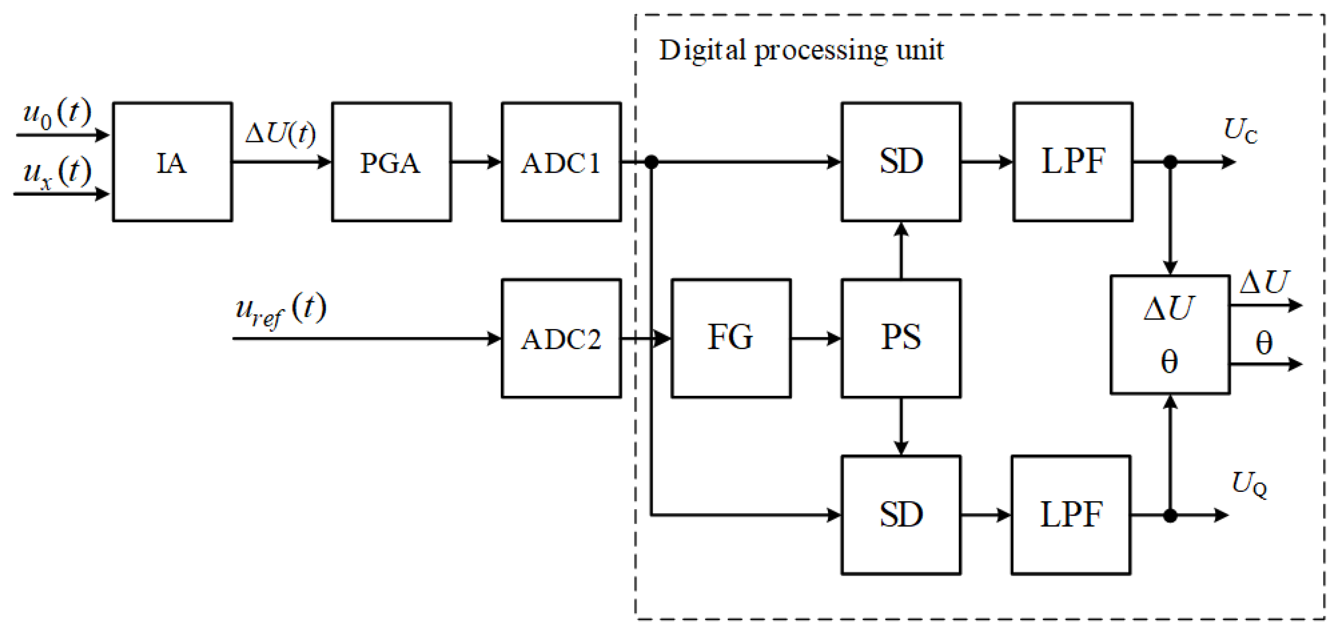
Figure 1 illustrates a typical flowchart of a commercially available lock-in amplifier [
27,
28,
29,
30,
31,
32,
33]. It consists of the instrumentation amplifier IA, programmable gain amplifier PGA, dual channel analog-to-digital converter ADC and digital processing unit.
Input voltages u0(t) and ux(t) are supplied to the IA. The differential voltage ΔU(t) is amplified by the PGA and processed by the ADC1. The reference voltage uref(t) is processed by the ADC2. The ADC output signals are processed in the digital processing unit. The latter implements the inner reference frequency generator FG, phase-shifter PS, synchronous detectors SD and low-frequency filters LFF. The signal processing provides the common-mode signal UC and quadrature signal UQ of the differential signal. Its module ΔU and phase θ are calculated in the same way.
Table 1 presents specifications for different models of commercially available lock-in amplifiers. Modern lock-in amplifiers are intended for the solutions of different problems, and this determines their high price and standard specifications. Being at the level of typical microcircuits of instrumentation amplifiers, the low common-mode rejection ratio (CMRR) is typical for all commercially available lock-in amplifiers, which makes it impossible to apply standard lock-in amplifiers for the recovery difference of two signals with a high resolution.
As can be seen from
Table 1, the real resolution of modern lock-in amplifiers is restricted by 100–120 dB CMRR of the input instrumentation amplifier, while their maximum input voltage does not exceed 1 V, which is insufficient for, for example, metrological support of state-of-the-art measuring instruments, which requires comparing RMS voltages of ≤10 V with a resolution in units of nanovolts.
The analysis of errors produced by the main units (see
Figure 1) given in our early research [
43] shows that the resolution of lock-in amplifiers is mostly affected by the common-mode signal of the input instrumentation amplifier. The development of solutions is, therefore, required to increase the CMRR and develop lock-in amplifiers with quasi-invariant common-mode signal.
3. Differential Signal Recovery
The circuit solutions based on the common-mode signal compensation, data correction of the common-mode signal and voltage follower can be used to increase the CMRR in IA subtraction circuits and to design lock-in amplifiers with a quasi-invariant common-mode signal.
The common-mode signal compensation and correction circuits have significant limitations [
44,
45,
46,
47] that restrict their practical use in lock-in amplifiers. These limitations include a limited maximum amplitude of input signals owing to a low IA voltage, at least two IAs with identical parameters, additional functional modules with super low-level errors of both the modulus and phase shift transfer factors in a wide frequency range.
The input range can be broadened without the voltage increase of the IA supply voltage, and the common-mode rejection ratio can be, thus, increased via changing the IA supply voltage in sync with changing the input common mode voltage [
48].
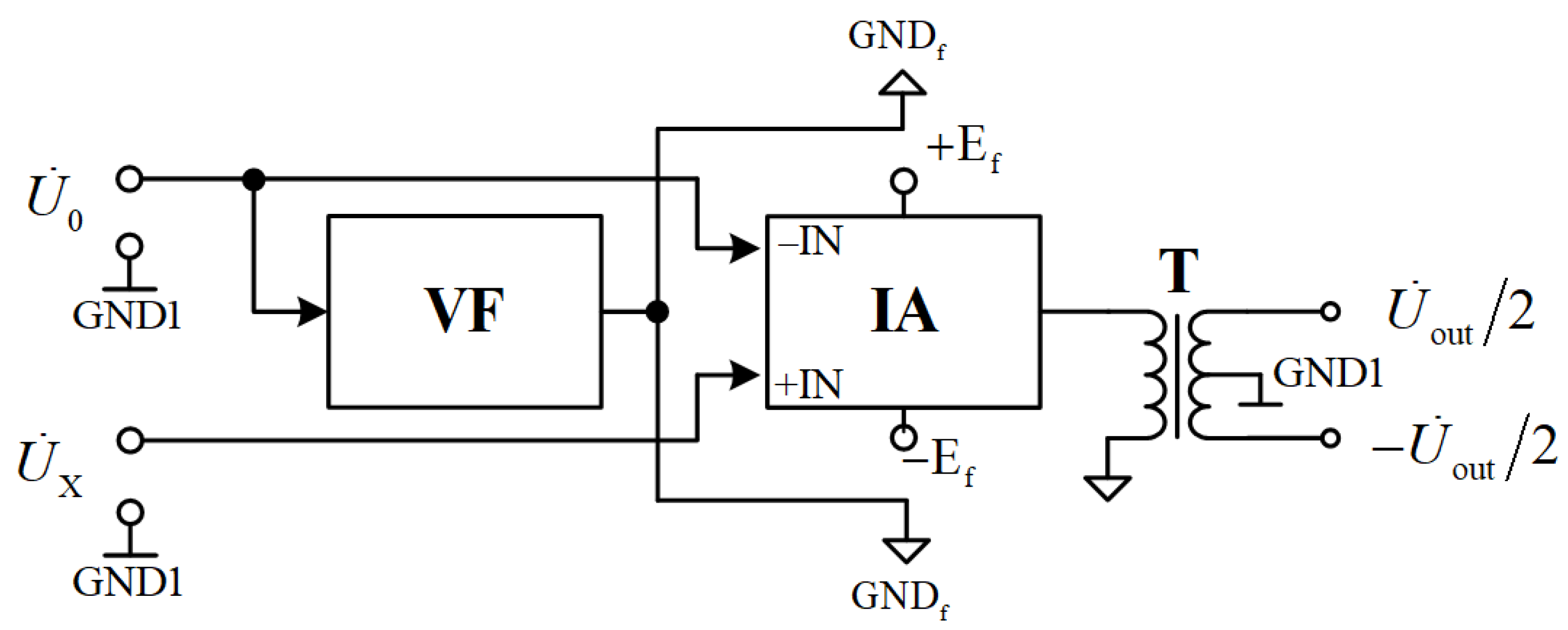
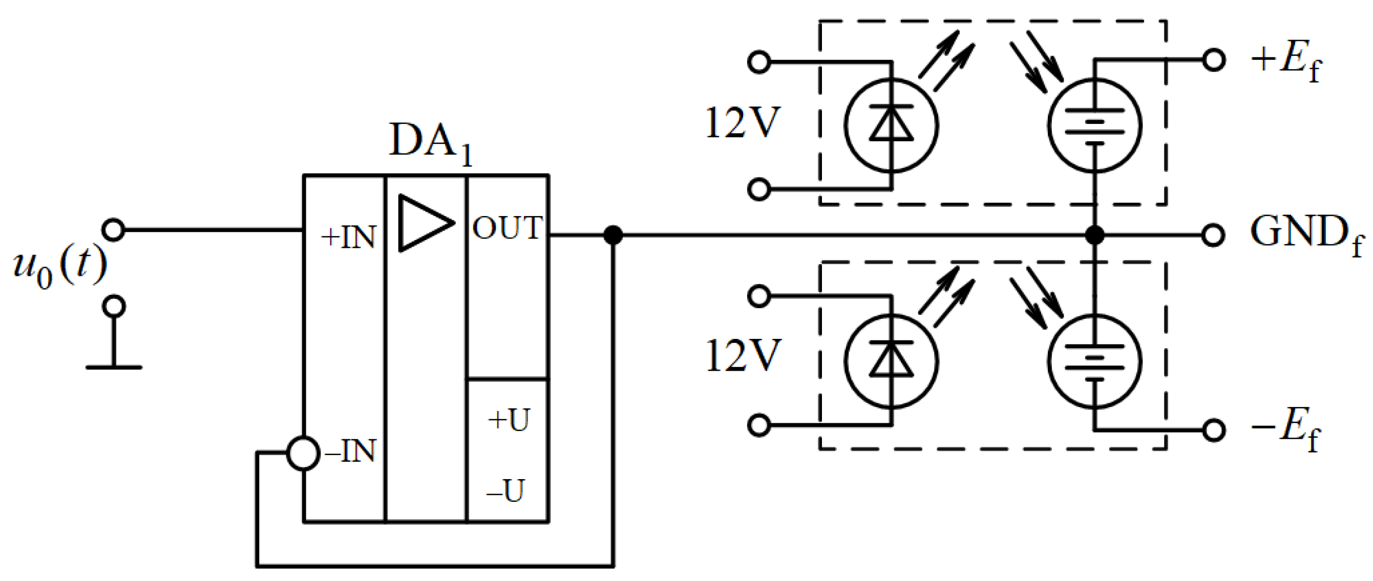
Figure 2 shows the schematic circuit of the differential signal recovery based on the voltage follower, which utilizes this principle for the CMRR increase.
The input voltages of the instrumentation amplifier can be written as
where
UX and
U0 are the voltages to be compared, V; and
Kf is the is the complex transfer factor of the voltage follower.
The output voltage of the instrumentation amplifier relative to the GND
f is as follows:
In the case of
UXcos(ω
t) =
U0cos(ω
t), the modulus and the voltage phase at the IA output with the voltage follower connection are determined by the following relations:
Therefore, the common-mode rejection ratio directly depends on the accuracy of the complex transfer factor of the voltage follower.
The voltage follower output stage with embedded photovoltaic modules is designed to implement the voltage follower circuit in practice (see
Figure 3). These photovoltaic modules are the solar cell array, which generates constant voltage when exposed to light.
The circuit simulation is performed in the NI Multisim simulation program based on an OP285 operating amplifier and photovoltaic modules with 5.6 V design output voltage and 1 W maximum power. Photovoltaic modules are connected to create constant symmetrical voltage ±Ef when exposed to the light-emitting diode array with the IA quasi-GND for the instrumental amplifier, which is formed by the voltage follower and named GNDf. The light-emitting diode array is supplied by a single constant voltage source E1, not connected galvanically to the voltage follower circuit.
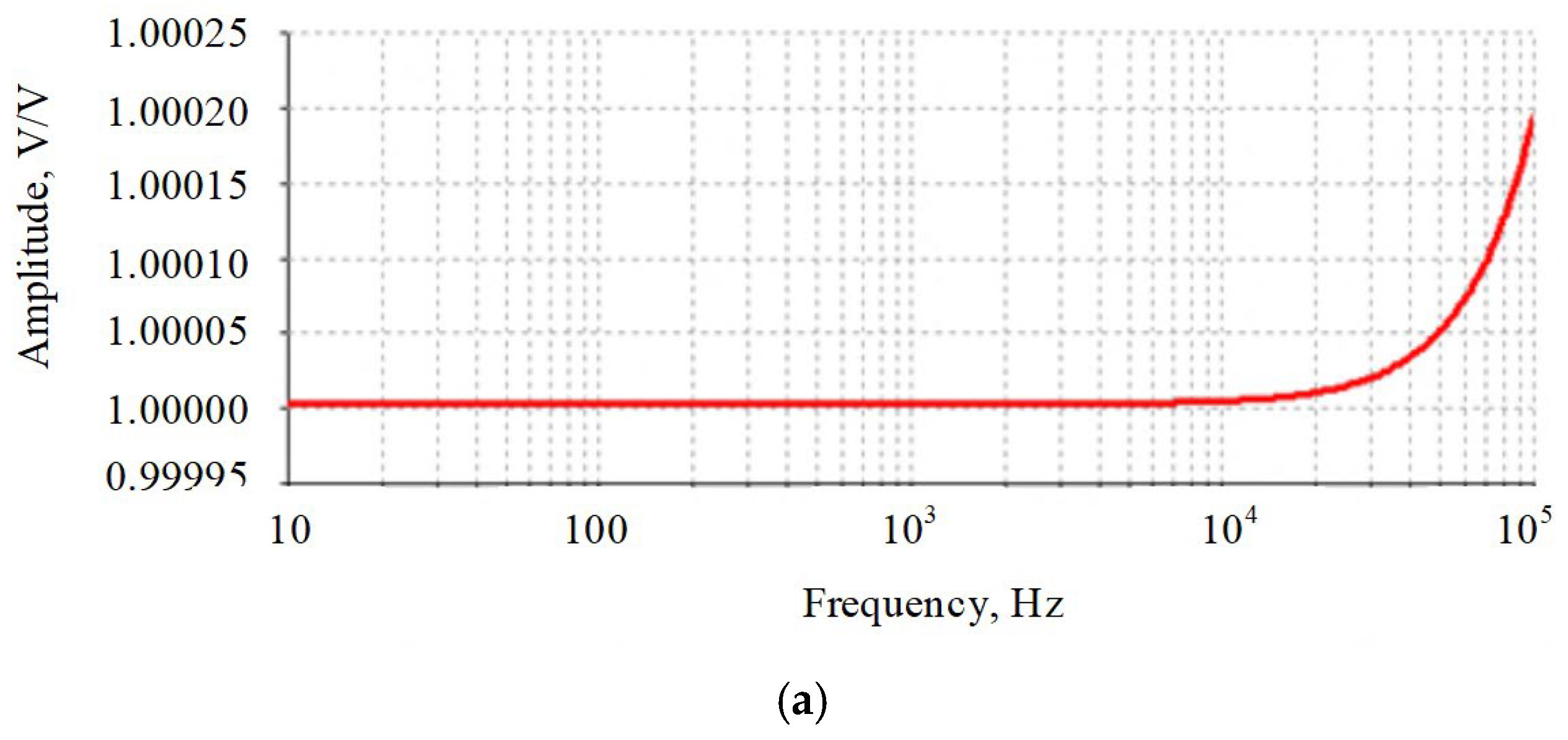
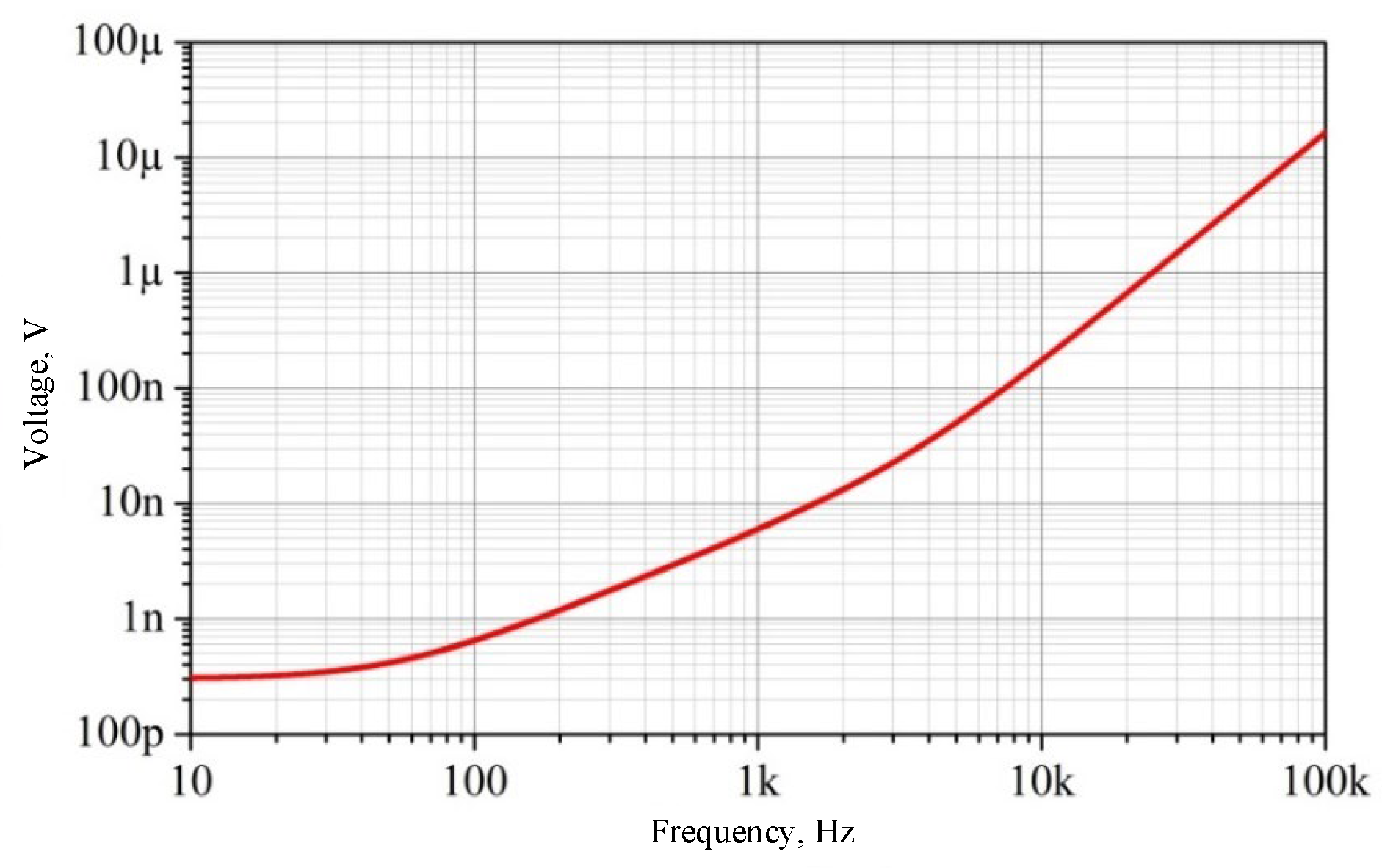
In
Figure 4, NI Multisim is used to simulate the amplitude frequency and phase-shift-frequency responses of the voltage follower output stage with embedded photovoltaic modules.
Based on (3) and the simulation of
UXcos(ω
t) =
U0cos(ω
t) common-mode signals with 10 V amplitude, we obtain the frequency dependence presented in
Figure 5 for the standard PGA207 instrumental amplifier with the design 100 dB CMRR and a 20 dB decrease per decade of ≈5 kHz [
48]. According to
Figure 5, the CMRR increases by 80 dB resulting in 180 dB on a 1 kHz frequency.
SunPower flexible monocrystalline solar cells C60 (Xuancheng, Anhui, China), a voltage follower based on OP285 operating amplifier and a PGA207 instrumental amplifier are used to assemble the prototype of the differential signal recovery as illustrated in
Figure 6.
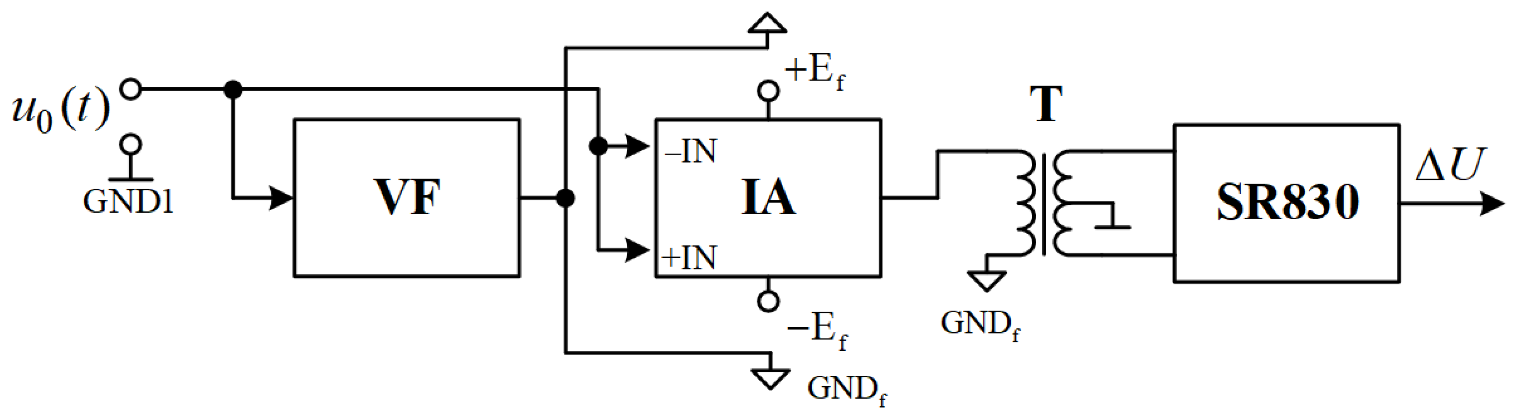
The CMRR is experimentally detected in the prototype of the differential signal recovery by using the circuit shown in
Figure 7.
Both inputs of the differential signal recovery are supplied by a Fluke 5520 calibrator with 1, 5 and 10 V sinusoidal voltage u0(t) on frequencies of 20, 40, 80 and 400 Hz and 1, 10, 20, 40, 80 and 100 kHz. The output voltage of the transformer is measured by an SR830 lock-in amplifier. The IA gain is 10, and the transfer factor of the transformer is 2.
The CMRR can be obtained from
where
UC is the input common mode voltage, V;
KIA is the IA gain; and
KT is the transfer factor of the transformer.
The experimental results are given in
Table 2.
As presented in
Table 2, the implemented circuit of the IA voltage follower output stage with embedded photovoltaic modules provides an 80 dB increase in the CMRR, i.e., up to 100–180 dB in the frequency range up to 100 kHz. This proves the achieved quasi-invariance to the common-mode signal in this frequency range.
4. Lock-In Amplifier with Increased CMRR
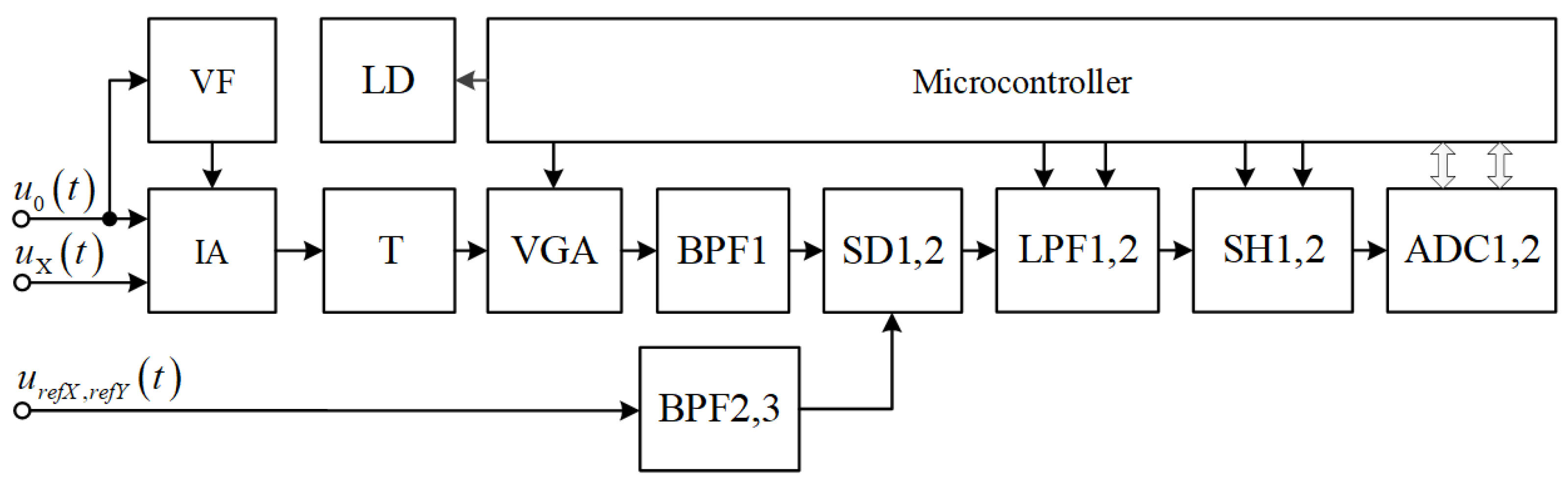
Based on the proposed signal recovery, we developed the dual phase lock-in amplifier with the differential input for checking the suggested circuit solution in a real device. The flowchart of the dual phase analog lock-in amplifier is presented in
Figure 8.
According to
Figure 8, the lock-in amplifier consists of the input IA with the voltage follower VF (see
Figure 2 and
Figure 3); isolating transformer T, which has one primary coil with 100 turns and two secondary coils with 100 turns each, with the common midpoint; the three-stage voltage amplifier VGA comprising three in-series IAs PGA207; the two-stage bandpass filters BPF1, BPF2 and BPF3. The first stage is a second-order Bessel high-pass filter with a 0.1 Hz cutoff frequency, and the second is a second-order Bessel low-pass filter with a 4 MHz cutoff frequency.
The filters are assembled in a OP285 operating amplifier. The lock-in amplifier also includes synchronous detectors SD1 and SD2 mounted to AD734 with the denomination factor close to unity; low-pass filters LPF1 and LPF2 are fabricated on the OP285 operating amplifier according to the third-order Bessel filter with a 0.1 Hz cutoff frequency; sample-and-hold circuits SH1 and SH2 made as described in [
49]; MAX110 analog-to-digital converters ADC1 and ADC2; a STM32F103 microcontroller; and indicator LD, which is a four-digit seven-segment LED module.
The comparable voltages are supplied to the IA differential inputs. The differential voltage Δu(t) at the IA output is supplied to the programmable three-stage voltage amplifier VGA via the isolating transformer T. The VGA output voltage is filtered by the two-stage bandpass filter BPF1. The BPF1 output voltage is supplied to the first inputs of the synchronous detectors SD1 and SD2. Reference in-phase and quadrature voltages are supplied to the second inputs of the SD1 and SD2 via two-stage bandpass filters BPF2 and BPF3. Voltages from SD1 and SD2 are filtered by low-pass filters and digitalized in analog-to-digital converters. The module and phase of the differential voltage are then calculated in a STM32F103 microcontroller. The resulting value is displayed by the indicator LD.
The flowchart of the dual phase analog lock-in amplifier implies the calibration of instrumentation channels. For this purpose, sample-and-hold circuits SH1 and SH2 are used. During calibration, both IA inputs are supplied by the standard voltage u0(t), sample-and-hold circuits being in a sample mode. Then, zero adjustment is performed through the SH transfer to the hold mode, and the indicator readouts are zeroed.
The microcontroller is also used to control the gain of the programmable amplifier, low-pass filters and sample-and-hold circuits operating modes. The external view of the PCB after mounting of the developed lock-in amplifier is presented in
Figure 9. The output voltage module of the lock-in amplifier can be obtained from
where
UC and
UQ are the in-phase and quadrature signals at the outputs of the LPF1 and LPF2, respectively;
KIA is the design gain 10 of the IA subtraction circuit;
KT is the transfer factor 2 of the isolating transformer T;
KVGA is the design gain of 1, 10, 100 and 1000 of the three-stage voltage amplifier VGA;
KLPF is the design gain of 1 and 10 of the low-pass filters; and
Uref is the reference voltage.
4.1. CMRR Estimation in Lock-In Amplifier
The CMRR of the lock-in amplifier was measured as follows. The signal generator OWON AG1022 was used to supply voltage
u0(
t) 5√2 V on 20, 40, 80 and 400 Hz and 1, 10, 20, 40, 80 and 100 kHz frequencies from the channel CHA to both inputs of the lock-in amplifier. The channel CHA output was connected to the in-phase reference signal input. From the channel CHB, the quadrature reference signal input was supplied by the voltage of the same amplitude and frequency but with a 90-degree phase shift. The output voltage Δ
U was measured, while the CMRR was calculated from
The resulting values of the CMRR with and without sample-and-hold circuits are summarized in
Table 3. As can be seen from
Table 3, the CMRR of the lock-in amplifier with the sample-and-hold circuit varies from 133 to 180 dB at a frequency of not over 100 kHz.
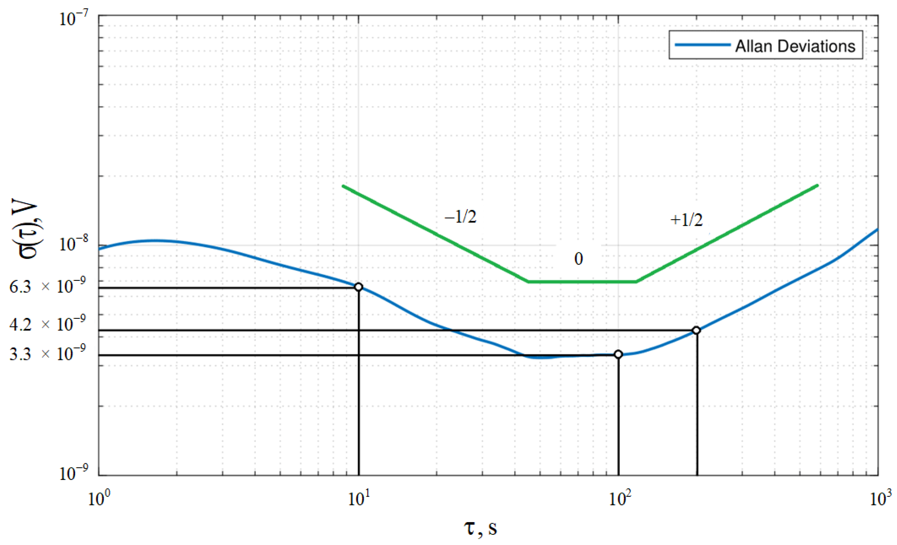
4.2. Noise Single Component
The measurement of the noise signal component of the lock-in amplifier was based on the Allan variance at the differential voltage of 1 µV at 1 kHz at the output of the inductive voltage divider DI-3m [
50]. The output voltage of the lock-in amplifier was measured for 1 h without using the sample-and-hold circuits. The number of measurements was 720,000.
Figure 10 presents the Allan variance of the lock-in amplifier on a logarithmic scale obtained after the output voltage measurements. A random walk of the output voltage is characterized by the white noise spectrum, and its coefficient is calculated by using the Allan variance at −1/2 inclination within the respective time range:
The white noise is, thus, 20 nV/√ Hz.
The flicker noise appeared during long-term measurements, which resulted from the electronic parts susceptible to random flickering. Due to its low frequency, the flicker noise was indicated as the data offset fluctuation. Knowing the Allan variance (at a zero inclination), its coefficient was determined as
and, thus, equal to 5 nV.
The random walk rate was described by the brown noise spectrum at the lock-in amplifier output, while its coefficient was calculated using the Allan variance at ½ inclination within the respective time range:
The brown noise is, thus, 0.5 nV·√ Hz.
The white noise level at the lock-in amplifier output was determined by multiplying the obtained value of the white noise by the square root of the transition band of the low-frequency filter:
The white noise level is 9 nV.
4.3. Resolution of Lock-In Amplifier
The resolution of the lock-in amplifier was measured in accordance with the circuit presented in
Figure 11.
The 1√2 V output voltage at 1 kHz was supplied from the channel CHA of the signal generator OWON AG1022. The same voltage was supplied from the channel CHB but with a 90-degree phase shift.
According to
Figure 11, at output
1, the transfer factor of the voltage divider DI-3 m [
50] was 0.500000, whereas at output
2, it varied from 0.500010 to 0.500050.
The relative deviation in measurements is calculated from
where
UDI is the differential voltage at the DI-3m outputs, V; and Δ
U is the output voltage of the lock-in amplifier, V.
At resolutions of 1 and 100 nV, the lock-in amplifier gain was determined as 2000 (
KLIA =
KIA·
KT·
KVGA·
KLPF = 10 × 2 × 100 × 1 = 2000). At a resolution of 10 nV, this factor was 20,000 (
KLIA =
KIA·
KT·
KVGA·
KLPF = 10 × 2 × 100 × 10 = 20,000). The resolution values obtained for the lock-in amplifier using the voltage follower output stage with embedded photovoltaic modules are given in
Table 4.
As can be seen from
Table 4, the relative error of the lock-in amplifier at a 10 and 100 nV resolution does not exceed 1.4% and 1.2%, respectively.
4.4. Frequency Range of Lock-In Amplifier
The estimation of the frequency range of compared voltages was performed by using the flowchart in
Figure 11. The output voltage 5√2 and 0.1√2 V at 1 kHz was supplied from the channel CHA of the signal generator OWON AG1022, and the same voltage was supplied from the CHB channel but with a 90-degree phase shift.
The transfer factor of the inductive voltage divider DI-3m was 0.100000 at output
1 and 0.100010 at output
2, i.e., the differential input voltage of the lock-in amplifier was 50 µV at 5√2 V from the signal generator OWON AG1022. The differential voltage was measured at 100 nV resolution on frequencies of 20, 40, 80 and 400 Hz and 1, 10, 20, 40, 80 and 100 kHz. The relative deviation in measurements at different frequencies is calculated from
where Δ
Uf=1 Hz is the output voltage of lock-in amplifier on 1 kHz frequency, V; Δ
Uf is the output voltage of lock-in amplifier on frequency different from 1 kHz.
The gain of the lock-in amplifier was 2000 and 20,000 for compared voltages of 0.5√2 and 0.01√2 V, respectively. The frequency values determined for the compared voltages using the flowchart given in
Figure 11 are presented in
Table 5.
According to this table, the relative deviation is not over 3.5% in the operating frequency range.
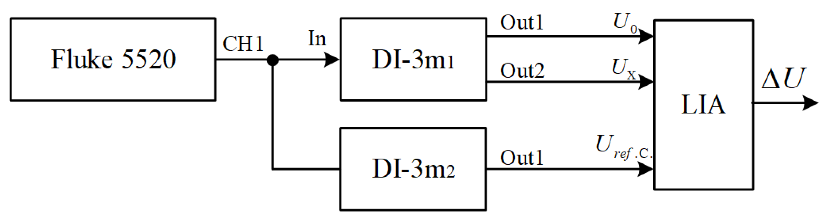
4.5. Minimum and Maximum Amplitudes of Voltages Compared
The estimation of the minimum amplitude of compared voltages was performed by using the flowchart in
Figure 11. The output voltage of 1√2 V at 1 kHz was supplied from the channel CHA of the signal generator OWON AG1022, and the same voltage but with a 90-degree phase shift was supplied from the CHB channel.
The transfer factor of the inductive voltage divider DI-3m was 0.000000 at output
1 and 0.000010 to 0.000050 at output
2, i.e., the differential voltage measured by the lock-in amplifier was varied from 10 to 50 µV. The minimum amplitude measurement of the compared voltage was conducted at a 100 nV resolution and 20,000 gain of the lock-in amplifier. The relative deviation in measurements was calculated by (11). The flowchart of the maximum amplitude of the compared voltages is given in
Figure 12.
The output voltage of 10√2 V and 1 kHz was supplied from the Fluke 5520 calibrator. The transfer factor of the first voltage divider DI-31 was 1.000000 at output 1 and 0.999999 at output 2. The transfer factor of the first voltage divider DI-31 at output 2 was changed from 0.999999 to 0.999995. The reference voltage was supplied from output 1 of the second voltage divider DI-32; the transfer factor was 0.500000.
The minimum and maximum amplitudes of the compared voltages are presented in
Table 6.
According to this table, the dynamic range RMS deviation of the compared voltages is not over 2.68%. This paper clearly shows that the definite metrological parameters of the proposed dual phase analog lock-in amplifier with differential input prove its applicability in comparing two signal amplitudes of 10√2 µV to 10√2 V in the frequency range of 20 Hz to 100 kHz with a 10 nV resolution and 180 dB common-mode signal.
Table 7 presents specifications for different models of commercially available lock-in amplifiers and our dual phase analog lock-in amplifier.
5. Conclusions
In this paper, we presented a developed differential signal recovery circuit with embedded photovoltaic modules and a dual phase lock-in amplifier with a differential input and quasi-invariant common-mode signal.
The embedded photovoltaic modules of the voltage follower in the signal recovery and the sample-and-hold circuit in the measurement channel of the lock-in amplifier allowed increasing the CMRR by 80 dB in the frequency range up to 100 kHz, which proved the gain in the quasi-invariant common-mode signal within that frequency range.
The proposed dual phase analog lock-in amplifier was characterized by a 130 to 185 dB CMRR in the frequency range up to 100 kHz, 20 nV/√Hz white noise calculated by the Allan variance, the resolution, the frequency range of the compared voltages and their dynamic range.
The obtained metrological parameters of the proposed dual phase analog lock-in amplifier proved their applicability in comparing two signal amplitudes of 10√2 µV to 10√2 V in the frequency range of 20 Hz to 100 kHz with a 10 nV resolution.
Future works should consider the substitution of analog synchronous detectors, bandpass filters, low-frequency filters and sample-and-hold circuits for their digital equivalents with the purpose to design a digital lock-in amplifier and further improve the metrological parameters based on digital signal processing.


