1. Introduction
Recent advances in artificial intelligence and big data have led to a growing demand for high-speed, energy-efficient computing. However, energy consumption and delay problems occur due to the frequent data transfer in the widely used Von Neumann architecture, known as the Von Neumann bottleneck or memory wall. In order to tackle this problem, the concept of in-memory computing has been introduced. Depending on how the memory is used for computing, the concept can be subdivided into smaller categories, including computation-near-memory [
1], which only shortens the distance between storage and the computation core, and logic-in-memory [
2,
3], which performs the computation inside the memory. Computing-in-memory (CIM) is also a major approach in in-memory computing [
4,
5]. In most designs, CIM performs the multiply-and-accumulate (MAC) operation using the memory array and its peripheral circuits through analog computing methods, greatly reducing the amount of data transfer required. SRAM-based in-memory computing [
6], with advantages in its technological maturity and high-speed read–write access, is a major topic in the CIM field [
7].
Computation in the charge domain [
8] is a common method for SRAM-based CIM, and is normally accomplished by pre-charging a capacitance on the bitline and then discharging it through wordline activation. The data stored inside the SRAM is known as the weight, whereas wordline activation represents the input data. In an SRAM-based CIM analog compute action, different amounts of electrons are discharged from a pre-charged bitline capacitance, representing the calculation result. In order to increase throughput (in other words, the amount of MAC operations done in a single round of computation), multi-row read operations need to be performed to accumulate multiple multiplication results in one round [
9]. However, many problems occur in such a process. Opening multiple rows simultaneously creates a large discharge current, requiring a bigger bitline capacitance, and resulting in greater power consumption. Moreover, the accumulation of several multiplication results widens the range of results, leading to more analog result levels, which demands a bigger output voltage swing for an easier analog-to-digital transfer process. Unfortunately, the analog results become nonlinear once the output swing widens. This is mainly caused by a change in discharge current related to the voltage of the bitline. To enable the continuous development of SRAM-based CIMs that use analog computing, these problems must be solved. Machine learning is a major application for CIM designs. Only when the precision of CIMs is improved can CIMs be used in circumstances that use complex algorithms and bigger data sets.
2. Recent Techniques
In order to tackle this challenge and resolve the problems above, researchers have used the following schemes: 1. Use only binary or ternary weights and inputs, cutting down on analog result levels and the amount of voltage discharged [
10]. 2. Off-chip methods, accounting the nonlinearity into the model and increasing the recognition rate through training, such as [
11], which happens under a deep neural network (DNN) circumstance. 3. On-chip circuit methods, as in the present work, to solve or minimize the effects. The first two schemes have the disadvantage of constraint to low-bit computation. Furthermore, they increase the amount of data transferred on- and off-chip, which contrasts with the fundamental targets of CIM, so on-chip solutions are fairly proposed. Related works that have used on-chip circuit methods are as follows: Z. Lin in [
12] proposed a current-mirror-based compensation circuit which provided an extra charge current for the bitline when the voltage is low. In [
13], they improved their design by separating the capacitance and the bitline with a cascade current mirror. A. Jaiswal in [
14] proposed the addition of operational amplifiers to the end of each 4 bit column in order to convert voltage results to linear current results. X. Si proposed to split multi-bit calculation into two rounds and shift-adding them together [
15]. S. K. Gonugondla in [
16] proposed a multiple switch and capacitance circuit to improve functional read performance. These designs share common deficiencies either in output swing or computation precision. This pressures the A/D module normally used to convert the analog compute result in a CIM design, so further study on the topic is needed.
3. Proposed Circuit
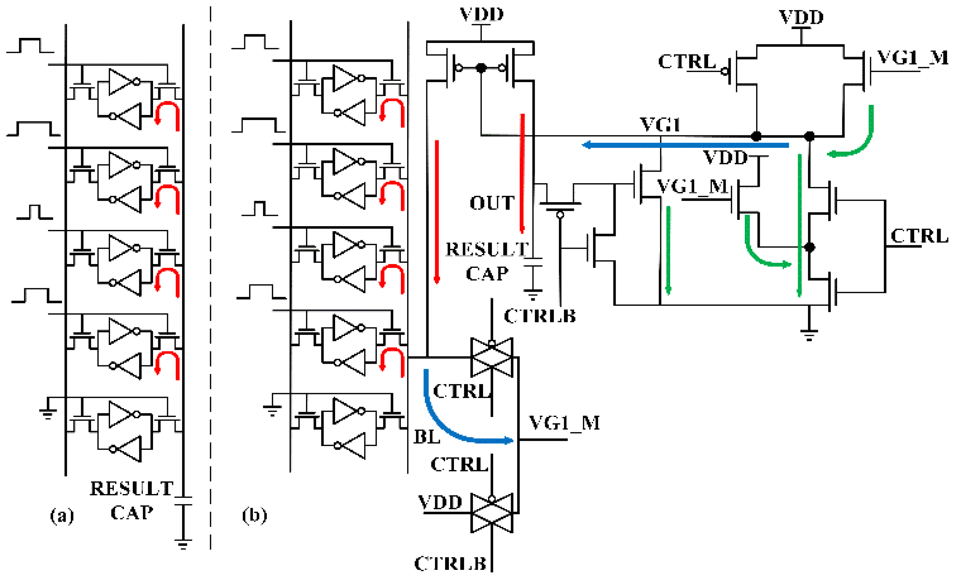
In order to achieve the goal of producing a precise and wide-swing output result for analog computation in CIM multi-row read operations, we propose a peripheral compensation circuit. The schematic of the proposed low computing leakage, wide-swing output compensation circuit is shown in
Figure 1. The compensation circuit is composed of a current mirror, a current competition circuit, and an additional pull-down circuit.
The current mirror provides a charge current for the bitline BL, which neutralizes the discharge currents of the SRAM cells during the CIM multi-row read operation and keeps the voltage of the bitline at a steady level, eliminating linearity problems caused by voltage decline on the bitline. Furthermore, it charges the result capacitor as the computing result, according to the discharge current created by the SRAM cells on the bitline. The output for the current mirror is decided by VG1, which indicates the change in the discharge current.
The current competition circuit acts as feedback for the bitline discharge current conditions in real time. This is achieved through NM1, NM2, NM3 and NM5. During the computing process, CTRL is set to high voltage and both NM1 and NM3 are at conduction state. On the other hand, NM2 and NM5 are controlled by the voltage of VG1_M, which is related to the voltage of the bitline. When the discharge current of the SRAM cells is large, the voltage of the bitline and VG1_M declines, meaning that less charge current flows past NM5 on to VG1. Furthermore, it causes a greater discharge current to flow past NM1 and NM3. Together, the voltage of VG1 is lowered, and more charge current is provided by the current mirror for the bitline and the result capacitor. On the contrary, when the voltage of the bitline is high, more charge current is provided by NM5 and less discharge current flows past NM1 and NM3. This is caused by the increase in current from NM2. This feedback helps to keep the voltage level of the bitline stable and creates a dynamic charge current for the result capacitor.
The additional pull-down circuit pulls down the voltage of VG1 even further through NM4 when the OUT voltage is high. This is crucial because a smaller gap between VDD and OUT causes the charge current to decrease, and therefore further compensation is needed for linearity.
The whole process of using the proposed compensation circuit in a CIM multi-row read operation is as follows: 1. First, in the preparation stage, CTRL is set to low and CTRLB is set to high. Consequently, both VG1_M and VG1 are pulled to high voltage, so the compensation circuit does not work in this stage. Additionally, the bitline is pre-charged to VDD and the result capacitor is reset to VSS in this phase. 2. The compute process of the CIM multi-row read operation starts, CTRL is set to high, and CTRLB is set to low. In this phase, the current competition circuit feeds back the bitline discharge current, and the current mirror provides charge current for the bitline and result capacitor. The additional pull-down circuit is activated if the result is large. 3. The compute process is not over yet, but all wordlines have already been deactivated. This is caused by possible small input and can be called the standby phase. The current compensation circuit minimizes possible computing leakage created by the current mirror in this stage, thereby preventing overcharge for the result capacitor. 4. The compute process ends, CTRL is set back to low, and CTRLB is set to high. The compensation circuit is deactivated, and results can be read by the following modules.
The multi-row read operation in conventional CIM designs is shown in
Figure 2a. The SRAM cells discharge from the pre-charged result capacitor directly, so a larger capacitor is needed. The leakage currents of non-active SRAM cells and the voltage difference between the bitline and the storage node in the SRAM cell lead to inaccuracy in the result. The compute process for the multi-row read operation in a CIM design with our proposed compensation circuit is shown in
Figure 2b. The red arrows show the charge currents provided by the current mirror and discharge currents created by active SRAM cells. The blue arrows show the feedback route from the bitline to the current mirror, which acts as a control signal. The green arrows show how the current competition circuit and the additional pull-down circuit affect the control signal for the current mirror.
Using our proposed compensation circuit instead of a simple bitline feedback on a PMOS or current mirror has many advantages. When using those designs, the stable voltage finally achieved on the bitline is often a low voltage near the threshold. Such a voltage causes the discharge current created by the SRAM cells to change during the compute process. It also creates a constant computing leakage in the standby phase. This is caused by the compensation circuit and affects the result achieved when all wordlines are deactivated. According to the simulation results, the charge current for the result capacitor created by the current mirror in our proposed circuit is reduced by 97% to a level of 160 nA after wordline deactivation in 1 ns time. This is 55% of the current when a simple cascade current mirror is used as a compensation circuit. Thus, the proposed compensation circuit has a low computing leakage, which helps to increase the accuracy of the result and lower the power consumption. This is because the proposed compensation circuit can feed back a voltage lower than the actual voltage of the bitline as VG1. Furthermore, the current mirror also lowers the power consumption. When the result is small, power consumption can be lowered by changing the method from discharging the result capacitor in conventional methods to charging the result capacitor. When combined, these effects lower power consumption by 36% on average per computing round. The waveform of the multi-row read operation is shown in
Figure 3.
4. Results
The method we used to test our proposed compensation circuit was as follows: For multi-row read preparation, bitlines were pre-charged to VDD = 1 V and the result capacitor was discharged to VSS. Then, wordlines were activated to 0.8 V through pulses to create discharge currents and the result was accumulated on the result capacitor. In CIM designs, these pulses are created by a pulse generator and a demultiplexer is used to route the pulse onto different wordlines [
17]. The duration of the pulses represents the inputs for the calculation, which in our testing were 3 bit inputs, meaning eight different types of pulses. We also chose to activate four rows at a time, which when combined with the 3 bit inputs, led to 29 different results, ranging from 0 to 28. The input pulse for every wordline in our design is flexible and can vary between 3′b000 and 3′b111, which differs from other studies [
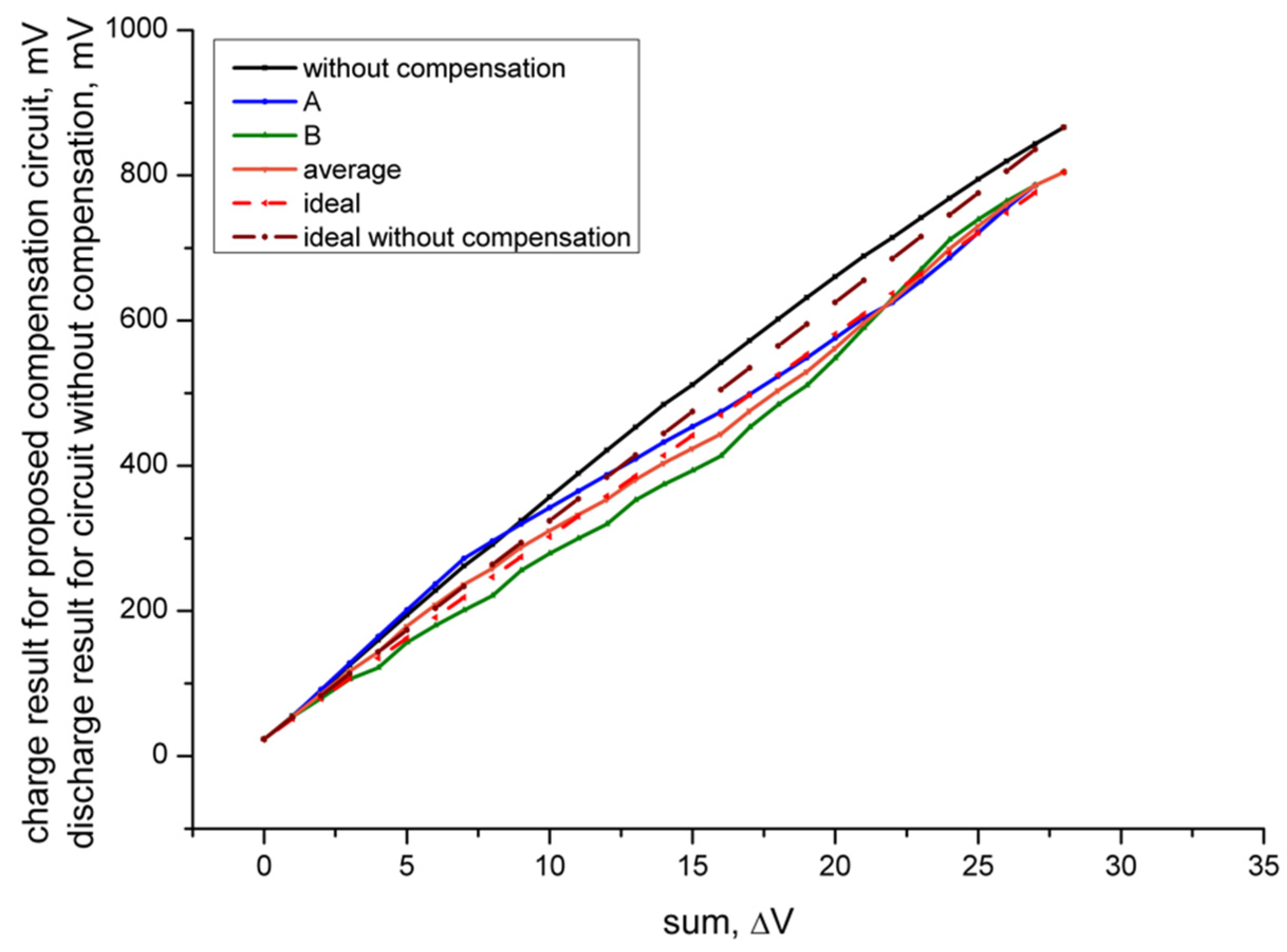
18]. This makes the proposed compensation circuit suitable for use in a wider range, but this causes a new case to emerge: the same accumulation result can be achieved in multiple ways. For example, 16 can be achieved through 4 + 4 + 4 + 4 or 7 + 7 + 2 + 0. All combinations were tested, and the results are shown in
Figure 4.
Waves A and B mark the largest and smallest charge results achievable through all combinations, respectively, which were often obtained when the four inputs were the same or when inputs had the most differences. We believe this was because there was still a minor difference in the balanced voltage of the bitline depending on the number of activated wordlines, which caused every cell to have a slightly different discharge current. In addition, charge currents from cells that stored the high-voltage state also affected the computing process. These charge currents were normally small enough to be ignored, but still influenced the result. The average charge amount for the different combinations is also plotted through the wave labelled “average”. The ideal wave is a line with an average result of 0 and 28 at its two ends; it is used to calculate the integral nonlinearity (INL) values of the result wave. The wave labelled “without compensation” is the discharge result of the result capacitor when conventional methods were used, as shown in
Figure 2a. The “ideal without compensation” wave is the calculated wave using conventional methods.
Figure 4 gives a general picture of the resulting voltages with different calculation factors. When comparing the lines with and without compensation, it is clear that nonlinearity dropped. This is shown by the small difference between the tested data lines and the calculated ideal lines. Both A and B had a smaller average INL compared to that without compensation, as well as average test data close to the ideal calculated data, which could be achieved with just a minor decrease in output voltage swing as sacrifice. This is shown in
Figure 4, as waves A, B, and “average” are closer to the ideal wave than the “without compensation” wave is to the “ideal without compensation” wave.
The INL values of the results can reflect their linearity, which is calculated through:
where LSB is the least significant bit—the ideal unit of change between two adjacent results. We tally the INL of our results and the results of [
12,
13] in
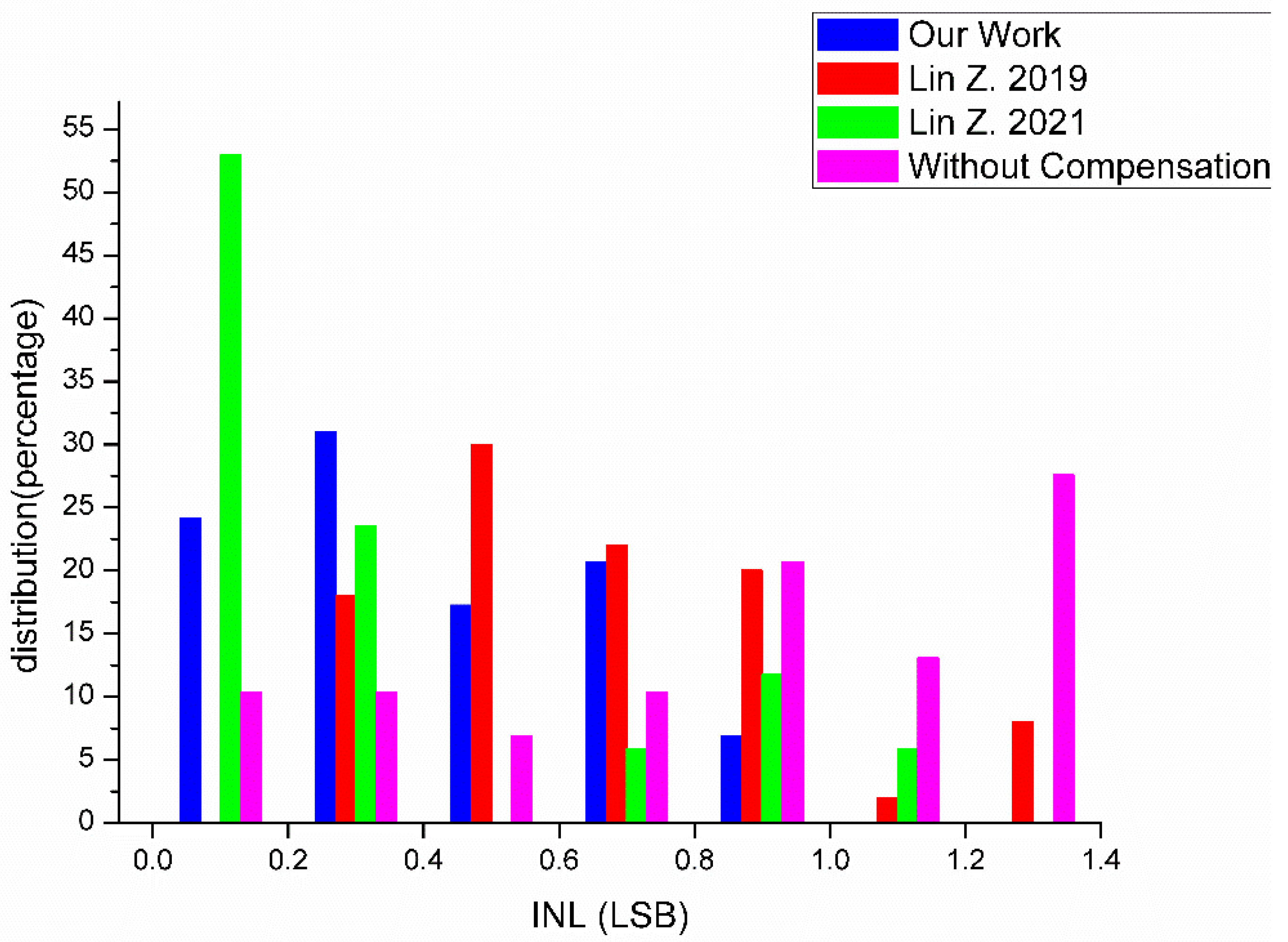
Figure 5, which are all under tt corner conditions and 25 °C The INL of our results was calculated using the data for the calculated ideal line as the Ideal Value and the average result voltage of all possible calculation combinations as the Tested Value. The INL from [
13] are under the conditions of VDD = 0.8 V and Last Column in their article, respectively. The INL of the results without a compensation circuit was obtained using the SRAM cells in our design, as the results vary when using different technologies. Using our own, under 55 nm technology, would be better for comparison. As in
Figure 5, only all the INLs of our work are lower than 1 LSB, indicating a considerable increase in precision. If an ADC were used to convert the compute result as in conventional CIM designs, the error in the digital data converted would be equal to or less than one minimum bit variation.
For a more detailed analysis, results of INL using the proposed circuit under different conditions were simulated and are presented in
Table 1. The average INL when using the proposed compensation circuit was 0.403 LSB under tt corner and 25 °C. There was a 51.2% drop from the average INL when no measures were used, which was 0.826 LSB under the same conditions. The average INL of the maximum and minimum charge results under different combinations was 0.65 LSB and 0.77 LSB, both improved from the INL with no measurements. Temperature had a similar effect on the INL as corner. The influence of both temperature and corner on INL was not severe and could be optimized by adjusting the reference voltage of the following A/D module, which is a very common scheme used in CIM designs. Other conditions that might influence the INL were also tested, including the size of the SRAM array. SRAM arrays with rows of 4, 8, 16, and 32 were tested for influence, and the results suggest that this was not a main factor as there was less than a 1% change in INL and voltage output swing. The linearity improvement of the proposed design is innovative, as it is achieved under flexible wordline activation and wide voltage output swing.
5. Discussion
The analog compute process is the core of most CIM designs, especially mixed-signal SRAM-based CIMs, which often use multi-row read operations for computing. Most peripheral CIM circuits, including the circuit proposed in this article, are modules for optimizing this analog compute process. However, this is a multi-goal process, so many factors should be considered as a whole in order to give an objective appraisal for such a module. The factors that we believe to be crucial are listed in
Table 2. These factors can be sorted into two main groups.
The first group are factors that affect the result of analog computing directly, including linearity, output bits, and output swing. Linearity is a decisive factor for the precision of the result and is represented through INL, as is written in the section above. Output bits is a factor to be considered, as the affect for 1 LSB is much more severe for a low-bit output than for a high-bit output. The output bits of a design stand for the bit width that the output swing can represent. Output bits can be a decimal rather than an integer, as addition is included in the calculation. For example, in our design, four 3 bit inputs are each multiplied with a 1 bit input and then added together, leading to a 0 to 28 decimal or 4.8125 binary bit result. The output swing is also an important factor, as a larger output swing means that there is a larger interval between two adjacent results. This means that there is less designing difficulty on following modules, normally an A/D module to quantify the correct value. Although different designs have differences in supply voltage, the pressure on A/D module resolution does not change, making output swing a comparable factor. To combine these factors, a figure of merit (FOM) is proposed for direct assessment, as follows:
A smaller FOM indicates a better performance in analog computing for the assessed module. Our proposed compensation circuit, which should also be accounted as an analog compute module, had a smaller FOM compared to schemes with similar purposes, as shown in
Table 2.
The second group are factors that do not affect the computing result directly, but have an impact on stability, flexibility, or performance. Clamp voltage is a crucial function in charge domain CIM designs. The voltage of the bitline is clamped during the compute process, which ensures a stable discharge current. Adjustability refers to whether the design can be used under different technologies through simple modification. Some designs are difficult to adapt when the technology used changes. Input flexibility is an important indicator for the generality of the design. In some designs, the input for every wordline is fixed, as they can only be 0 or a certain amount. This is often to set a starting and ending signal for purposes such as triggering the compute phase or activating compensation circuits. However, fixed inputs minimize the ability to solve different types of computation and narrow the application of the design. Computing leakage current is also an important factor. It refers to the computing leakage current created by the analog computing module, which is often greater than the SRAM leakage current and has effect on the computing result. The computing leakage current is often not mentioned and statistics are rarely given in similar research papers. This leakage is often large during the standby stage of computing methods, either before or after the activation of wordlines when actual computation does not take action inside the compute phase. Unlike the SRAM leakage current in the read operation of normal SRAMs, the computing leakage current is not heavily influenced by the size of the SRAM array in our proposed design. This is because the leakage caused by deactivated SRAM cells can be adjusted by the proposed compensation circuit and is a part of the discharge current during the CIM multi-row read operation. In our design, an additional switch between the SRAM array and the analog compute module minimizes the leakage caused by the compensation circuit during ordinary SRAM operations, such as read and write operations.
A comparison of the proposed compensation circuit and other analog compute modules is provided in
Table 2, which shows the differences in the factors mentioned above. We also compared our design with designs using advanced technology nodes, such as [
11]. The results show that the FOM of our design was better, so there is no evidence that a better overall analog compute result can be obtained by using a more advanced technology node.
6. Conclusions
In this work, we propose the use of a new compensation circuit in CIM multi-row read operations, which has comprehensive significance. It can clamp the bitline voltage, and is adaptable to flexible inputs and different technologies. The computing leakage current caused by the circuit was relatively small and did not affect the computation results. It had a wide-swing output and high overall linearity. The compensation circuit does not affect regular SRAM read and write processes, which are controlled by a switch between the bitlines and the analog compute module. A FOM was proposed for the purpose of direct comparison. In the FOM proposed, the compensation circuit was advantageous over other schemes and modules, indicating good analog computing performance. The proposed design was designed with 55 nm CMOS technology and showed significant improvement in power consumption, output swing, and computation linearity. Our proposed circuit could satisfy the demand of multi-row reading in the general context of SRAM-based mixed-signal CIM designs. In the future, we plan to test our proposed circuit with different CIM structures, including CIMs not based on SRAM.
Author Contributions
Conceptualization, Z.G.; methodology, Z.G.; software, S.Q.; validation, Z.G. and S.Q.; formal analysis, Z.G.; investigation, Z.G.; resources, S.Q.; data curation, Z.G. and S.Q.; writing—original draft preparation, Z.G.; writing—review and editing, Z.G., H.Z. and S.Q.; supervision, H.Z., X.W. and S.Q.; project administration, Y.Z. All authors have read and agreed to the published version of the manuscript.
Funding
This research received no external funding.
Conflicts of Interest
The authors declare no conflict of interest.
References
- Sumbul, H.E.; Chen, G.K.; Knag, P.C.; Kumar, R.; Anders, M.A.; Kaul, H.; Hsu, S.K.; Agarwal, A.; Kar, M.; Kim, S.; et al. A 2.9–33.0 TOPS/W Reconfigurable 1-D/2-D Compute-Near-Memory Inference Accelerator in 10-nm FinFET CMOS. IEEE Solid-State Circuits Lett. 2020, 3, 118–121. [Google Scholar] [CrossRef]
- Santoro, G.; Turvani, G.; Graziano, M. New Logic-In-Memory Paradigms: An Architectural and Technological Perspective. Micromachines 2019, 10, 368. [Google Scholar] [CrossRef] [PubMed] [Green Version]
- Ottati, F.; Turvani, G.; Masera, G.; Vacca, M. Custom Memory Design for Logic-in-Memory: Drawbacks and Improvements over Conventional Memories. Electronics 2021, 10, 2291. [Google Scholar] [CrossRef]
- Biswas, A.; Chandrakasan, A.P. CONV-SRAM: An Energy-Efficient SRAM With In-Memory Dot-Product Computation for Low-Power Convolutional Neural Networks. IEEE J. Solid-State Circuits 2019, 54, 217–230. [Google Scholar] [CrossRef] [Green Version]
- Si, X.; Xue, C.-X.; Su, J.-W.; Zhang, Z.; Li, S.-H.; Sheu, S.-S.; Lee, H.-Y.; Chen, P.-C.; Wu, H.; Qian, H.; et al. Circuit Design Challenges in Computing-in-Memory for AI Edge Devices. In Proceedings of the IEEE 13th International Conference on ASIC, ASICON, Chongqing, China, 29 October–1 November 2019. [Google Scholar]
- Agrawal, A.; Jaiswal, A.; Lee, C.; Roy, K. X-SRAM: Enabling In-Memory Boolean Computations in CMOS Static Random Access Memories. IEEE Trans. Circuits Syst. I Regul. Pap. 2018, 65, 4219–4232. [Google Scholar] [CrossRef] [Green Version]
- Yadav, N.; Kim, Y.; Li, S.; Choi, K.K. Stable, Low Power and Bit-Interleaving Aware SRAM Memory for Multi-Core Processing Elements. Electronics 2021, 10, 2724. [Google Scholar] [CrossRef]
- Yu, C.; Yoo, T.; Kim, T.T.; Tshun Chuan, K.C.; Kim, B. A 16K Current-Based 8T SRAM Compute-In-Memory Macro with Decoupled Read/Write and 1-5bit Column ADC. In Proceedings of the 2020 IEEE Custom Integrated Circuits Conference, CICC, Boston, MA, USA, 22–25 March 2020. [Google Scholar]
- Kang, M.; Keel, M.-S.; Shanbhag, N.R.; Eilert, S.; Curewitz, K. An energy-efficient VLSI architecture for pattern recognition via deep embedding of computation in SRAM. In Proceedings of the 2014 IEEE International Conference on Acoustics, Speech and Signal Processing, ICASSP, Florence, Italy, 4–9 May 2014. [Google Scholar]
- Su, J.-W.; Si, X.; Chou, Y.-C.; Chang, T.-W.; Huang, W.-H.; Tu, Y.-N.; Liu, R.; Lu, P.-J.; Liu, T.-W.; Wang, J.-H.; et al. 15.2 A 28nm 64Kb Inference-Training Two-Way Transpose Multibit 6T SRAM Compute-in-Memory Macro for AI Edge Chips. In Proceedings of the 2020 IEEE International Solid-State Circuits Conference, ISSCC, San Francisco, CA, USA, 16–20 February 2020. [Google Scholar]
- Sinangil, M.E.; Erbagci, B.; Naous, R.; Akarvardar, K.; Sun, D.; Khwa, W.-S.; Liao, H.-J.; Wang, Y.; Chang, J. A 7-nm Compute-in-Memory SRAM Macro Supporting Multi-Bit Input, Weight and Output and Achieving 351 TOPS/W and 372.4 GOPS. IEEE J. Solid-State Circuits 2021, 56, 188–198. [Google Scholar] [CrossRef]
- Lin, Z.; Fang, Y.; Peng, C.; Lu, W.; Li, X.; Wu, X.; Chen, J. Current mirror-based compensation circuit for multi-row read in-memory computing. Electron. Lett. 2019, 55, 1176–1178. [Google Scholar] [CrossRef]
- Lin, Z.; Zhan, H.; Chen, Z.; Peng, C.; Wu, X.; Lu, W.; Zhao, Q.; Li, X.; Chen, J. Cascade Current Mirror to Improve Linearity and Consistency in SRAM In-Memory Computing. IEEE J. Solid-State Circuits 2021, 56, 2550–2562. [Google Scholar] [CrossRef]
- Jaiswal, A.; Chakraborty, I.; Agrawal, A.; Roy, K. 8T SRAM Cell as a Multibit Dot-Product Engine for Beyond Von Neumann Computing. IEEE Trans. Very Large Scale Integr. (VLSI) Syst. 2019, 27, 2556–2567. [Google Scholar] [CrossRef] [Green Version]
- Si, X.; Tu, Y.-N.; Huang, W.-H.; Su, J.-W.; Lu, P.-J.; Wang, J.-H.; Liu, T.-W.; Wu, S.-Y.; Liu, R.; Chou, Y.-C.; et al. 15.5 A 28nm 64Kb 6T SRAM Computing-in-Memory Macro with 8b MAC Operation for AI Edge Chips. In Proceedings of the 2020 IEEE International Solid-State Circuits Conference, ISSCC, San Francisco, CA, USA, 16–20 February 2020. [Google Scholar]
- Gonugondla, S.K.; Kang, M.; Shanbhag, N.R. A Variation-Tolerant In-Memory Machine Learning Classifier via On-Chip Training. IEEE J. Solid-State Circuits 2018, 53, 3163–3173. [Google Scholar] [CrossRef]
- Bansal, M.; Singh, H.; Sharma, G. A Taxonomical Review of Multiplexer Designs for Electronic Circuits & Devices. J. Electron. Inform. 2021, 3, 77–79. [Google Scholar]
- Kang, M.; Gonugondla, S.K.; Patil, A.; Shanbhag, N.R. A Multi-Functional In-Memory Inference Processor Using a Standard 6T SRAM Array. IEEE J. Solid-State Circuits 2018, 53, 642–655. [Google Scholar] [CrossRef]
- Jain, S.; Lin, L.; Alioto, M. ±CIM SRAM for Signed In-Memory Broad-Purpose Computing from DSP to Neural Processing. IEEE J. Solid-State Circuits 2021, 56, 2981–2992. [Google Scholar] [CrossRef]
| Publisher’s Note: MDPI stays neutral with regard to jurisdictional claims in published maps and institutional affiliations. |
© 2022 by the authors. Licensee MDPI, Basel, Switzerland. This article is an open access article distributed under the terms and conditions of the Creative Commons Attribution (CC BY) license (https://creativecommons.org/licenses/by/4.0/).


