Article

Broadband and Wide-Angle Performance of a Perfect Absorber Using a MIM Structure with 2D MXene

1
Key Laboratory of Optoelectronic Devices and Systems of Ministry of Education and Guangdong Province, College of Physics and Optoelectronic Engineering, Shenzhen University, Shenzhen 518060, China
2
International Collaborative Laboratory of 2D Materials for Optoelectronic Science & Technoloy of Ministry of Education, Shenzhen University, Shenzhen 518060, China
*
Author to whom correspondence should be addressed.
Electronics 2022, 11(9), 1370; https://doi.org/10.3390/electronics11091370
Submission received: 16 March 2022 / Revised: 18 April 2022 / Accepted: 21 April 2022 / Published: 25 April 2022
(This article belongs to the Special Issue Digital and Optical Security Algorithms via Machine Learning)

Abstract

:
Due to the extraordinary optoelectronic properties and surface-rich functional groups, MXene has shown great promise in many applications, such as electromagnetic shielding, catalysis, sensors, ultrafast photons, etc. In this work, we propose a wide-angle absorber based on a metal-insulator-metal (MIM) metamaterial consisting of MXene. By optimizing the design, the absorption efficiency can be further improved throughout the entire wavelength range. More importantly, the absorber exhibits high-efficiency broadband and wide-angle (20–80°) absorption in the near-infrared range (NIR: 1.1–1.7 μm) by numerical calculation. It is foreseeable that the excellent absorption characteristics and easy-to-manufacture structure of the designed absorber will bring some inspiration to the absorption device in the NIR and its practical application.

1. Introduction

With the development of science and technology, perfect absorbers have played a significant role in more and more fields, especially in solar cells, photoelectric detection, military stealth, etc. [1,2,3,4] In general, noble metals (such as Au and Ag) have been widely used as plasma absorbents [5,6]. Recently, two-dimensional (2D) materials, such as graphene, have been used as a promising absorbing material because of their unique light-absorption properties [7]. In addition, researchers have proposed many kinds of structures based on 2D materials to improve the absorption of photons [5,8,9]. For instance, we proposed a one-dimensional (1D), topological, photonic crystal heterostructure with graphene, which achieves perfect absorption in multiple channels [9]. The use of plasmon resonance in 2D materials for creating metasurface devices is an especially interesting research topic [10,11]. In fact, the absorption bandwidth is a heavy parameter for the absorber. However, a large amount of current research work relies on complex, 2D periodic structures to achieve miniaturized broadband, multi-channel, and other technical parameters [12]. In addition, the adjustable perfect absorber is an important aspect [13,14]. However, complex, multilayer, patterned structures have certain problems in quantitative production, and their manufacturing costs are relatively high. Therefore, developing the perfect absorber with a simple structure and economic cost is a key research direction.
More recently, the rising star of the 2D material family, 2D MXene, a ternary carbide or nitride with an anisotropic laminated structure, has successfully attracted the attention of a large number of researchers. Two-dimensional MXene has the general formula Mn+1XnTX, where n = 1, 2, or 3, M is a transition metal (e.g., Ti, Sc, V, Zr, Mo, Cr, and Nb), X is N or C, and TX is a surface functional group (e.g., OH, O, and F). Ti3C2Tx, as the most common and frequently studied member of the MXene family, has been applied in many fields due to its extraordinary properties [15,16], including all-optical modulation [17,18], ultrafast photons [19,20], transparent electrodes, [21], batteries [22], supercapacitors [23], sensors [24,25], and electromagnetic shielding [26,27]. Compared with traditional absorbing materials, 2D Ti3C2Tx has many unique advantages. First, it has a large surface area/volume ratio, which can improve interfacial polarization, scattering, and reflection of light waves between surfaces [28]. Second, it can be used as an impedance matching regulator and provide the best structure [29]. In addition, it has a lower density and can be used to design and prepare many types of structures [30]. The current research on the optical properties of Ti3C2Tx focuses on the high transmittance in the visible light spectrum [31,32]. In fact, in NIR, Ti3C2Tx exhibits characteristics similar to precious metal nanoparticles, and its bulk plasmon peak does not change with the size of the nanoparticles [33,34].
In this article, we designed a perfect absorber based on the MIM structure in the NIR range. The simulation results indicate that the change of the external refractive index of the resonance absorption peak is not sensitive over the wide-angle range. By changing the groove depth, the absorption is further improved. In addition, the absorber also exhibits polarization sensitivity and broadband characteristics.

2. Simulation Results and Discussions

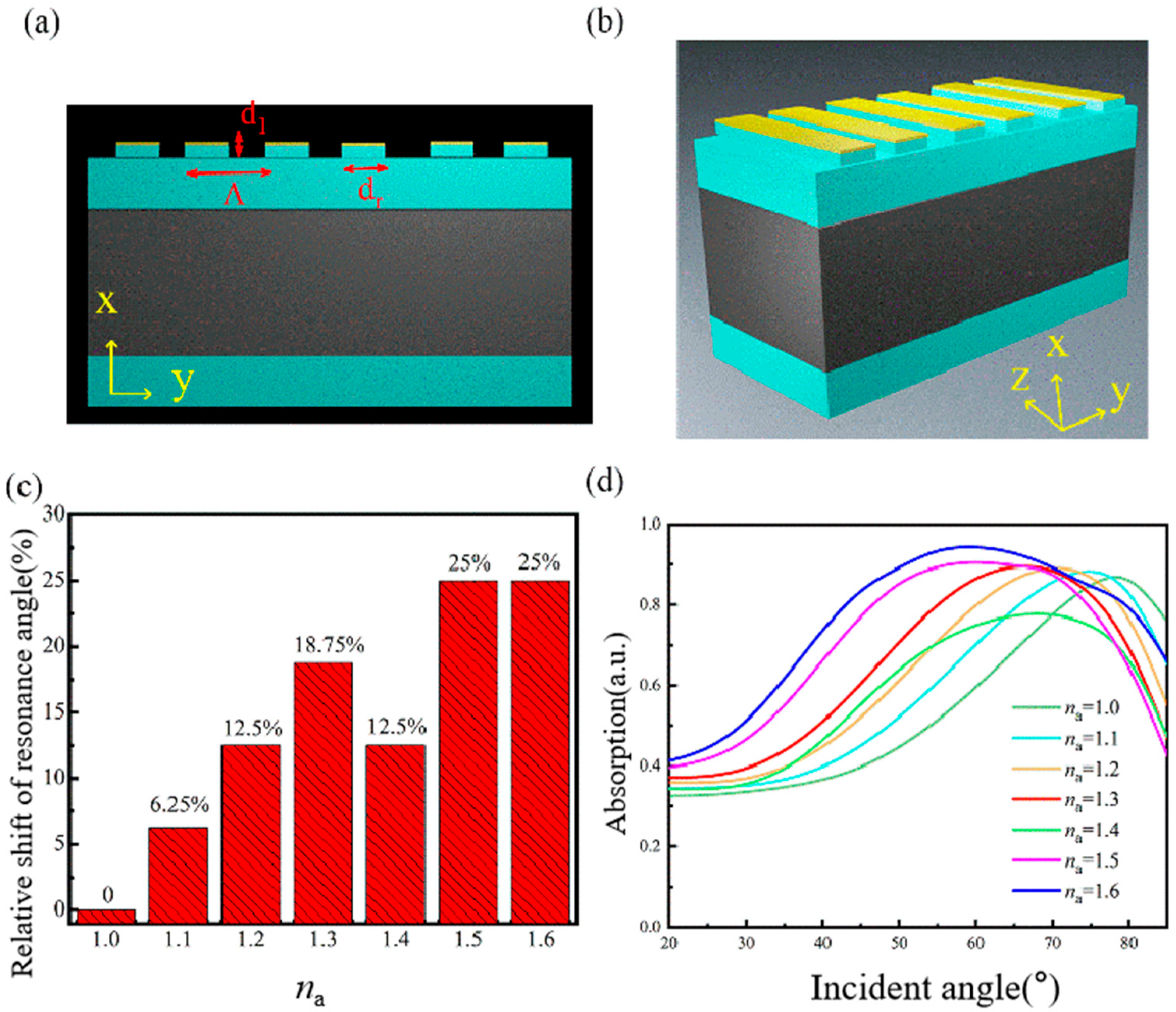
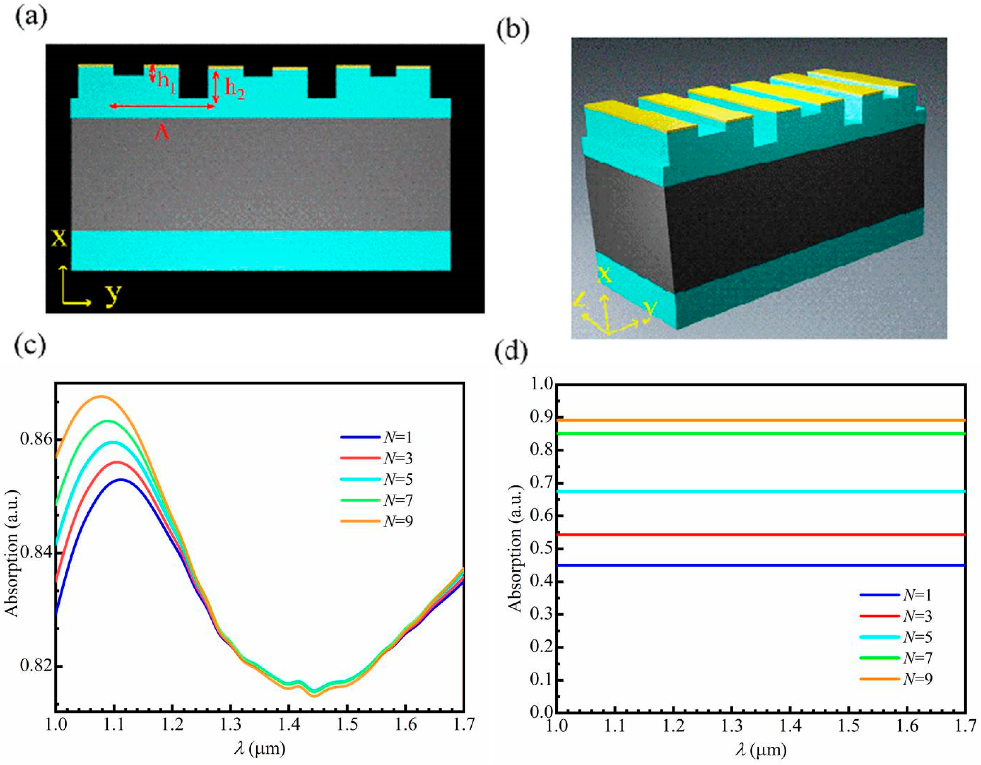
2.1. Structural Design

We performed electromagnetic analysis using the commercial software COMSOL Multiphysics 5.5 for numerical simulation. We used periodic boundary conditions in the Y-direction to simulate the propagation of light through an infinite, periodic nanostructure with open boundaries in the X-direction, the plane wave incident; the perfect matching layer is located at the periodic boundary of the structure, and the mesh accuracy is 1 nm. The plane wave is incident in the YOZ plane from the X-axis. The structure we designed is shown in Figure 1a,b. The dielectric layer is sandwiched between two layers of Ti3C2Tx, and a groove of height h is engraved on the top of the Ti3C2Tx. The width of the groove dr is 2.7 μm. We applied a protective layer of MgF2 on the top layer to prevent oxidation of the Ti3C2Tx. The MXene dielectric constant model in the literature was used to consider the experiment using MXene instead of simulating commonly used materials [26]. The period Λ = 3 μm, the thickness d1 of the upper Ti3C2Tx is 75 nm, and the dielectric constant of the Ti3C2Tx came from the literature [29]. The thickness d of the dielectric layer is 285 nm, and the refractive index is: n = 1.482 [35]. The angle of incidence was chosen to be 50°. In this work, we used the finite element method to simulate the light field distribution of the structure in the NIR range (1.0–1.7 μm). We used a 2D-simulation model (assuming the structure extends indefinitely in the Y-direction), set the X-direction as the periodic boundary condition, and set the Z-direction as the periodic port. Figure 1c shows the relative shift (θa − θ0)/θ0 × 100% of the resonance angle when the na changes at 1.0 μm, where, θa and θ0 are the resonance angles when the external refractive index is na and n0, respectively. For instance, θ0 = 80° is the resonance angle when na = 1.0. It was found that, when the external refractive index changes, the maximum resonance angle is only 25%. Simulation results show that the structure’s external refractive index change (na = 1.0–na = 1.6) has only a slight effect on its absorption capacity (Figure 1d).

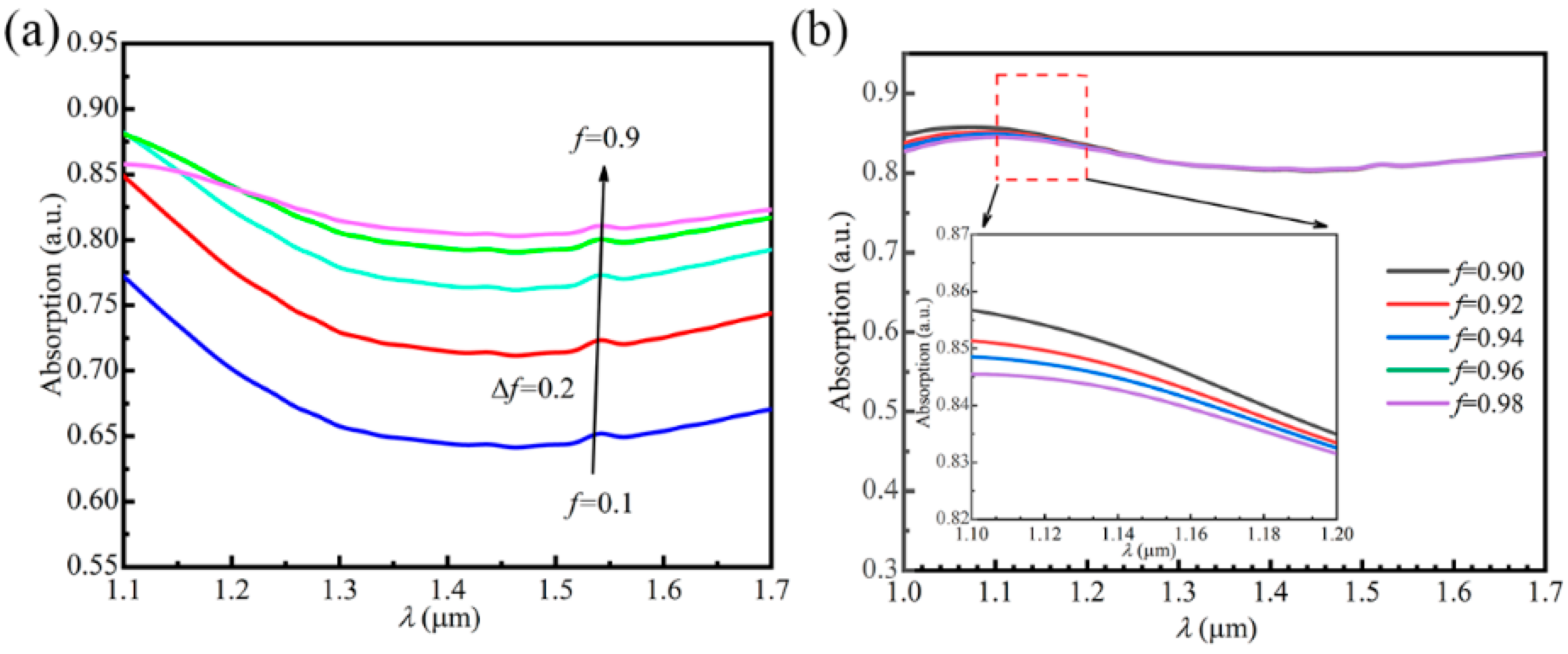
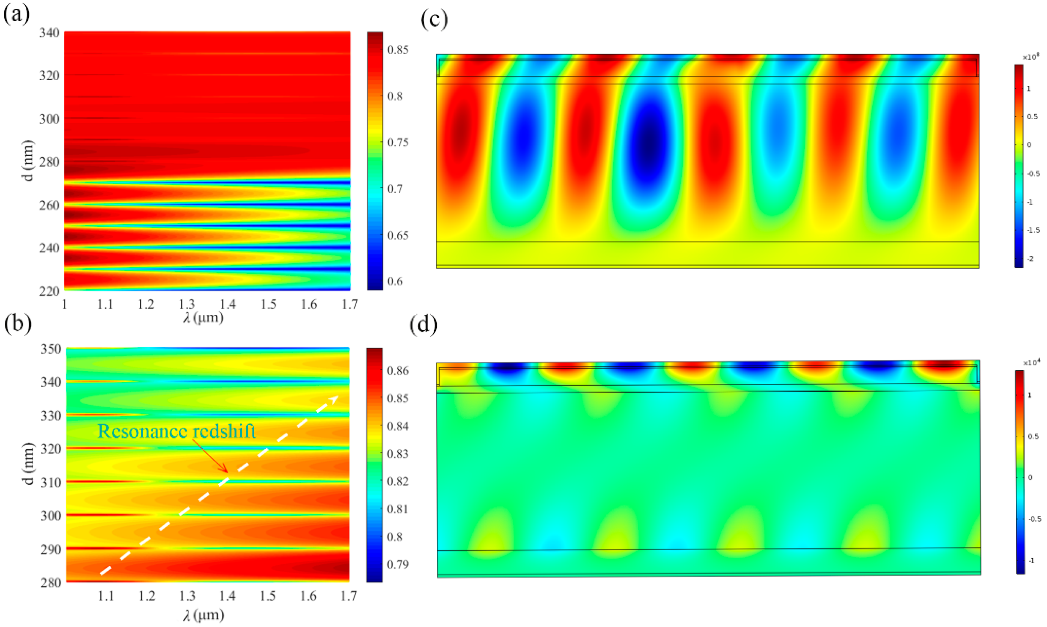
2.2. Broadband Analysis

In order to further improve the absorption performance of the structure, we considered the effects of the filling factor f and the thickness of the dielectric layer d on the absorption. We define the filling factor f as the length of the ridge divided by the grating period (f = d r Λ ). For a one-dimensional periodic grating structure, the parameters affecting system performance mainly include the width of the grating, the thickness of the dielectric layer, and the grating period. Taking TM polarized light as an example, the magnetic field of the incident light and the induced magnetic polaron resonate at this time so that the energy can be effectively confined in the absorber. Figure 2a shows the structure of the absorption diagram when f changes from 0.1 to 0.9, and it was found that, when f gradually increases, the absorption of the structure also increases. Figure 2b plots the absorption when f > 0.9. It was found that, when f was increased again, the overall absorption was basically unchanged and showed a slight downward trend. This may be because, as f increases, the relative area of the entire structure receiving light decreases. In fact, f = 1.0 is the flat structure of MXene, which also shows that the grating structure of MXene has a better absorption effect than the flat structure. When f = 0.9, the whole band has an absorption of 82%, which is the optimal solution for the absorption effect of the structure. Figure 3a shows the relationship between wavelength and absorption under different dielectric-layer thicknesses. It was found that the dielectric layer was too thin, and the absorption decreased (<60%). When d is between 280–290 nm, the absorption rate is as high as about 85%. The effect of the surface plasmon resonance cannot be excited under the change of the angle. Figure 3b shows that, when d > 280 nm, as the thickness of the dielectric layer increased, a resonance redshift occurred in the absorption. This redshift was due to the excessively thick dielectric layer, which resulted in a guided mode resonance (GMR) formed by the upper MXene grating and the dielectric layer, and the lower dielectric layer and the MXene plate [36,37].
In order to reveal the physical mechanism of the proposed broadband absorber, we calculated the electric and magnetic field energy distributions of the absorption spectrum at a wavelength of λ = 1.55 μm. Figure 3c,d show the absorption spectra in TE and TM modes in the electric field E_x, respectively. It was found that the electric field energy was about four orders of magnitude greater than the magnetic field energy, suggesting that electric field resonance dominates broadband absorption. We can see from Figure 3c,d that the energy of the electromagnetic field is hardly distributed on the MXene at the bottom. The electric field distribution in Figure 3c is mainly concentrated on the top of the grating, especially the grating slits, the corner portions of the Mxene, and the intermediate dielectric layer. The electric field distribution indicates that the appearance of the cavity mode is due to the MXene’s local surface plasmon resonance (LSP) and the structure’s guided mode resonance (GMR). It can be seen from Figure 3d that the magnetic field distribution is mainly concentrated on the top. In the above studies, we found that increasing the fill factor f can increase the absorption rate of the absorber, while the etching depth of the waveguide rib has no significant effect on the absorption rate (Figure 4c). In the grating structure, generally through the structure, adjust to an asymmetrical groove profile or multi-layer step grating to improve the absorption coupling efficiency [38,39,40,41,42]. Therefore, we considered setting the waveguide rib etching depth h to different heights and found that the absorption was significantly enhanced. Here, we consider setting the waveguide rib etch depth to a different height.
Figure 4a,b shows the structure we designed. One should note the change in the absorption of the structure when the other parameters of h2 remained the same as those in Figure 1a. We defined relative height N = h2/h1. Figure 4c,d shows the effect of waveguide rib etch depth on absorption in TM and TE polarization mode. Since only TM polarization supports surface plasmon resonance, it is seen that the absorption in TM mode varies with wavelength: the absorption rate fluctuated (Figure 4c), while the wavelength in TE mode had no effect on absorption (Figure 4d). In order to compare the waveforms under TM and TE polarization more intuitively, the angle of incidence was kept at 50° (Figure 4c,d). Although the excitation mechanism under the polarization of TM and TE is different, it can be seen that the change trend of the two is consistent; that is, as N increases, the absorption rate increases. Because f is calculated based on periodic boundary conditions, we maintain the same as the optimal structural parameters in Figure 1 (f = 0.9). We changed the waveguide rib etch depth, which is equivalent to linearly superimposing two single grating structures with different waveguide rib etch depths. Figure 5a shows the absorption change of the structure at the symmetrical height and the asymmetrical height (n = 4). It was found that changing h2 does improve the absorption. It can be seen that, after greater than 1.3 μm, the absorption is stable; the two improved nearly 14%. In order to more clearly show the system performance under this asymmetric structure, we show the relationship between the wavelength and the absorption as f changes in Figure 5b,c, respectively. Taking f = 0.4 and f = 0.2 as examples, the wavelength and absorption under other conditions have a similar relationship. It was found that, when f is reduced, it only affects the minimum value of energy absorption in the shorter wavelength range (1.0–1.2 μm) and has almost no effect on the band greater than 1.2 μm.

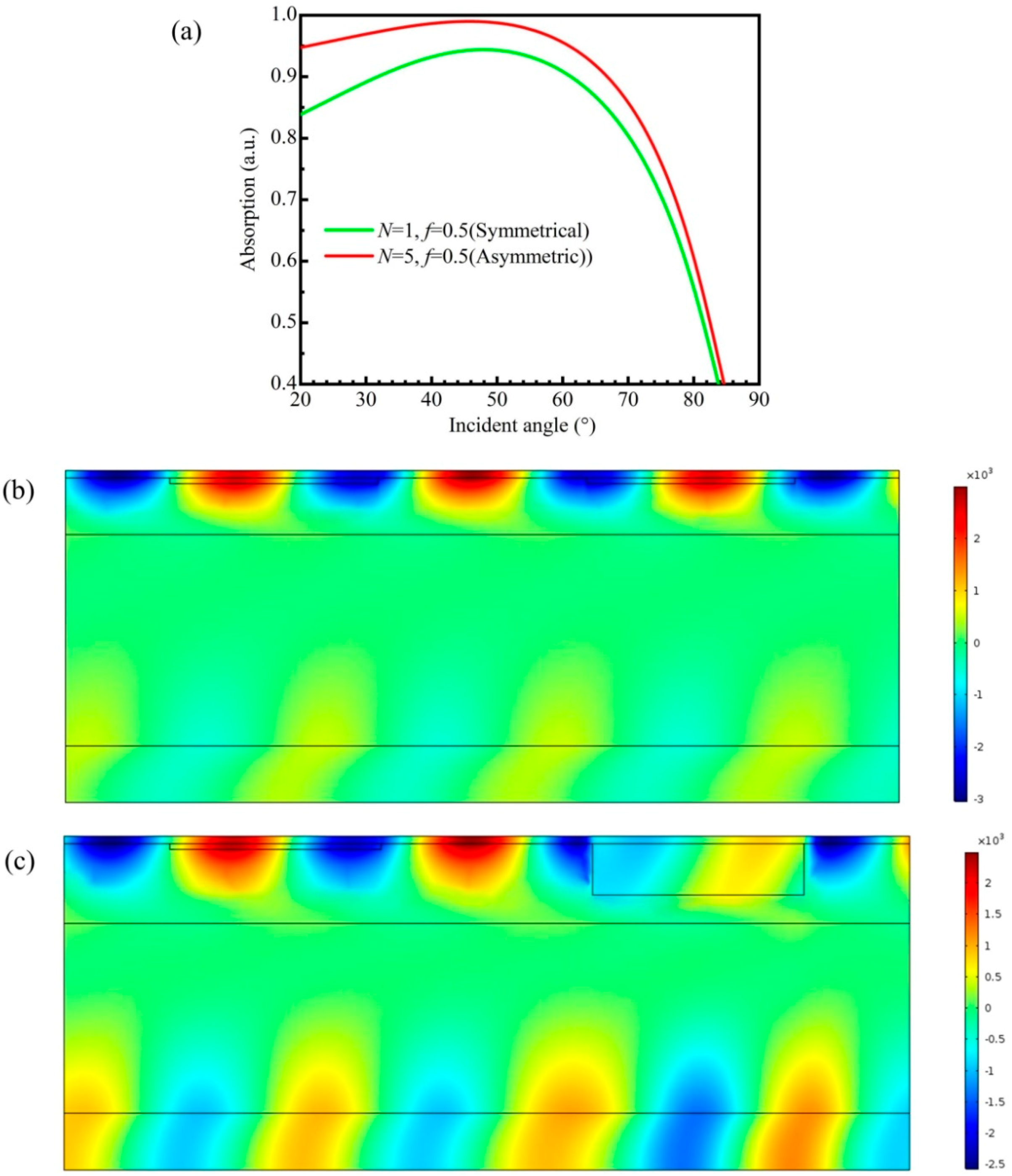
2.3. Wide-Angle Analysis

In the previous discussion, we observed the absorption characteristics of this structure over a wideband. In order to investigate whether the structure has more perfect performance, we studied its wide-angle absorption performance because surface plasmon resonance can only be excited in TM mode, and it has been shown in Figure 4d that TE mode cannot effectively achieve perfect absorption. Therefore, we only discuss the wide angle of the absorption performance of the structure in TM mode. The simulation results show that the etching depth of the asymmetric waveguide rib (n = 5) can reach an absorption rate close to 1.0, while the symmetric structure (n = 1) can only achieve an absorption rate of about 90% at most with λ = 1.55 μm and f = 0.5 (See Figure 6a). In Figure 6b,c, we show the corresponding energy absorption diagrams of symmetric and asymmetric structures at λ = 1.55 μm and θ = 50°. There is only a small difference between the two structures.
Finally, we compare the other near-infrared bands based on the MIM structural properties of the absorber (Table 1). It can be seen from Table 1 that the absorber we designed based on the MIM structure has both broadband and wide-angle absorption performance, and the structure is simple, which is expected to be applied in actual production.

3. Conclusions

In our work, we have designed a broadband and wide-angle perfect absorber based on the new two-dimensional material, MXene. Compared with other similar absorbers, it performs excellently. The highlight of our work is to couple the extraordinary performance of the two-dimensional MXene with an asymmetrical grating to achieve a surprising effect. The absorption rate exceeds 80% in the angle range of at least 50–80, and the first rate of more than 80% can be achieved in the entire band of 1.1 μm−1.7 μm. In addition, it is simple and easy to manufacture, and miniaturized structures are more likely to be used in practical applications. It is expected that our research can be applied to equipment and heat radiators in the field of photovoltaic design.

Author Contributions

Y.J. is work on Conceptualization, and Writing Original Draft, C.S. is work on Investigation, Y.L. is work on Software, and H.C. is work on Project administration. All authors have read and agreed to the published version of the manuscript.

Funding

This work is supported by National Natural Science Foundation of China (NSFC) (11775147); Guangdong Basic and Applied Basic Research Foundation (Nos. 2019A1515011474 and 2019A1515110130); Shenzhen Science and Technology Program (Nos. JCYJ20210324095007020, JCYJ20200109105201936 and JCYJ20190808115605501).

Conflicts of Interest

The authors declare that they have no conflicts of interest.

References

  1. Yan, H.; Li, X.; Chandra, B.; Tulevski, G.; Wu, Y.; Freitag, M.; Zhu, W.; Avouris, P.; Xia, F. Tunable Infrared Plasmonic Devices Using Graphene/Insulator Stacks. Nat. Nanotechnol. 2012, 7, 330–334. [Google Scholar] [CrossRef] [PubMed] [Green Version]
  2. Chou Chau, Y.-F.; Chou Chao, C.-T.; Huang, H.J.; Kooh, M.R.R.; Kumara, N.T.R.N.; Lim, C.M.; Chiang, H.-P. Perfect Dual-Band Absorber Based on Plasmonic Effect with the Cross-Hair/Nanorod Combination. Nanomaterials 2020, 10, 493. [Google Scholar] [CrossRef] [PubMed] [Green Version]
  3. Chao, C.-T.C.; Chau, Y.-F.C.; Chiang, H.-P. Enhancing plasmonic effect in periodic nanometal square prisms with fences and cavities for refractive index and temperature sensing applications. J. Nanoparticle Res. 2020, 22, 297. [Google Scholar] [CrossRef]
  4. Chou Chao, C.-T.; Chou Chau, Y.-F.; Chiang, H.-P. Biosensing on a Plasmonic Dual-Band Perfect Absorber Using Intersection Nanostructure. ACS Omega 2022, 7, 1139–1149. [Google Scholar] [CrossRef]
  5. Jiang, T.; Huang, Y.; Meng, X. Cds Core-Au/Mxene-Based Photodetectors: Positive Deep-Uv Photoresponse and Negative Uv–Vis-Nir Photoresponse. Appl. Surf. Sci. 2020, 513, 145813. [Google Scholar] [CrossRef]
  6. Liao, Y.; Shan, Y.; Wu, L.; Xiang, Y.; Dai, X. Liquid-Exfoliated Few-Layer Inse Nanosheets for Broadband Nonlinear All-Optical Applications. Adv. Opt. Mater. 2020, 8, 1901862. [Google Scholar] [CrossRef]
  7. Song, C.; Liao, Y.; Xiang, Y.; Dai, X. Liquid phase exfoliated boron nanosheets for all-optical modulation and logic gates. Sci. Bull. 2020, 65, 1030–1038. [Google Scholar] [CrossRef]
  8. Wang, X.; Jiang, X.; You, Q.; Guo, J.; Dai, X.; Xiang, Y. Tunable and Multichannel Terahertz Perfect Absorber Due to Tamm Surface Plasmons with Graphene. Photon. Res. 2017, 5, 536–542. [Google Scholar] [CrossRef]
  9. Wang, X.; Liang, Y.; Wu, L.; Guo, J.; Dai, X.; Xiang, Y. Multi-Channel Perfect Absorber Based on a One-Dimensional Topological Photonic Crystal Heterostructure with Graphene. Opt. Lett. 2018, 43, 4256–4259. [Google Scholar] [CrossRef]
  10. Wang, C.; Liang, J.; Cai, T.; Li, H.; Ji, W.; Zhang, Q.; Zhang, C. High-Performance and Ultra-Broadband Metamaterial Absorber Based on Mixed Absorption Mechanisms. IEEE Access 2019, 7, 57259–57266. [Google Scholar] [CrossRef]
  11. Othman, M.A.K.; Guclu, C.; Capolino, F. Graphene-Based Tunable Hyperbolic Metamaterials and Enhanced near-Field Absorption. Opt. Express 2013, 21, 7614–7632. [Google Scholar] [CrossRef] [PubMed] [Green Version]
  12. Lin, K.-T.; Lin, H.; Yang, T.; Jia, B. Structured Graphene Metamaterial Selective Absorbers for High Efficiency and Omnidirectional Solar Thermal Energy Conversion. Nat. Commun. 2020, 11, 1389. [Google Scholar] [CrossRef] [Green Version]
  13. Cui, Y.; Fung, K.H.; Xu, J.; Ma, H.; Jin, Y.; He, S.; Fang, N.X. Ultrabroadband Light Absorption by a Sawtooth Anisotropic Metamaterial Slab. Nano Lett. 2012, 12, 1443–1447. [Google Scholar] [CrossRef] [Green Version]
  14. You, W.; Pei, K.; Yang, L.; Li, X.; Shi, X.; Yu, X.; Guo, H.; Che, R. In Situ Dynamics Response Mechanism of the Tunable Length-Diameter Ratio Nanochains for Excellent Microwave Absorber. Nano Res. 2020, 13, 72–78. [Google Scholar] [CrossRef]
  15. Ghidiu, M.; Lukatskaya, M.R.; Zhao, M.-Q.; Gogotsi, Y.; Barsoum, M.W. Conductive Two-Dimensional Titanium Carbide ‘Clay’ with High Volumetric Capacitance. Nature 2014, 516, 78–81. [Google Scholar] [CrossRef] [PubMed]
  16. Ling, Z.; Ren, C.E.; Zhao, M.-Q.; Yang, J.; Giammarco, J.M.; Qiu, J.; Barsoum, M.W.; Gogotsi, Y. Flexible and Conductive Mxene Films and Nanocomposites with High Capacitance. Proc. Natl. Acad. Sci. USA 2014, 111, 16676. [Google Scholar] [CrossRef] [PubMed] [Green Version]
  17. Wu, L.; Jiang, X.; Zhao, J.; Liang, W.; Li, Z.; Huang, W.; Lin, Z.; Wang, Y.; Zhang, F.; Lu, S.; et al. Mxene-Based Nonlinear Optical Information Converter for All-Optical Modulator and Switcher. Laser Photonics Rev. 2018, 12, 1800215. [Google Scholar] [CrossRef]
  18. Wu, Q.; Huang, W.; Wang, Y.; Wang, C.; Zheng, Z.; Chen, H.; Zhang, M.; Zhang, H. All-Optical Control of Microfiber Knot Resonator Based on 2d Ti2ctx Mxene. Adv. Opt. Mater. 2020, 8, 1900977. [Google Scholar] [CrossRef]
  19. Jiang, X.; Liu, S.; Liang, W.; Luo, S.; He, Z.; Ge, Y.; Wang, H.; Cao, R.; Zhang, F.; Wen, Q.; et al. Broadband Nonlinear Photonics in Few-Layer Mxene Ti3c2tx (T = F, O, or Oh). Laser Photonics Rev. 2018, 12, 1700229. [Google Scholar] [CrossRef]
  20. Wu, Q.; Jin, X.; Chen, S.; Jiang, X.; Hu, Y.; Jiang, Q.; Wu, L.; Li, J.; Zheng, Z.; Zhang, M.; et al. Mxene-Based Saturable Absorber for Femtosecond Mode-Locked Fiber Lasers. Opt. Express 2019, 27, 10159–10170. [Google Scholar] [CrossRef]
  21. Halim, J.; Lukatskaya, M.R.; Cook, K.M.; Lu, J.; Smith, C.R.; Näslund, L.-Å.; May, S.J.; Hultman, L.; Gogotsi, Y.; Eklund, P.; et al. Transparent Conductive Two-Dimensional Titanium Carbide Epitaxial Thin Films. Chem. Mater. 2014, 26, 2374–2381. [Google Scholar] [CrossRef] [PubMed]
  22. Kajiyama, S.; Szabova, L.; Sodeyama, K.; Iinuma, H.; Morita, R.; Gotoh, K.; Tateyama, Y.; Okubo, M.; Yamada, A. Sodium-Ion Intercalation Mechanism in Mxene Nanosheets. ACS Nano 2016, 10, 3334–3341. [Google Scholar] [CrossRef]
  23. Lukatskaya, M.R.; Kota, S.; Lin, Z.; Zhao, M.-Q.; Shpigel, N.; Levi, M.D.; Halim, J.; Taberna, P.-L.; Barsoum, M.W.; Simon, P.; et al. Ultra-High-Rate Pseudocapacitive Energy Storage in Two-Dimensional Transition Metal Carbides. Nat. Energy 2017, 2, 17105. [Google Scholar] [CrossRef]
  24. Dai, X.; Song, C.; Qiu, C.; Wu, L.; Xiang, Y. Theoretical Investigation of Multilayer Ti3c2tx Mxene as the Plasmonic Material for Surface Plasmon Resonance Sensors in near Infrared Region. IEEE Sens. J. 2019, 19, 11834–11838. [Google Scholar] [CrossRef]
  25. Wu, L.; You, Q.; Shan, Y.; Gan, S.; Zhao, Y.; Dai, X.; Xiang, Y. Few-Layer Ti3c2tx Mxene: A Promising Surface Plasmon Resonance Biosensing Material to Enhance the Sensitivity. Sens. Actuators B Chem. 2018, 277, 210–215. [Google Scholar] [CrossRef]
  26. Kim, H.; Wang, Z.; Alshareef, H.N. Mxetronics: Electronic and Photonic Applications of Mxenes. Nano Energy 2019, 60, 179–197. [Google Scholar] [CrossRef]
  27. Shahzad, F.; Alhabeb, M.; Hatter, C.B.; Anasori, B.; Man Hong, S.; Koo, C.M.; Gogotsi, Y. Electromagnetic Interference Shielding with 2d Transition Metal Carbides (Mxenes). Science 2016, 353, 1137. [Google Scholar] [CrossRef] [PubMed] [Green Version]
  28. Chaudhuri, K.; Alhabeb, M.; Wang, Z.; Shalaev, V.M.; Gogotsi, Y.; Boltasseva, A. Highly Broadband Absorber Using Plasmonic Titanium Carbide (Mxene). ACS Photonics 2018, 5, 1115–1122. [Google Scholar] [CrossRef]
  29. Dillon, A.D.; Ghidiu, M.J.; Krick, A.L.; Griggs, J.; May, S.J.; Gogotsi, Y.; Barsoum, M.W.; Fafarman, A.T. Highly Conductive Optical Quality Solution-Processed Films of 2d Titanium Carbide. Adv. Funct. Mater. 2016, 26, 4162–4168. [Google Scholar] [CrossRef]
  30. Xiong, D.; Li, X.; Bai, Z.; Lu, S. Recent Advances in Layered Ti3c2tx Mxene for Electrochemical Energy Storage. Small 2018, 14, 1703419. [Google Scholar] [CrossRef] [Green Version]
  31. Zhang, C.; Anasori, B.; Seral-Ascaso, A.; Park, S.-H.; McEvoy, N.; Shmeliov, A.; Duesberg, G.S.; Coleman, J.N.; Gogotsi, Y.; Nicolosi, V. Transparent, Flexible, and Conductive 2d Titanium Carbide (Mxene) Films with High Volumetric Capacitance. Adv. Mater. 2017, 29, 1702678. [Google Scholar] [CrossRef]
  32. Xiong, K.; Wang, P.; Yang, G.; Liu, Z.; Zhang, H.; Jin, S.; Xu, X. Functional Group Effects on the Photoelectronic Properties of Mxene (Sc2ct2, T = O, F, Oh) and Their Possible Photocatalytic Activities. Sci. Rep. 2017, 7, 15095. [Google Scholar] [CrossRef] [PubMed] [Green Version]
  33. Tuo, M.; Xu, C.; Mu, H.; Bao, X.; Wang, Y.; Xiao, S.; Ma, W.; Li, L.; Tang, D.; Zhang, H.; et al. Ultrathin 2d Transition Metal Carbides for Ultrafast Pulsed Fiber Lasers. ACS Photonics 2018, 5, 1808–1816. [Google Scholar] [CrossRef]
  34. Aydin, K.; Ferry, V.E.; Briggs, R.M.; Atwater, H.A. Broadband Polarization-Independent Resonant Light Absorption Using Ultrathin Plasmonic Super Absorbers. Nat. Commun. 2011, 2, 517. [Google Scholar] [CrossRef] [PubMed]
  35. Gomes de Souza, I.L.; Rodriguez-Esquerre, V.F. Omnidirectional Broadband Absorber for Visible Light Based on a Modulated Plasmonic Multistack Grating. Opt. Laser Technol. 2020, 124, 105981. [Google Scholar] [CrossRef]
  36. Li, Y.; Liu, Z.; Zhang, H.; Tang, P.; Wu, B.; Liu, G. Ultra-Broadband Perfect Absorber Utilizing Refractory Materials in Metal-Insulator Composite Multilayer Stacks. Opt. Express 2019, 27, 11809–11818. [Google Scholar] [CrossRef]
  37. Feng, R.; Qiu, J.; Cao, Y.; Liu, L.; Ding, W.; Chen, L. Wide-Angle and Polarization Independent Perfect Absorber Based on One-Dimensional Fabrication-Tolerant Stacked Array. Opt. Express 2015, 23, 21023–21031. [Google Scholar] [CrossRef]
  38. Yang, Y.; Jia, H.; Bi, Y.; Zhao, H.; Yang, J. Experimental Demonstration of an Acoustic Asymmetric Diffraction Grating Based on Passive Parity-Time-Symmetric Medium. Phys. Rev. Appl. 2019, 12, 034040. [Google Scholar] [CrossRef] [Green Version]
  39. Bushuev, V.A.; Dergacheva, L.V.; Mantsyzov, B.I. Asymmetric Pendulum Effect and Transparency Change of PT-Symmetric Photonic Crystals under Dynamical Bragg Diffraction beyond the Paraxial Approximation. Phys. Rev. A 2017, 95, 033843. [Google Scholar] [CrossRef]
  40. Chau, Y.-F.C.; Chao, C.-T.C.; Huang, H.J.; Anwar, U.; Lim, C.M.; Voo, N.Y.; Mahadi, A.H.; Kumara, N.; Chiang, H.-P. Plasmonic perfect absorber based on metal nanorod arrays connected with veins. Results Phys. 2019, 15, 102567. [Google Scholar] [CrossRef]
  41. Chou Chau, Y.-F.; Lim, C.M.; Lee, C.; Huang, H.J.; Lin, C.-T.; Kumara, N.T.R.N.; Yoong, V.N.; Chiang, H.-P. Tailoring surface plasmon resonance and dipole cavity plasmon modes of scattering cross section spectra on the single solid-gold/gold-shell nanorod. J. Appl. Phys. 2016, 120, 093110. [Google Scholar] [CrossRef]
  42. Chau, Y.-F.C.; Chao, C.-T.C.; Huang, H.J.; Lim, R.C.; Chiang, H.-P. Tunable plasmonic effects arising from metal-dielectric nanorods. Appl. Opt. 2019, 58, 2530–2539. [Google Scholar] [CrossRef]
  43. Shi, Y.; Chen, X.; Lou, F.; Chen, Y.; Yan, M.; Wosinski, L.; Qiu, M. All-Optical Switching of Silicon Disk Resonator Based on Photothermal Effect in Metal&-Insulator-Metal Absorber. Opt. Lett. 2014, 39, 4431–4434. [Google Scholar] [PubMed]
  44. Dai, S.; Zhao, D.; Li, Q.; Qiu, M. Double-Sided Polarization-Independent Plasmonic Absorber at near-Infrared Region. Opt. Express 2013, 21, 13125–13133. [Google Scholar] [CrossRef] [PubMed]
  45. Wang, W.; Qu, Y.; Du, K.; Bai, S.; Tian, J.; Pan, M.; Ye, H.; Qiu, M.; Li, Q. Broadband Optical Absorption Based on Single-Sized Metal-Dielectric-Metal Plasmonic Nanostructures with High Metals. Appl. Phys. Lett. 2017, 110, 101101. [Google Scholar] [CrossRef]
  46. Zhang, S.; Wang, Y.; Wang, S.; Zheng, W. Wavelength-Tunable Perfect Absorber Based on Guided-Mode Resonances. Appl. Opt. 2016, 55, 3176–3181. [Google Scholar] [CrossRef]
Figure 1. (a,b) Structure diagram. Variation of absorption with angle for different na; (c) relative shift of resonance angle with change of na.v; (d) resonance angle.
Electronics 11 01370 g001
Figure 2. (a,b) Effect of filling factor f on wavelength and absorption performance.
Electronics 11 01370 g002
Figure 3. (a,b) Effect of dielectric layer thickness d on absorption performance; (c) electric field distribution (λ = 1.55 μm); (d) magnetic field distribution (λ = 1.55 μm).
Electronics 11 01370 g003
Figure 4. (a,b) Structure diagram; (c) effect of h on wavelength and absorption performance under TM polarization; (d) effect of h on wavelength and absorption performance under TE polarization.
Electronics 11 01370 g004
Figure 5. (a) Comparison of wavelength absorption; (b,c) relative changes in absorption when h2 changes (f = 0.1 and f = 0.4).
Electronics 11 01370 g005
Figure 6. (a) Effect of angle absorption performance at λ = 1.55 μm for symmetric and asymmetric structures; (b,c) absorption energy diagrams for symmetric and asymmetric structures.
Electronics 11 01370 g006
Table 1. Comparison of different absorbers based on the MIM structure in the near-infrared band.
Structure ShapeAbsorption BandIncident AngleRef
Discnarrow bandfixed angle of incidence[43]
Rectangledual bandwide incidence angle[44]
Discwide bandfixed angle of incidence[45]
Rectanglethree bandfixed angle of incidence[46]
rectanglewide bandwide incidence anglethis work
Publisher’s Note: MDPI stays neutral with regard to jurisdictional claims in published maps and institutional affiliations.

