2. Background and Research Status of High-Performance Interconnection Networks
ICNs can be classified in many ways and characterized based on various parameters. The main performance properties are network bandwidth, latency, switch radix, and network topology [
3]. Bandwidth is the amount of data that can be transferred in a certain amount of time. Latency measures the amount of time required for a packet to travel from a source node to a destination node. Switch radix is the number of switch ports through which it connects to other nodes. The current interconnection network has been moving towards high-radix networks; that is, the number of network ports integrated by a single router chip continues to increase. From the early 8 ports, it has gradually increased to 16 ports, 24 ports, 36 ports, 48 ports, and even 64 ports. The choice of ICN topology is largely influenced by the performance of the node and the interconnection technology. A smaller number of nodes makes a fat-tree topology a good solution, while with a larger number of nodes, the fat tree would have more levels and thus an increased latency with a higher hop count [
3]. Nowadays, the most frequently used ICN topologies in the Top500 include direct k-ary n-cubes, fat tree, torus and mesh, and dragonfly.
With the continuous performance increases in high-performance computing and the rapid development of high-performance interconnection network technology, major manufacturers are gradually introducing products based on 56 Gbps Serializer/Deserializer (SerDes) and 400 Gbps port bandwidth. The typical ICNs used in the Top500 include: the InfiniBand interconnection [
4], the Slingshot/Aries interconnection [
5,
6], the Omni-Path interconnection [
7], Ethernets, including Tofu [
8,
9,
10], Sunway [
11], TH Express [
12,
13,
14], BXI [
15], and other custom or proprietary interconnections. Internationally, ICN providers mainly include Mellanox in the United States (acquired by NVIDIA in 2019), Intel, Cray (acquired by HPE in 2019), and Fujitsu in Japan. China also has high-performance interconnection networks, including TH Express and Sunway.
It can be seen from the Top500 international high-performance computing ranking that future HPC systems will not only be the main bodies for high-performance computing, but also the main bodies for carrying AI and Big Data analysis [
16]. More and more high-performance computing centers are using AI, which also reflects that users continue to embrace the combination of NVIDIA AI, accelerated computing, and network technologies to run their scientific and commercial workloads. Although more and more machines in the Top500 are doing both HPC and AI, the Top10 system and most of the systems in the Top100 are mainly engaged in traditional HPC work. We will first analyze the interconnection networks used by the systems engaged in traditional HPC work in the Top500.
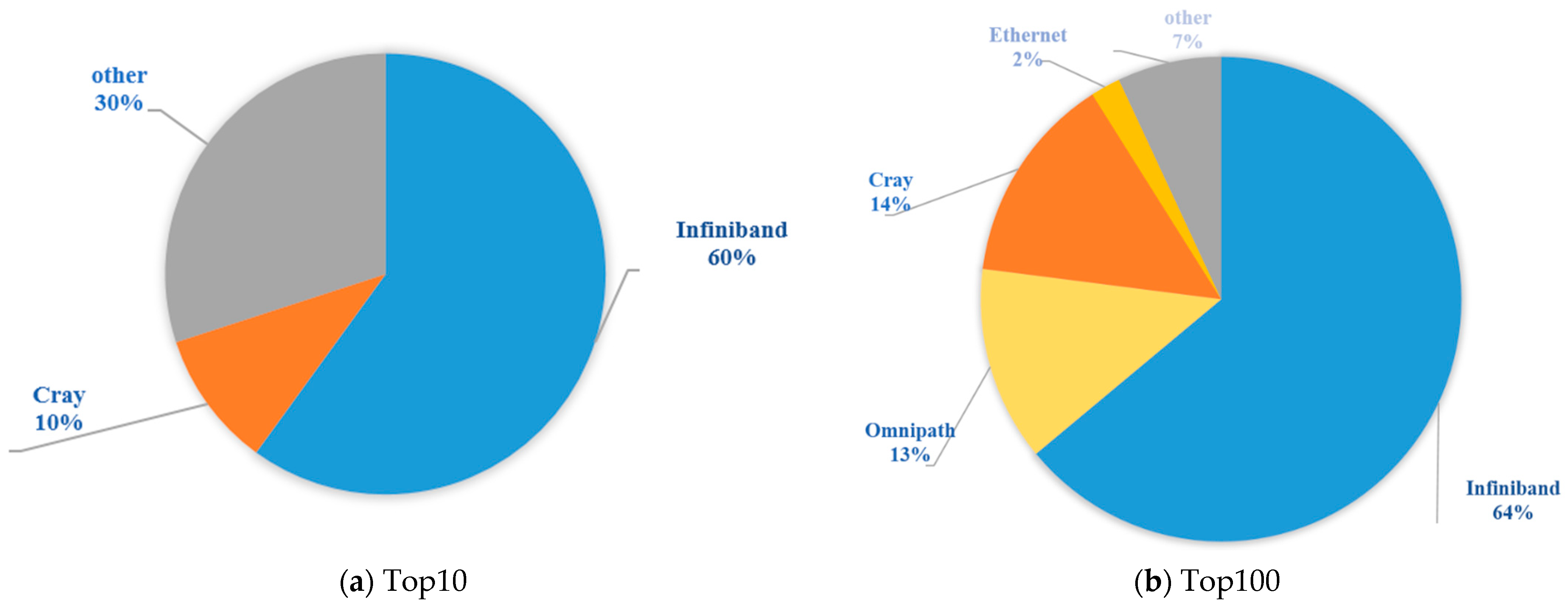
Figure 1 shows the interconnection distribution of the Top10 (
Figure 1a) and Top100 (
Figure 1b) systems in the international Top500 ranking as of November 2021.
As can be seen from
Figure 1, the high-performance interconnection network of the Top10 system includes NVIDIA’s InfiniBand interconnection (60%), Cray’s Slingshot interconnection (10%), and other custom/proprietary interconnections, including Tofu D, Sunway, and TH Express (30%). Fugaku, ranked number one, uses Tofu D, an independent, customized interconnection network; Taihu Light, ranked fifth, uses an independent customized network, Sunway; and Tianhe 2 A, ranked seventh, uses an independent customized interconnection network TH Express-2. The second-ranked Summit and the third-ranked Sierra use Mellanox EDR InfiniBand, while the sixth-ranked Selene, eighth-ranked JUWELS Booster Module, ninth-ranked HPC5, and tenth-ranked Voyager-EUS2 all use Mellanox HDR InfiniBand. The fifth-ranked Perlmutter uses Cray’s custom interconnect Slingshot-10. The proportions of interconnected networks remain the same between the Top10 and the Top100, and the distribution of ICNs in the Top100 is listed as follows: InfiniBand (64%); Cray (14%); Omni-Path (13%); other interconnected networks, including Tofu D, Sunway, TH Express, BXI, and other custom or proprietary interconnects (7%); and Ethernet above 25 Gbps (2%).
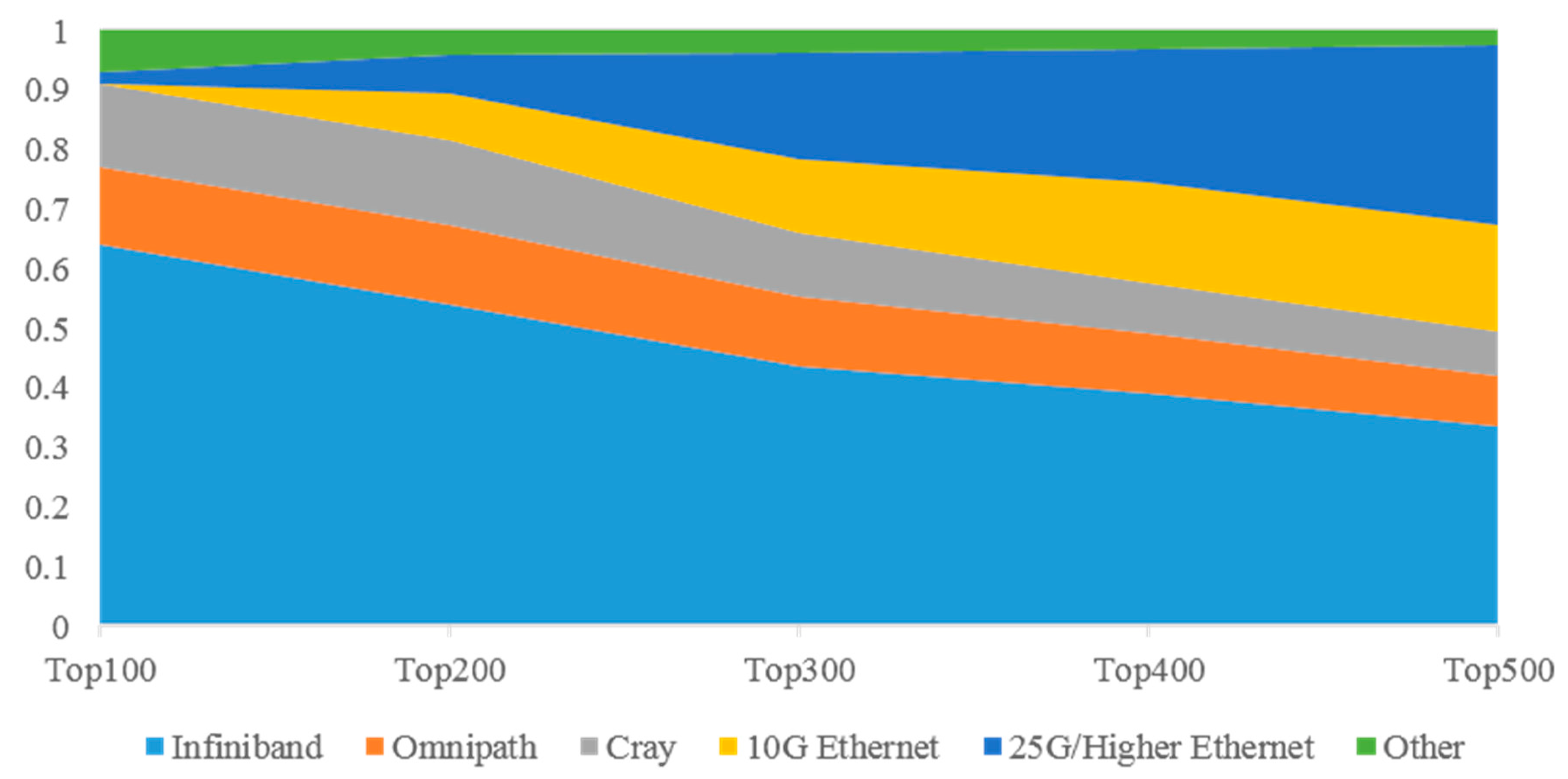
Figure 2 shows the interconnection distribution trend when the statistics of high-performance computer systems are expanded from the Top100 to the Top500. It can be seen that, with the increase in the number of statistical systems, the penetration rate of the Ethernet is rising. Many academic and industrial HPC systems cannot afford InfiniBand or are unwilling to give up Ethernet. As service providers, cloud builders, and HPC, they run Linpack on a small part of the cluster for a political or commercial reason. The relatively slow 10 Gbps Ethernet is very popular in the lower half of the Top500 list. In the list from 2021, the number of supercomputers interconnected with Ethernet has reached 240, nearly 50% of the total. The proportion of InfiniBand in the lower part of the Top500 list decreased, and its permeability decreased from 64% in the Top100 to 34% in the whole of the Top500. The reason for this phenomenon lies in the continuous improvements in Ethernet performance and the continuous reductions in the Ethernet price. The latest generation of Ethernet switches and network cards also includes important functions, such as remote direct memory access (RDMA) and intelligent network arrangement, which make Ethernet more attractive compared with traditional InfiniBand [
16].
According to the statistics of the Top500 machines, high-performance computer systems supporting HPC, artificial intelligence (AI), and Big Data have gradually become mainstream. In the future, HPC systems will not only realize high-performance computing, but they will also carry AI and Big Data analysis. In November 2021, two new systems’ “supercomputing clouds” were updated in the Top10 system, which can meet the needs of AI, HPC, and cloud computing simultaneously, and this means that HPCs are accelerating the integration with AI and cloud computing. A total of 8 of the Top10 systems use NVIDIA technology to provide acceleration, while 342 of the Top500 systems use NVIDIA technology to provide acceleration, including 70% of new systems. More and more HPC centers are using AI, which also reflects the fact that users continue to embrace the combination of NVIDIA AI, accelerated computing, and network technology to run their scientific and commercial workloads; the number of systems using InfiniBand on the list has increased by 20% since November 2020 [
16]. With the increasing demand for low latency and the acceleration of AI, HPC, and cloud computing, InfiniBand has become the preferred network of the Top500.
A summary of the main ICN properties on the Top10 list in November 2021, along with two additional, representative ICNs, is provided in
Table 1, including manufacture, interconnect family, bidirectional bandwidth, switch radix, latency, and topology. “N/A” indicates that we have not found the precise data in public reports.
In the following text, the current development statuses of ICNs are introduced, based on the typical high-performance interconnection technology adopted by the Top500.
2.1. InfiniBand ICN
The largest interconnection network active in the field of high-performance computing is the InfiniBand interconnection provided by NVIDIA. As of November 2021, 33.6% of the Top500 systems were interconnected by InfiniBand. Among Top10 systems, the second-ranked Summit and the third-ranked Sierra used Mellanox EDR InfiniBand, the sixth-ranked Selene, the eighth-ranked JUWELS Booster Module, the ninth-ranked HPC5, and the tenth-ranked Voyager-EUS2 used Mellanox HDR InfiniBand.
InfiniBand interconnect architecture [
4] is used to construct a complete system through high-speed interconnection technology for processor nodes, and the interconnection system is independent of the host operating system and processor platform. The significant feature of InfiniBand is that it supports the offloading of communication functions. It uses reliable message transmission and RDMA transmission to realize the interconnection between modules, frames, and cabinets. It can also realize the interoperability management of InfiniBand equipment from different manufacturers in different eras and provides interfaces to realize the various management functions of industry standards.
As a representative of the commercial interconnection network, InfiniBand takes the high-speed SerDes bandwidth as the intergenerational feature [
18]. After several generations of Quad Data Rate (QDR), Fourteen Data Rate (FDR), Enhanced Data Rate (EDR), High Data Rate (HDR) and Next Data Rate (NDR) development, it continues to develop in the high-end direction and supports 40 Gbps, 56 Gbps, 100 Gbps, 200 Gbps, and 400 Gbps InfiniBand networks. HDR is currently the mainstream configuration of InfiniBand interconnection network design. The HDR standard has a single link rate of 50 Gbps and a single-port bandwidth of 200 Gbps, which can meet the bandwidth requirements of current mainstream exascale high-performance computing interconnection networks. According to the Top500 in November 2021, four of the Top10 systems used InfiniBand HDR interconnections. However, in the future, HPCs may require higher standard interconnection technologies, such as upgrading the SerDes standard to the NDR, or even higher. The latest host channel adapter (HCA) ConnectX-7 and switch Quantum-2 support NDR InfiniBand 400 Gbps interconnection [
18,
19,
20].
In terms of host channel adapters, the NVIDIA ConnectX-7 provides ultra-low latency, 400 Gbps throughput, and innovative NVIDIA in-network computing engines to deliver the acceleration, scalability, and feature-rich technology needed for HPC, AI, and hyperscale cloud data centers. It supports single-port or dual-port 400 Gbps or 200 Gbps, with octal small form-factor pluggable (OSFP) connectors, and Dual-port 200 Gbps with quad small form-factor pluggable (QSFP) connectors [
19]. It supports PCIe 5.0 × 32, PCIe ×1, ×2, ×4, ×8, and ×16 configurations, and a message rate of 330–370 Mps can be achieved, which can be used for the most demanding data-center applications, providing the strongest and most flexible solution. In addition, ConnectX-7 improves Mellanox’s Multi-Host technology, supporting connections of up to four hosts [
19].
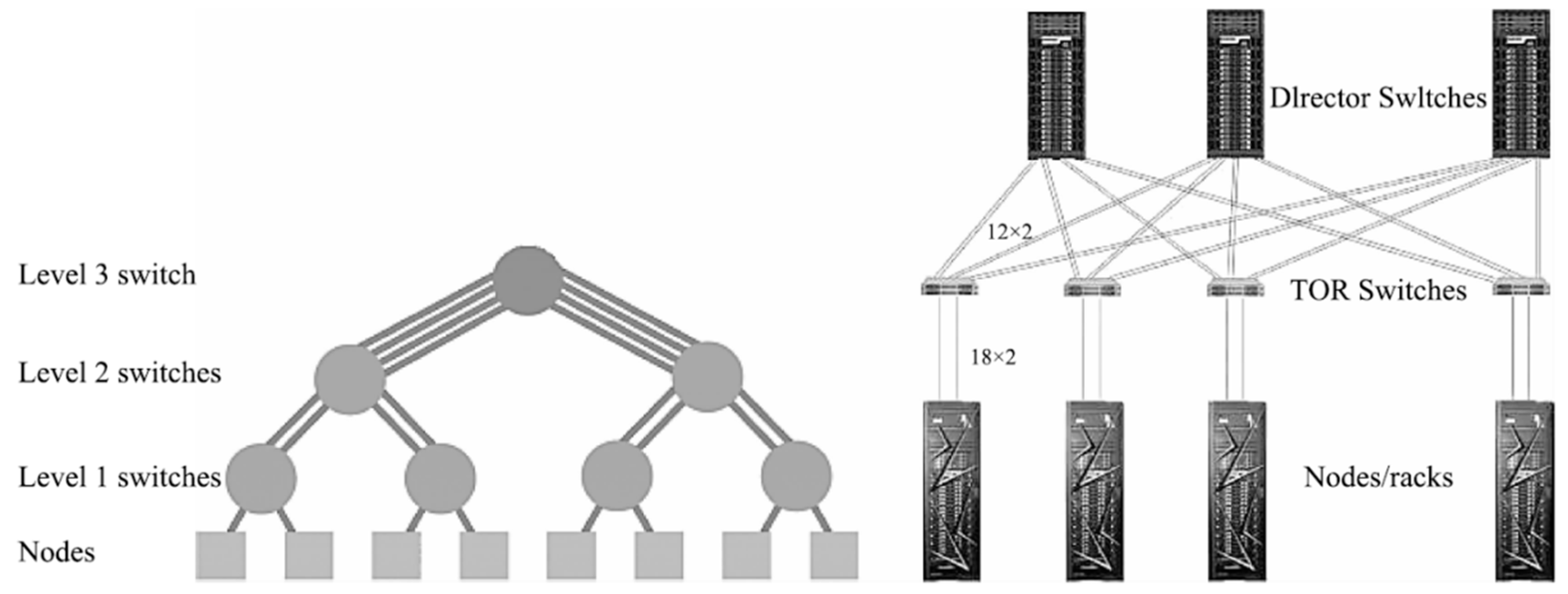
Summit (ranked 2) and Sierra (ranked 3) use EDR InfiniBand interconnects in a fat-tree network topology, as shown in
Figure 3 [
21]. Different from the traditional fat-tree topology, the Sierra interconnection network uses a 2:1 reduction ratio to reduce the fat tree, and the leaf switching node and TOR switch bandwidth have a 1:2 reduction ratio. Both the TOR (Top of Rack) switch and the leaf switching nodes use Mellanox EDR InfiniBand switching equipment with 36 ports and a single-port bandwidth of 100 Gbps for networking. EDR InfiniBand provides adaptive routing to increase data transmission speeds, which can better adapt to the needs of Big Data and AI. At the same time, it provides NVMe (non-volatile memory express) burst access acceleration, which can reduce the participation of the CPU when accessing NVMe and reduce the interruption to the CPU. The fat-tree network can isolate traffic among the computing partitions and to/from the storage subsystem, providing more predictable application performance. In addition, the high level of redundancy in this network and its reconfiguration capability ensure reliable high-performance even after network component failures [
17]. The interconnection can efficiently support the upper MPI communication software library, as well as large-scale, inter-process communication.
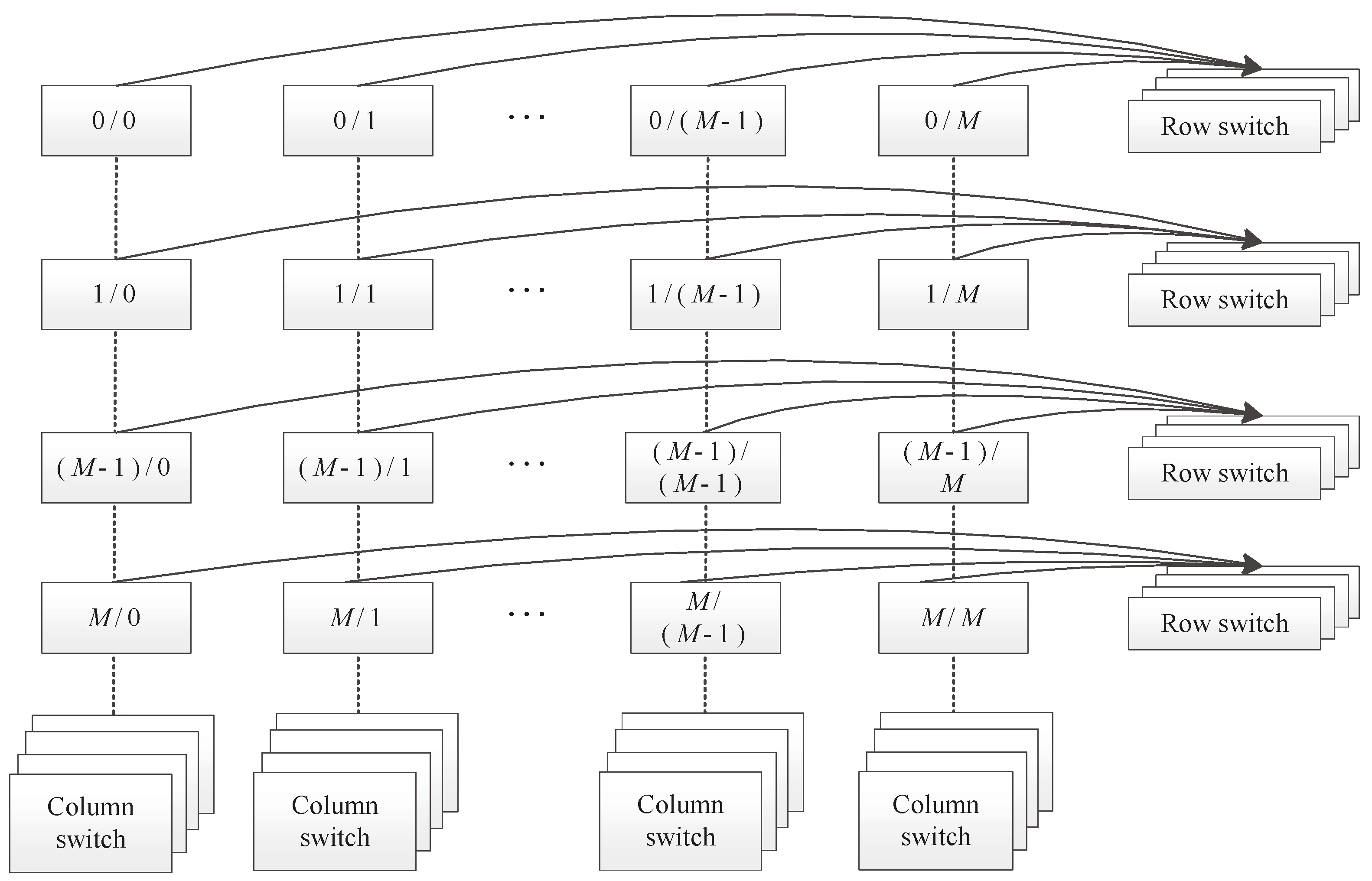
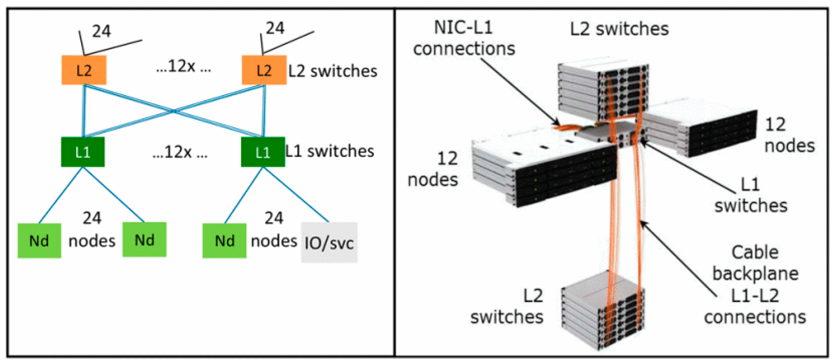
Four Top10 machines, Selene (ranked 6), JUWELS Booster Module (ranked 8) [
22], HPC5 (ranked 9), and Voyager-EUS2 (ranked 10), adopt 200 G HDR InfiniBand Interconnects, while the nodes are interconnected using the fat tree topology, combined with NVIDIA’s latest inter-node communication acceleration technology, Scalable Hierarchical Aggregation and Reduction Protocol (SHARP) 2.0, realizes the hardware acceleration of Remote Direct Memory Access (RDMA) and MPI aggregation communication processing. While ensuring sufficient network bandwidth, it reduces the communication delay between nodes and improves the efficiency of large-scale computing processing. JUWELS Booster consists of 936 compute nodes, each equipped with 4 NVIDIA A100 GPUs. The InfiniBand network of the JUWELS Booster is implemented as a dragonfly + network. A total of 48 nodes are combined in a switch group (cell) and interconnected in a full fat-tree topology, with 10 leaf switches and 10 spine switches in a two-level configuration. A total of 40 Tbps of bi-section bandwidth is available. Within a JUWELS Booster cell with 48 nodes, there are 10 level 1 switches and 10 level 2 switches. Only a small subset of the total amount of links are shown for readability. The 20th link leaving each level 2 switch should indicate the connection to the JUWELS cluster, while the other 19 outgoing level 2 links connect to other cells [
23].
The Top500 list of November 2021 shows that more and more high-performance computing centers are using AI in the Top500 systems, which also reflects the fact that users continue to embrace the combination of NVIDIA AI, accelerated computing, and network technology to run their scientific and commercial workloads. InfiniBand accounts for 34% of the Top500 interconnections, with 168 systems. The number of systems using InfiniBand has increased by 20% since November 2020, but it is not obvious that the rise of Mellanox spectrum and spectrum-2 Ethernet switches in the Top500 has increased to 148 systems. This gives NVIDIA a 63.2% share of interconnects in the Top500 [
16]. It brings together most of the InfiniBand users and many Ethernet users in Top500, which partly explains why NVIDIA spent
$6.9 billion on Mellanox. With the increasing demand of AI, HPC, and analog data for low latency and acceleration, InfiniBand has become the preferred network for the Top500.
2.2. Omni-Path ICN
The second-largest interconnection network active in the field of high-performance computing is Intel’s Omni-Path interconnect. In total, 8.4% of the systems on the Top500 list use Intel’s Omni-Path interconnect, including the 23rd-ranked SuperMUC-NG system.
Intel released the Omni-Path Architecture (OPA) specifications in 2015 [
7]. Omni-Path was a new feature added by Intel in the previous two generations of Xeon scalable processors. The Intel Omni-Path Architecture (OPA) directly descends from Cray’s Aries [
24] and Intel True Scale [
25]. True Scale leveraged the InfiniBand architecture [
26], and the Intel OPA has enhanced those capabilities by leveraging the best practices from high-performance computing interconnects. Additional innovations include an extensible, open, high-performance API framework in Performance Scaled Messaging, and more recently, the OpenFabrics Alliance’s Open Fabrics Initiative, which is amenable to creating a low-impedance interface between evolving HPC middleware and the host fabric interface (HFI) hardware/software interface [
27]. In the first-generation HFI, this resulted in low-latency, high-bandwidth implementation in which portions of the fabric protocol were executed on the processor CPU, using its multicore processing, memory, and cache resources—a so-called “onload model”. Other innovations included service-level and service-channel extensions to the virtual lane abstraction, which enabled efficient allocation of HFI and switch resources. Additionally, the link-transfer-protocol layer in the network stack enables the preempting of low-priority packets by higher-priority packets. This enables efficient bulk transfer using extended (8 K) maximum transfer unit sizes, while simultaneously reducing the latency jitter seen in tightly coupled MPI communication [
7].
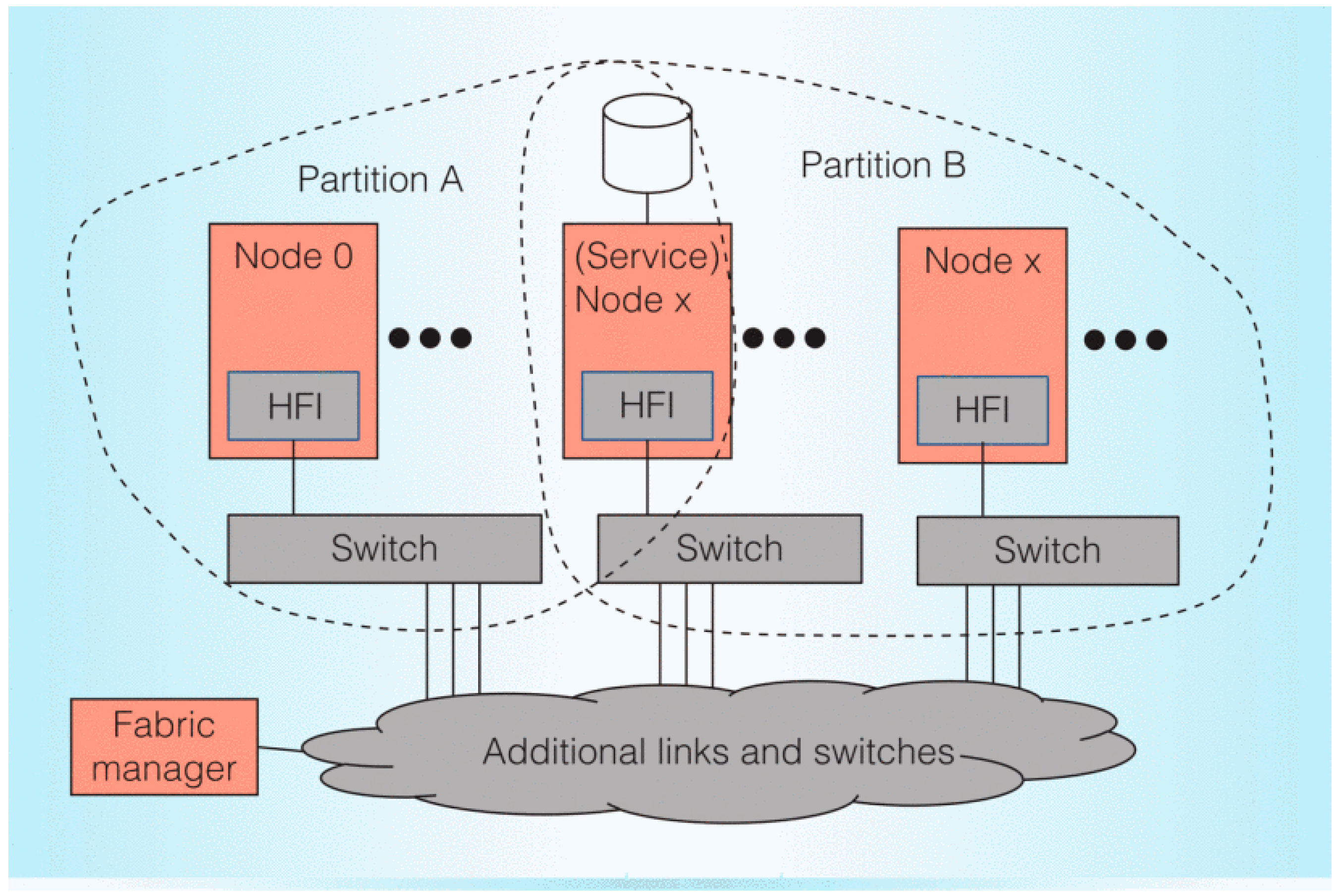
Because many network features are integrated into the CPU, Omni-Path can bring ultra-high processor interconnection performance for isomorphic supercomputing with specific Xeon processors. The main design objectives of OPA include reducing interconnection cost and power consumption, improving interconnection density, improving node bandwidth, reducing communication delay, improving MPI message rate, improving scalability, and improving system error correction capability and quality of service. As shown in
Figure 4 (reproduced with permission from [
7]), OPA components mainly include the network card, switch, and network manager. The network card is used to connect computing/service/management nodes to the network. Nodes, including service nodes, may be assigned to one or more partitions. The switch constructs several nodes into a network through the network topology. The network manager is used to centrally manage and monitor the network. The fabric is scalable, based on interconnected switch components, and is centrally managed. The OPA does not have too much offloading implementation, and a lot of work is shared by the processor kernel, which is different from the design concept of InfiniBand.
OPA’s first generation product [
28] supports a single-port 100 Gbps EDR standard, is partially compatible with InfiniBand upper layer protocol, and supports Ethernet and storage protocol expansion. The first-generation host fabric interface is code WFR (Wolf River), and the network switching chip is code PRR (Prairie River). The network interface chip WFR supports the single-port 100 Gbps EDR standard and can provide two EDR ports. Each port uses PCIe 3.0 × 16 on the host side, which can achieve a 160 Mps message rate. The network switching chip PRR provides 48 EDR ports, with a message exchange rate of about 195 M and a delay of about 100~110 ns. In order to pursue the ultimate delay performance, the chip gives up the forward error correction function and realizes error correction through retransmission at the link layer, which is acceptable in the 25 Gbps rate generation, but it is not competent for a 50 Gbps network.
Due to the need for users to purchase specific processor models, motherboard models, and dedicated switches, Omni-Path ultimately failed to be accepted by the wider market. At the end of 2019, Intel announced that it had stopped the development of the next-generation Omni-Path. Intel finally cancelled the Omni-Path product line. However, Cornelis acquired the IP and continued the development in July 2021. Omni-Path Architecture is seeking to make a comeback as an independent, high-performance interconnect solution [
29]. Cornelis is working on what it says is a significant enhancement to the OPA100 product, called Omni-Path Express (OPX). Omni-Path Express aims to win the performance and price-performance wars in the HPC interconnect marketplace [
30]. Cornelis Networks provides high-performance fabrics for HPC, High Performance Data Analytics (HPDA), and AI. Cornelis is still shipping the Omni-Path 100 Gbps (OPA100) products developed under Intel, and it is planning to launch 400 Gbps products in late 2022, with broader availability slated for the first quarter of 2023. The OPA400 product will support bifurcation to 200 Gbps. There are 800 Gbps solutions farther out on the Cornelis Omni-Path roadmap [
29].
2.3. Cray ICN
The third-largest interconnection network used in Top500 is a series of networks provided by Cray. A total of 7.4% of the systems on the Top500 list use it, including the fifth-ranked “Perlmutter” system. Cray’s interconnection products include Seastar [
31], Gemini [
32], Aries [
33,
34], and a new generation of high-performance network interconnection technology: Slingshot [
35]. In the Top100, Cray interconnection includes not only the first Slingshot machine “Perlmutter”, but also a number of machines using the previous-generation “Aries” interconnection. There were five Slingshot machines and nine Aries machines in the Top100 as of November 2021. The three next-generation exascale supercomputers (EI Capitan, Frontier, and Aurora) announced by the United States will all use Slingshot interconnect technology.
Gemini interconnect is the second-generation interconnect architecture of Cray high-performance computers. It inherited from the Seastar the highly scalable interconnect architecture of the original Jaguar system (Cray XT series) and can interconnect up to 100,000 nodes [
32]. Cray’s new Jaguar system (Cray XK6 series), Blue Waters system, and Titan have all adopted the Gemini interconnect. Cray’s third-generation interconnect architecture, Aries, is widely used in the field of high-performance computing. It adopts an integrated architecture that is tightly coupled between switching and a network interface chip. Each computing node can open 64 network interfaces, which can build a dragonfly topology with an ultra-low network diameter.
In 2019, Cray abandoned the Gemini interconnect, which integrated the architecture of tightly coupled switching and network interface chips, and the new generation of high-performance network interconnection technology, Slingshot, was launched. Slingshot is Cray’s eighth major high-performance interconnection network technology. The interconnection network technology has been in use for more than five years. Unlike previous interconnection networks, Slingshot builds high-performance interconnection protocols on standard Ethernet. Cray calls it “HPC Ethernet”. Slingshot brings the advantages of a proprietary HPC network to a highly interoperable Ethernet standard; that is, Slingshot switches first use standard Ethernet protocols to operate, but when the connected device supports advanced “HPC Ethernet” functions, it will try negotiating advanced features to support both HPC and standard Ethernet-based data centers. It has the additional advantages of standard Ethernet in order to provide support for equipment based on standard Ethernet.
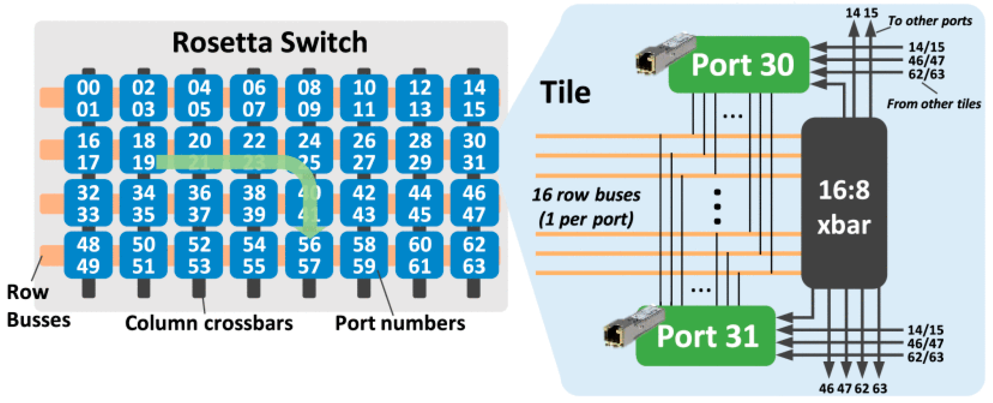
Based on the Slingshot interconnect technology, Cray implemented a switching chip, Rosetta, with a switching capacity of 12.8 Tbps in 2020. It uses the tile structure shown in
Figure 5 (reproduced with permission from [
6]), integrates 256 channels of 56 Gbps SerDes blocks using pulse-amplitude modulation (PAM-4), and can achieve 64 200 Gbps ports. The aggregate bandwidth of a single exchange node will be as high as 25.6 Tbps [
35]. Using Slingshot switches, Cray uses dragonfly topology to build large systems, but the Slingshot interconnect can support any topologies, such as dragonfly, flattened butterfly, and fat-tree. The use of the dragonfly topology is largely driven by cost so as to reduce the length of the optical cable and the cost of the system. Cray claims that up to 90% of the cables in the system are inexpensive copper cables, while optical cables account for only 10%. The Slingshot interconnect not only innovates its traditional adaptive routing algorithms, but also integrates with congestion control algorithms. The biggest advancement of Slingshot is advanced congestion control, which can quickly detect congestion. Since the bottom layer of the Slingshot interconnect is a standard Ethernet protocol, there is still a gap between the switching delay and the InfiniBand network, which is a nearly normal distribution between 300–400 ns, and the average switching delay is 350 ns, which still contains about 150 ns of error correction. However, compared with the 450 ns switching delay of a standard Ethernet network, its switching delay performance is still greatly improved [
35].
2.4. Tofu ICN
Tofu ICN is a high-performance interconnection network used by K Computer [
36] of Japan, developed by the Japanese Institute of Physics and Chemistry (RIKEN) and Fujitsu. Fugaku, ranked number one, uses Tofu D, an independent, customized interconnection network.
The Tofu D interconnect adopted by the Fugaku system, which is currently ranked first 1 in the Top500 list, is based on the Tofu network of K Computer [
10,
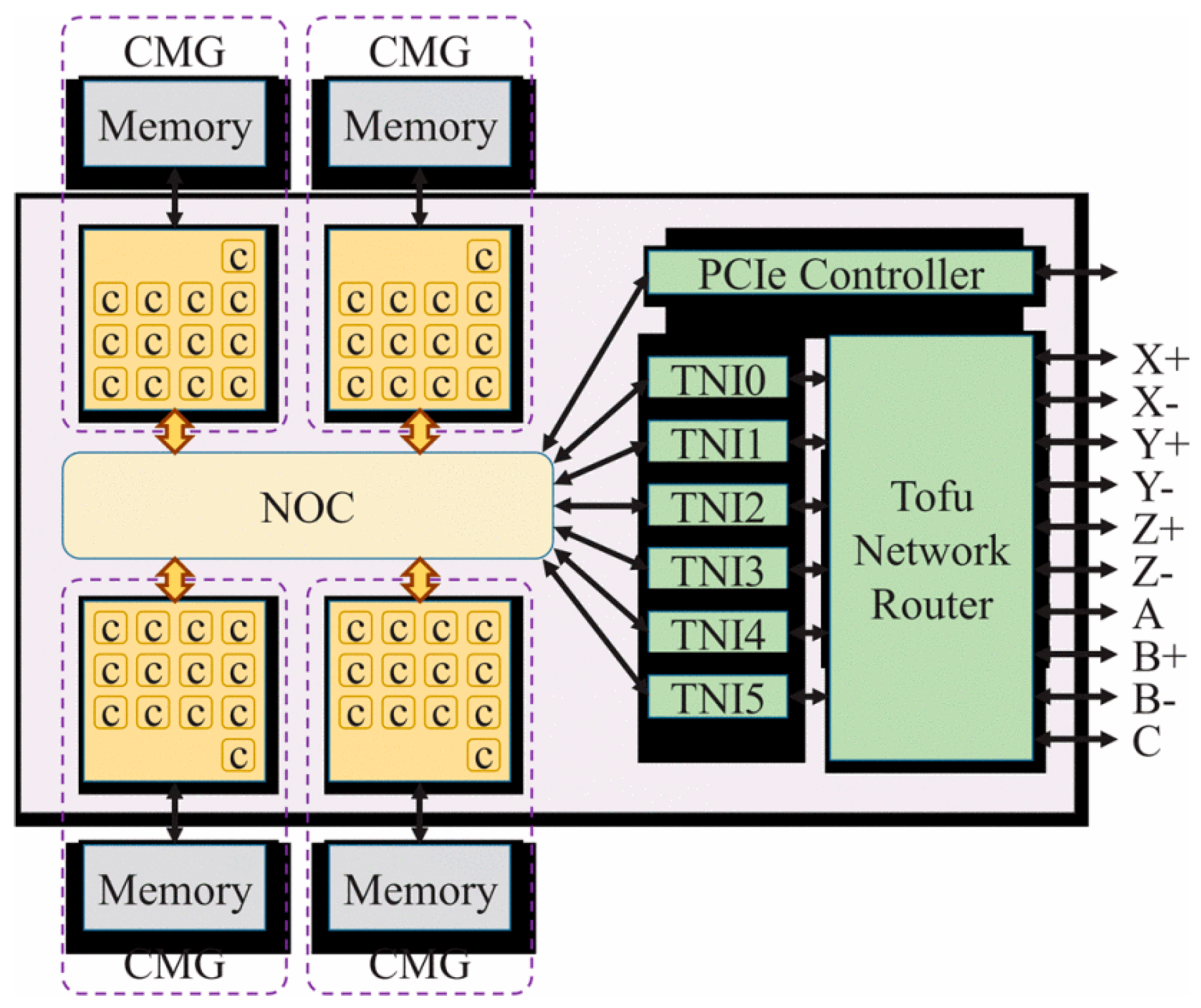
37]. The unique feature of the Tofu D interconnection system is that the multicore processor, the Tofu network routing module, and the PCIe control system form the CPU computing core A64FX through the network-on-chip (NoC) architecture.
Figure 7 (reproduced with permission from [
10]) shows a block diagram of the A64FX computer node. The A64FX contains four CMGs (core-memory groups), six TNIs (Tofu network interfaces), and one Tofu network router with 20 ports of 28 Gbps data rate, and it uses the 6D-Torus-based Tofu-D on-chip ICN. Each CMG contains 12 computing cores and 1 assistant core, and each core is marked as “c” in
Figure 6. A node address in the physical 6D network is represented by six-dimensional coordinates X, Y, Z, A, B, and C. The A and C coordinates can be 0 or 1, and the B coordinate can be 0, 1, or 2. The range of the X, Y, and Z coordinates depends on the system size. Two nodes whose coordinates are different by 1 in 1 axis and identical in the other 5 axes are “adjacent” and are connected to each other. When a certain axis is configured as a torus, the node with coordinate 0 in the axis and the node with the maximum coordinate value are connected to each other. The axes A and C are fixed to the mesh configuration, and the B-axis is fixed to the torus configuration. Each node has 10 ports for the 6D mesh/torus network. Each axis
X,
Y,
Z, and B uses two ports, and each of the axes A and C use one port [
38]. A total of 2 2 × 28.06 Gbps configuration ring network ports are provided to each of the 6 planes to provide a 54.4 Gbps link bandwidth [
10].
Compared with the previous-generation K system, the transmission rate is increased by 80%. In the virtual 3D Torus, the node contains 6 adjacent nodes, so the topology-aware algorithm can efficiently use 6 communication links at the same time. The injection bandwidth of each node reaches 326.4 Gbps, providing a one-way delay of 490 ns. The I/O of each processor uses PCIe Gen3 × 16 to connect to external devices. The A64FX’s system architecture, which integrates the network switching equipment and the CPU, can effectively shorten the transmission delay from the computing unit to the I/O, so that the I/O delay is effectively shortened, but it will also increase the complexity of the IC process. The Tofu D Interconnect also provides the Tofu Barrier’s offloading engine, which can perform aggregate communication operations without CPU intervention.
2.5. TH Express/Sunway ICN
At present, high-performance computers in China are represented by Dawning, Sunway, and Tianhe. Among them, the Dawning exascale prototype uses 200 GB 6D torus network, while Sunway and Tianhe use custom network chips [
38].
The Tianhe high-performance computer system uses the TH Express ICN developed by the National University of Defense Technology [
12,
13,
14]. TH Express is composed of two ASIC chips. One is the network interface chip (NIC), which connects various nodes in the system to the network through a host interface and provides communication services for various systems and application software. The other is a network router chip (NRC), which connects the whole system through an interconnection topology and a switching network. The Tianhe exascale prototype system is composed of 512 nodes, and the single-node network bandwidth reaches 400 Gbps. The nodes are interconnected through the multidimensional fat-tree network topology shown in
Figure 7, which can support 100,000 network nodes, and the maximum number of hops for communication between nodes does not exceed 5 [
12].
The Sunway supercomputer was developed by the National Research Center of Parallel Computer Engineering and Technology, which has been researching InfiniBand interconnection technology since 2001. It has successively introduced the SW-HCA card, the SW-Switch, complete SW-IB network management software, and InfiniBand high-level application software, and it has successively launched several commercial cluster systems [
39] based on IBA interconnection technologies. The Sunway exascale prototype is composed of multiple super nodes, and each super node contains 256 nodes. The interconnection network of the Sunway exascale prototype adopts 28 Gbps transmission technology, and the node bandwidth can reach 200 Gbps [
40]. A new generation of Sunway high-radix routers and Sunway network interface chips have been designed and released, which designed a dual-track, fat-tree topology, defined and implemented novel Sunway message primitives and message libraries, and realized a dual-track chaotic system based on packet-level granularity dynamic switching. For the order message mechanism, the communication performance is four times greater than that of the Sunway Taihu Light interconnection network. The Sunway exascale system [
38,
40,
41,
42] is based on a non-blocking, two-level fat-tree network to build a high-performance interconnection network with point-to-point, high-bandwidth communication performance.
The Dawning exascale prototype contains 512 nodes, and every 16 nodes form a super node. Using 200 Gbps Ethernet and building a network based on a 6D torus [
38], the maximum network bandwidth of a single node can reach 200 Gbps. The entire network topology is divided into three levels. The first layer is the super node layer, and the nodes inside each super node realize a full interconnection structure; the second layer realizes the interconnection structure between super nodes and multiple super nodes. The node constitutes a silicon element; the third layer is the interconnection between the silicon elements, using the 3D torus structure, and at the same time, fast optical links between the silicon elements reduce the number of communication hops, thereby improving global communication performance [
38]. The Dawning exascale interconnection architecture is expected to adopt a 500 Gbps network [
38], based on a 6D torus as the basic interconnection structure, to solve the problem of too many hops in a torus-based network, using optical fast-path technology to build a photoelectric-hybrid network architecture [
38].
2.6. Bull BXI ICN
Bull BXI (Bull eXascale Interconnect) is Bull’s first-generation exascale interconnection network architecture [
15], supporting single-port 100 Gbps. The Tera1000–2 system, ranked 42nd in the Top500 in November 2021, adopts a Bull BXI 1.2 interconnection.
BXI is different from InfiniBand’s proprietary protocol implementation and is a reliable, “order-preserving” network architecture. BXI can expand up to 64 K nodes; support multiple network topologies, such as fat-trees, torus, butterfly, etc.; support adaptive routing and flexible routing algorithm optimization; and provide deadlock-avoidance and load-balancing mechanisms.
Figure 8 (reproduced with permission from [
15]) is a schematic diagram of the network logic configuration and physical layout of the BXI architecture configured as a two-level fat-tree.
BXI is based on two ASIC chips: Lutetia, a network interface chip, and Divio, a network switch chip. Lutetia implements Portals 4 [
43,
44] communication primitives, and some functions can bypass the operating system, such as identifying logical–physical conversion; virtual–real address conversion; hardware support for Rendezvous protocol, etc.; and support the offloading function of collective communication. Divio uses 192 25 Gbps SerDes to realize 48 HDR ports, with a two-way network bandwidth of 200 Gbps, a throughput rate of 9.6 Tbps, and a delay of about 130 ns.
3. Challenges of Current High-Performance Interconnection Networks
The performance improvement of current high-performance computers mainly depends on the improvement of single-node computing performance and the increase in the number of computing nodes. As the computing power of a single node continues to increase, the communication bandwidth of the node should also increase, so as to maximize the computing performance of the node. Taking Tianhe-2 as an example, the single-node peak performance is 3 TFLOPs, while the node communication bandwidth is 112 Gbps, and the communication computation performance ratio is 0.037. In the exascale system, the peak performance of a single node can reach 10 TFLOPs [
45]. In order to maintain the communication computation ratio at 0.04, the network bandwidth has been designed to reach 400 Gbps [
46]. In the exascale high-performance computer system, the requirements for network bandwidth are higher, which presents a great challenge to the SerDes process technology at the current physical level. At the same time, as the network diameter becomes larger, the node communication delay will also increase. These are all important challenges that will be faced by supercomputers in the future [
46].
The main problems faced by interconnection networks in the exascale computing era are how to solve issues of power consumption, density, reliability, and cost, among other issues. The main challenges of interconnection networks are analyzed in the following text in terms of power consumption, reliability, and density.
3.1. Dennard’s Scaling Effect Slows Down, and Interconnection Power Consumption Is Unbearable
Although Moore’s Law held for many decades, it began to slow sometime around 2000, and by 2018, there appeared a roughly 15-fold gap between Moore’s prediction and current capability, an observation Moore made in 2003 that was inevitable [
47]. The current expectation is that the gap will continue to grow as CMOS technology approaches fundamental limits.
Accompanying Moore’s Law was a projection made by Robert Dennard called “Dennard Scaling” [
48], which states that, as transistor density increases, power consumption per transistor will drop, so the power per mm
2 of silicon will be near constant. Since the computational capability of a mm
2 of silicon increased with each new generation of technology, computers would become more energy efficient. Dennard Scaling began to slow significantly in 2007 and faded to almost nothing by 2012, as shown in
Figure 9 (reproduced with permission from [
49]). Since 2007, this scaling effect has slowed down until 2012 when the power consumption per square nanometer began to rise rapidly, resulting in an increase in energy consumption and a decrease in efficiency [
50,
51,
52]. Power consumption has become a major challenge for chip design.
With the progress of interconnection transmission technology, the system interconnection network widely adopts multichannel serial transmission technology to realize channel transmission to increase port-bandwidth [
13]. Each interconnect interface integrates one to multiple high-speed SerDes, and the transmission performance of a single SerDes has been rapidly improved from the early 1.25 Gbps to 50 Gbps. SerDes bandwidth continues to increase, enabling high-performance chips to achieve higher throughput with fewer chip pins, and it has been driving interconnection networks to higher bandwidths for many years [
52]. The performance of SerDes continues to improve, but in recent years, the SerDes power consumption per bit required to transmit has decreased slowly. According to statistics from the International Interconnection Forum, the doubling of the SerDes rate with each generation only reduces the performance per bit by 20% [
53]. Taking Tianhe supercomputers as an example, the Tianhe 1A network router chip integrates 128 channels of 10 Gbps SerDes, the total power consumption of SerDes is about 51.2 watts, and the throughput rate is 2.56 Tbps; the Tianhe 2A network router chip integrates 192 channels of 14 Gbps SerDes, and the total power consumption of SerDes is about 90 watts, while the total power consumption of the chip is about 120 watts, and the throughput rate is 5.376 Tbps [
14]. Assuming that the upper limit of the single-chip power consumption is 200 watts and the power consumption required for internal switching logic is basically maintained at about 40 watts, the number of 50 Gbps SerDes that can be integrated on a single chip is limited to about 160 channels, and the single-chip throughput rate is about 16 Tbps. If SerDes transmission efficiency cannot be improved, the number of 100 Gbps SerDes may be limited to about 80 channels, which will limit the further increase of chip throughput rate [
12].
If the SerDes performance problem is not solved properly, the system network power consumption will become unbearable. As the performance of the node continues to rise, the network bandwidth required by a single node also needs to increase accordingly. The performance problem of SerDes is not conducive to the design of high-radix networks, thereby causing a deterioration in the power consumption of the system. The current interconnection network has been moving towards high-radix networks; that is, the number of network ports integrated by a single router chip continues to increase. From the early 8 ports, it has gradually increased to 16 ports, 24 ports [
14], 36 ports [
18], 48 ports [
6,
15], and even 64 ports [
19], significantly reducing the number of routers in the network, thereby reducing the network hop count, reducing transmission delay, improving network reliability, and reducing system power consumption. According to the previous analysis, assuming a bandwidth of 800 Gbps per port, only 40 network ports can be designed under a 200-watt chip budget. It is difficult to build a high-radix network. More routers will be needed in the interconnection network, which will exacerbate power consumption issues.
3.2. SerDes Bandwidth Continues to Increase, and Interconnection Reliability Faces Greater Challenges
The HDR network can basically meet the current exascale high-performance computing interconnection requirements, but the single link rate needs to be further increased to 100 Gbps NDR in the future. Optical Interconnect Forum (OIF) has completed the formulation of 112 Gbps SerDes specifications [
54]. The high-speed interconnect has upgraded to 100 Gbps and set off a new wave of research and development. NVIDIA InfiniBand has already launched the latest host channel adapter ConnectX-7 and switch Quantum-2, which support NDR InfiniBand 400 Gbps interconnection [
18,
19,
20]. Companies, such as Inphi, InfiniBand, Jinglue Semiconductor, and Guangzi Technology, have all launched or are developing 112 Gbps SerDes to provide a physical layer foundation for a new generation of interconnection networks. Major manufacturers, such as Cisco and Huawei, will set off a wave of 800 Gbps port systems. With the increase of single-channel SerDes bandwidth, the reliability design of the interconnection network of high-performance computer systems faces greater challenges [
52].
The advent of 56 Gbps high-speed transmission makes high-speed PCB board design increasingly difficult [
55]. At present, many electrical interconnects are still used between chips. For example, routers are connected through a backplane. Even if optical interconnects are used, the switching chip and the optical module need to be connected through electrical interconnects. The higher the signal transmission rate, the higher the signal integrity requirements. The resistance–capacitance effect, signal crosstalk, reflection and many other factors, as well as the skin effect, antenna effect, and many other factors, must be considered, and the chip pin fan-out method needs to be strictly restricted [
55]. The line width, line spacing, wiring layer planning, perforating design, back-drilling, etc. of high-speed signal lines will significantly increase the difficulty of PCB board design. At the same time, due to the PCB layout and the physical structure of the system, high-speed signal lines are still required to transmit enough distance on the PCB, which will further increase the difficulty of PCB design [
52]. By using higher-quality PCB boards or increasing the number of PCB wiring layers, the corresponding difficulties can be alleviated, but it will significantly increase PCB design cost or reduce the reliability of the PCB.
The reliability of electrical signal transmission has deteriorated, and network transmission delays have increased. In large-scale network applications, the use of higher-speed electrical signal transmission is not conducive to reducing the transmission delay of the interconnection network. As the transmission rate of electrical signals continues to increase, the crosstalk effect, electromagnetic noise, signal reflection, and other phenomena of the SerDes signal on the PCB will reduce the reliability of signal line transmission [
52]. Below the 14 Gbps link rate, it is usually assumed that the signal transmission error rate can reach 10
−12, and above the 25 Gbps link rate, it is usually assumed that the signal transmission error rate can reach 10
−9, and the reliability is reduced by 3 orders of magnitude [
55]. In order to achieve high-reliability data transmission on low-reliability links, coding techniques with stronger error-correction capabilities at the link layer are required, such as forward error correction (FEC). These coding techniques will significantly increase network transmission delay while improving reliability. According to experience, under the condition of not using FEC encoding, the single-chip delay is 100 ns; using FEC encoding, the delay increases to 500 ns, and the network transmission delay deteriorates significantly.
If we continue to adopt the existing scheme, the crosstalk effect, reflection effect, and signal attenuation caused by the 100 Gbps signal passing through a long transmission path will become the key factors affecting reliability. In comparison, optical signals are multiplexed with different wavebands for light-wave transmission, and there is no signal distortion or clock distortion, and data crosstalk is significantly reduced [
56,
57,
58].
3.3. With the Widening Gap between Processor Performance and SerDes-Port Rate, the Difficulty of Engineering Density Implementation of Interconnects Is Growing
Density is an important factor affecting system reliability, performance, and scalability in HPC computers [
48].
The first factor is the pin density of the chip’s effective high-speed signals. With the continuous improvement of chip design technology, the size of transistors continues to decrease, and more design resources can be integrated in a single chip. On the other hand, the number of pins on the chip has increased very slowly. The
ITRS (International Technology Roadmap for Semiconductors) [
59] predicted that the maximum number of chip I/Os in 2007, 2015, and 2022 would be 2200, 2800, and 3420, respectively. For a long period of time, the slow increase in the number of I/Os will be difficult to meet the I/O demand. Increasing the bandwidth of a single chip pin can alleviate the dilemma of slow growth in the number of pins to a certain extent. For example, the memory access interface of the processor has been gradually upgraded from DDR2 to DDR4, and the memory access bandwidth of the processor can still be continuously improved under the limited pin constraints. However, considering high-speed pins above 10 Gbps, increasing the pin rate may result in a decrease in the effective pin density, thereby affecting the increase in pin bandwidth. This occurs mainly because higher speed pins have higher power consumption and may require more power pins; in addition, higher speed pins need to add more ground (GND) pins due to signal integrity constraints, to achieve isolation between high-speed signals. According to engineering experience, the number of pins developed in recent generations of switching chips has only increased from more than 2500 to more than 2800, an increase of only 8.6%. Although continuous improvements in integrated circuit technology and packaging have slightly increased the number of I/Os, it has been found that the density of high-speed signals has decreased, and the number of high-speed signals has decreased by 25%. A higher single-channel transmission rate means higher power consumption and requires more power pins and GND pins. As the interconnection transmission rate increases, the chip’s high-speed pin density decreases instead. This problem will cause a decline in the number of network-switching chip ports in the future, a slow increase in chip switching throughput, an increase in the hop count of network interconnections, and a limited scalability of network scale.
The second factor is the density of PCB boards. At present, there are two main factors that limit the increase of PCB board density. First, with the increase of SerDes bandwidth in the chip, in order to ensure the integrity of the SerDes signal, it is necessary to set aside the SerDes signal in the chip-packaging design and PCB design [
12]. Larger line spacing results in greater fan-out area requirements for chip signals, and it is difficult to increase the PCB design density. second, optoelectronic hybrid transmission technology is widely used to build large-scale systems [
56,
57]. The PCB board needs to integrate the optical module. Due to the characteristic requirements of the optical module, the optical module is usually installed on the edge of the PCB or on the panel. Constrained by the size of the PCB board, the number of optical modules that can be integrated on a single PCB board is very limited, usually no more than 24 in a row, which also limits the increase in PCB density. Even if more expensive on-board optical modules are used, the density could only be increased by about three-fold, and it will still be difficult to meet the design density requirements of HPC in the future.
The above-mentioned chip pin-density problem and PCB board-density problem make it difficult to effectively improve the network engineering density. In the field of high-performance computers, a considerable number of switches and optical-fiber copper cables have become the main factors affecting network engineering. According to Moore’s Law, the performance of high-performance processors doubles every 18 months, which was claimed in 1975 [
60] although it began to slow sometime around 2000, and by 2018, there appeared a roughly 15-fold gap between Moore’s prediction and then-current capability; Moore observed in 2003 that this was inevitable. The current expectation is that the gap will continue to grow as CMOS technology approaches fundamental limits [
47]. Meanwhile, the SerDes-port rate doubles every 3 to 4 years with each change [
56]; therefore, the gap between processor performance and port rate is widening gradually. In high-performance computers, in order to maintain a globally balanced performance communication ratio, the number of switches is often increased in exchange for an increase in aggregate bandwidth. For example, the Tianhe 2A supercomputer requires 125 computer cabinets and 13 communication cabinets; the Sunway supercomputer requires 48 cabinets and 8 communication cabinets.
With improvements in computing performance, the ratio of communication cabinets to computer cabinets has become the bottleneck of network engineering [
21]. If the existing structure continues to be used, the number of high-performance system communication cabinets may exceed the number of computer cabinets, and the engineering density of interconnection networks will face major challenges.
4. Trend of High-Performance Interconnection Networks
A high-performance interconnection network is the essential facility of HPCs. At present, mainstream, high-performance interconnection is developing rapidly, showing four trends. First, high-performance interconnection takes the lead in aiming at 100 Gbps line speed to increase interconnection communication bandwidth. Second, in order to reduce transmission delay, interconnection and computing continue to merge and deepen cooperation. Third, there is the adoption of a multiprotocol network convergence architecture to reduce costs. Fourth, chiplet-based optoelectronic common-mode integrated packaging is improving system density.
In the future, Moore’s Law is facing multiple pressures from physical limits and economic constraints [
47]. The development of high-performance computers represents the forefront of the development of electronic information technology. It is recommended that optical computers add silicon-optical integration for high-performance computing, based on carbon nanotubes to replace silicon-based semiconductors [
57], and the integration of computing and networks to strengthen the disruptive breakthroughs in basic cutting-edge technologies. The high-performance interconnection network is planned to extend in the three main directions of “More Moore” [
47], “More than Moore” [
47], and “Beyond CMOS” [
55], from the aspects of disruptive new technologies, such as system integration, system packaging, new materials, new devices, etc [
53]. We must explore technological breakthroughs, solve the technical bottlenecks of ultra-high speed, ultra-low latency, high density, low cost, and high reliability in the ultra-large-scale network in the future, and realize a new type of intelligent and integrated high-performance interconnection network.
4.1. System Integration Based on the Integration of Computing and Interconnect and Convergence of Multiple Networks
“More Moore” [
47] involves continuing the essence of Moore’s Law, with the goal of reducing the size of digital integrated circuits, while optimizing devices with both performance and power consumption.
With the advancement of chip-design technology, the performance of computing nodes including single processors/accelerators is rapidly improving, and the transmission delay of interconnect networks is required to be reduced accordingly. Under the framework of the existing technology, the processor and the computing node are connected to the system interconnection network through the network interface chip. The computing node and the network interface realize the I/O structure connection through the PCIe interconnection. In an end-to-end network communication process, data needs to pass through the PCIe interface twice, and the PCIe communication delay occupies a large proportion of the total delay (consuming about 66% of the total end-to-end delay). In view of PCIe’s I/O interconnection and loosely coupled storage architecture, it is difficult to further reduce latency and meet even response requirements. Therefore, if the consistency maintenance of the shared data between the computing node and the network interface can be realized, the access of the network interface is directly supported in the consistency domain of the processor without the I/O space mapping of PCIe, which can significantly reduce network delay, and improve network performance. At the same time, with the rise of 5G, cloud computing, AI, and other technologies, as well as the continuous improvement of network transmission rates, the amount of data sent and received by the processor and the amount of calculation and storage data have increased exponentially. Only the processing of network protocols has overwhelmed the servers’ CPUs. For example, to process 10 Gbps network packets in real time, about 4 Xeon CPU cores are required. Network packet processing alone can take up half of the computing power of an 8-core, high-end CPU. If you consider 40 Gbps in 100 Gbps high-speed networks, the performance overhead is even more unbearable.
By integrating a certain number of processor computing cores in the traditional network interface, the computing power is extended to the edge of the network, and some tasks originally processed by the server’s CPU are offloaded to the network interface, realizing the integration of computing and communication [
61,
62,
63], which is also called SmartNIC (smart network interface card) [
64,
65] technology. SmartNICs offload from server CPUs an expanding array of jobs required to manage modern distributed applications. It can enable the server’s CPU to focus on complex calculations and critical processing tasks. In the network interface chip, functions such as storage, encryption and decryption, aggregate communication, deep packet inspection, and complex routing can be completed, which will greatly reduce the computational burden of the server’s CPU, thereby improving the performance of the entire network. The PCIe is replaced by a consistent inter-chip interconnect interface to reduce data transmission delay. At the same time, a certain number of streamlined processor cores are integrated in the network interface to realize the offloading of computing node tasks to the network interface and realize the deep integration of networking and computing. An important means to achieving low latency, low power consumption, and high-density interconnection is also an important development trend in next-generation interconnection networks.
In addition, with the convergence trend of HPC, Big Data, and AI computing, multinetwork convergence is an important trend in the development of interconnection networks in the future, which is mainly reflected in two aspects. First, the Ethernet protocol widely used in data centers by supporting RoCE (RDMA over Converged Ethernet), iWARP, and other new technologies, it is continuously integrated into HPC high-speed networks, which greatly reduces the transmission delay of remote memory access communication, and it provides better support for high-performance computing and AI computing applications; the second is the adoption of InfiniBand EoIB protocol to merge with Ethernet [
18,
19,
20].
NVIDIA has been committed to the integration of the InfiniBand high-performance network and the Ethernet network, launching a variety of multinetwork integration chip products, and its latest network provides data-center application support, and it provides a block-level encryption function. Data must be encrypted during transmission and decrypted when stored or retrieved by hardware. It supports protection among users sharing the same resources, reduces latency, and reduces CPU load. It complies with Federal Information Processing Standards, which reduces the system’s requirements for self-encrypting disks; through communication accelerators, scalable hierarchical aggregation and reduction technology, it can meet the network bandwidth and delay requirements from high-performance computing to machine learning, and even the most demanding applications. InfiniBand’s Harrier network is based on HPC interconnection, which integrates PCIe networks, 100 G Ethernet, and monitoring and management networks; PLX originally focused on PCIe Switch, but it now gradually develops towards PCIe networking based on multiple PCIes [
66,
67]. Cray’s new generation of Slingshot interconnection adopts the “HPC Ethernet” architecture to achieve the convergence of the high-performance interconnect network and Ethernet. Expanding the traditional high-performance interconnection technology to support the data center network protocol stack has become an important development trend in the current, international, high-speed interconnection field.
4.2. D-System Integrated Packaging Based on Optoelectronic Fusion and Chiplets
“More than Moore” [
47] involves the improvement of chip performance which no longer relies on purely stacked transistors, but more on circuit design and system algorithm optimization; at the same time, with the help of advanced packaging technology to achieve heterogeneous integration, that is, relying on digital chip modules realized by advanced technology integrated to improve chip performance.
With the expansion of system scale and the improvement of communication bandwidth, optical interconnection has increasingly become an important implementation technology that cannot be bypassed in the construction of large-scale interconnection networks, and the trend of optical interconnection technology to further penetrate into board-level and chip-package-level designs is also increasing [
61,
62]. High-density optoelectronic integration technology is currently the most important enabling technology for improving chip-integration density and system-interconnection density, and it is also a currently an area of great international research interest [
68]. Chiplet-based 2.5D integrated packaging is also the trend of future chip packaging. Samples of EPI’s first CPU prototype EPAC 1.0 test chip based on the 22 nm process using the RISC-V architecture were launched in 2021 [
69]. In the EPI (European Processor Initiative) project plan, each processor will contain four VPUs (vector processors) as well as EXTOLL ultra-high-speed network on chips and SerDes interconnect technology. The chips are expected to be packaged as chiplets. The RHEA SoC using ARM architecture will contain 72 Arm Neoverse Zeus cores, a mesh grid layout, 2.5D packaging, integrated HBM and network interconnect modules, and will be manufactured using TSMC’s 6 nm process [
53]. This includes the involvement of many chip giants in the silicon photonics industry, and several silicon-based optoelectronic hybrid-chip-design start-ups, such as Ayar Labs in the United States, Rockley in the United Kingdom, RANOVUS in Canada, Sicoya in Germany, and Leti in France, have sprung up. Silicon-based optoelectronic integration is used in applications. The general promotion will usher in an explosion.
4.3. Beyond CMOS: Exploration of New Devices and New Materials
“Beyond CMOS” [
53] involves exploring new principles, new materials, and new structures of devices and circuits, developing towards nano, sub-nano, and multifunctional devices, and inventing and simplifying new information-processing technologies so as to replace CMOS devices with fabric limits.
The development of high-performance computers represents the development frontier of electronic information technology. We suggest strengthening the subversive breakthrough of basic frontier technology in optical computers for high-performance computing in the future and the substitution of silicon-based semiconductors based on carbon nanotubes.
New devices based on the principles of optical computing and superconducting computing are an important direction for the reform of Dawning supercomputer processor devices in the future [
53]. Compared with electrical signals, light has strong anti-interference and parallelism. Digital computing systems and analog computing systems built based on optical principles have great computing potential in several fields. The constructed high-speed and low-power computing system has great advantages in computing power and power consumption; for example, the monolithic optical matrix computing chip can complete a neuron operation of 2 petaops per second, and the power consumption is only tens of watts [
58]. The photonic devices that can be integrated on a single chip show exponential growth, which meets the needs of building optical computing systems in the future at the device level. In traditional electronic computers, the power consumption of the processor core is the main factor limiting the improvement of processor main frequency [
61]. At present, the operating frequency of a processor used in high-performance computers is generally lower than 5 GHz, which limits the computing power of the whole computing system; the superconducting calculator device uses the non-resistance characteristic of the material when it is close to absolute zero to eliminate the loss and heat generated when a current passes through it. The power consumption problem is no longer the limiting factor for the improvement of the processor core dominant frequency. Therefore, the processing core dominant frequency constructed based on the superconducting device can reach 50 GHz or even higher. As a progressive technology, the application of superconducting devices solves the two problems of power consumption and heat dissipation at the same time and will improve the energy efficiency ratio of high-performance computers by 100 times in the future [
53].
In addition, with the improvement of the silicon-based CMOS process, the channel will be shorter and shorter, and the short channel effect will be more and more prominent, which will make the transistor current leakage larger and larger. In addition, the manufacturing process difference will have an increasing impact on the device, and the physical bottleneck faced by Moore’s Law is already becoming more and more serious. Among the few possible alternative materials, carbon-based nano materials (especially carbon nanotubes and graphene) are recognized as the most promising materials to replace silicon because they are faster and consume less power than silicon-based devices and have a high intrinsic mobility of electrons and holes at room temperature, which exceeds the best semiconducting materials [
55]. We should explore carbon nanotubes as a new material for semiconductor manufacturing instead of silicon-based semiconductors. Manufacturing carbon nanotube field effect transistors (CNFET) has become the main goal of the next generation of high-performance computers. In response to the arrival of the post-Moore era, the Defense Advanced Research Projects Agency (DARPA) [
70,
71] launched the Electronics Resurgence Initiative (ERI) [
72]. Among its components, the DSOC project is the most highly funded project among the six projects [
73]. The goal is to find new material forms, such as carbon nanotubes, and use monolithic 3D integration technology to realize the ability to provide 7 nm-chip energy efficiency using a 90 nm process, and the performance per power consumption will be improved by more than 50-fold. The research shows that CNFET has about 10 times the energy efficiency and faster running speed of silicon. Functionally, CNFET can be used to replace traditional, silicon-based transistors and build complex logic circuits. CNFET replaces the Si-based channel of traditional MOSFET transistors with a row of carbon nanotubes. Compared with silicon-based CMOS technology, CNFET has the advantages of higher conduction efficiency and faster speed, which improve the energy efficiency by more than 10 times. The construction of a carbon nano-transistor can be completed below 400 °C without damaging the circuits of other layers and can achieve better channel control [
68]. Therefore, the chip research on carbon-based nano materials has attracted much attention in recent years, especially in the United States, which will provide a new way forward when Moore’s Law comes to an end.
5. Conclusions
Supercomputers have entered the era of exascale computing, and exascale computing systems continue the technical roadmap of improving processor performance and increasing the number of processors. The computing power of a single processor exceeds 10 TFLOPs, and the difficulty and cost of providing balanced communication capabilities are far greater than the increase in computing power. The number of processors exceeds 100,000, the number of communication lines exceeds millions, and integrated circuits are gradually entering the post-Moore era, which has brought huge challenges to high-performance interconnection networks, including those involving power consumption, density, scalability, reliability, and the cost of the system of the interconnection network. The trends of high-performance interconnection network technology include, first, 100 Gbps line-speed-based high-speed interconnections improves interconnection communication bandwidth; second, the integration of interconnections and computing reduces transmission delays; third, multiprotocol network convergence architecture reduces cost; fourth, chiplet-based optoelectronic integrated packaging improves system density. In the exascale computing era, the design of high-performance computer interconnection networks needs to adopt new packaging-process technology, new design technology, new materials, new devices, and other disruptive, new technologies to achieve technological breakthroughs.


